EP2666548A2 - Transducteur ultrasonique, sonde à ultrasons et appareil de diagnostic à ultrasons - Google Patents
Transducteur ultrasonique, sonde à ultrasons et appareil de diagnostic à ultrasons Download PDFInfo
- Publication number
- EP2666548A2 EP2666548A2 EP13168517.4A EP13168517A EP2666548A2 EP 2666548 A2 EP2666548 A2 EP 2666548A2 EP 13168517 A EP13168517 A EP 13168517A EP 2666548 A2 EP2666548 A2 EP 2666548A2
- Authority
- EP
- European Patent Office
- Prior art keywords
- ultrasonic
- opening
- substrate
- supporting film
- ultrasonic transducer
- Prior art date
- Legal status (The legal status is an assumption and is not a legal conclusion. Google has not performed a legal analysis and makes no representation as to the accuracy of the status listed.)
- Withdrawn
Links
Images




Classifications
-
- H—ELECTRICITY
- H04—ELECTRIC COMMUNICATION TECHNIQUE
- H04R—LOUDSPEAKERS, MICROPHONES, GRAMOPHONE PICK-UPS OR LIKE ACOUSTIC ELECTROMECHANICAL TRANSDUCERS; ELECTRIC HEARING AIDS; PUBLIC ADDRESS SYSTEMS
- H04R17/00—Piezoelectric transducers; Electrostrictive transducers
-
- B—PERFORMING OPERATIONS; TRANSPORTING
- B06—GENERATING OR TRANSMITTING MECHANICAL VIBRATIONS IN GENERAL
- B06B—METHODS OR APPARATUS FOR GENERATING OR TRANSMITTING MECHANICAL VIBRATIONS OF INFRASONIC, SONIC, OR ULTRASONIC FREQUENCY, e.g. FOR PERFORMING MECHANICAL WORK IN GENERAL
- B06B1/00—Methods or apparatus for generating mechanical vibrations of infrasonic, sonic, or ultrasonic frequency
- B06B1/02—Methods or apparatus for generating mechanical vibrations of infrasonic, sonic, or ultrasonic frequency making use of electrical energy
- B06B1/06—Methods or apparatus for generating mechanical vibrations of infrasonic, sonic, or ultrasonic frequency making use of electrical energy operating with piezoelectric effect or with electrostriction
- B06B1/0644—Methods or apparatus for generating mechanical vibrations of infrasonic, sonic, or ultrasonic frequency making use of electrical energy operating with piezoelectric effect or with electrostriction using a single piezoelectric element
-
- A—HUMAN NECESSITIES
- A61—MEDICAL OR VETERINARY SCIENCE; HYGIENE
- A61B—DIAGNOSIS; SURGERY; IDENTIFICATION
- A61B8/00—Diagnosis using ultrasonic, sonic or infrasonic waves
- A61B8/44—Constructional features of the ultrasonic, sonic or infrasonic diagnostic device
- A61B8/4444—Constructional features of the ultrasonic, sonic or infrasonic diagnostic device related to the probe
-
- B—PERFORMING OPERATIONS; TRANSPORTING
- B06—GENERATING OR TRANSMITTING MECHANICAL VIBRATIONS IN GENERAL
- B06B—METHODS OR APPARATUS FOR GENERATING OR TRANSMITTING MECHANICAL VIBRATIONS OF INFRASONIC, SONIC, OR ULTRASONIC FREQUENCY, e.g. FOR PERFORMING MECHANICAL WORK IN GENERAL
- B06B1/00—Methods or apparatus for generating mechanical vibrations of infrasonic, sonic, or ultrasonic frequency
- B06B1/02—Methods or apparatus for generating mechanical vibrations of infrasonic, sonic, or ultrasonic frequency making use of electrical energy
- B06B1/06—Methods or apparatus for generating mechanical vibrations of infrasonic, sonic, or ultrasonic frequency making use of electrical energy operating with piezoelectric effect or with electrostriction
- B06B1/0607—Methods or apparatus for generating mechanical vibrations of infrasonic, sonic, or ultrasonic frequency making use of electrical energy operating with piezoelectric effect or with electrostriction using multiple elements
- B06B1/0622—Methods or apparatus for generating mechanical vibrations of infrasonic, sonic, or ultrasonic frequency making use of electrical energy operating with piezoelectric effect or with electrostriction using multiple elements on one surface
-
- G—PHYSICS
- G01—MEASURING; TESTING
- G01N—INVESTIGATING OR ANALYSING MATERIALS BY DETERMINING THEIR CHEMICAL OR PHYSICAL PROPERTIES
- G01N29/00—Investigating or analysing materials by the use of ultrasonic, sonic or infrasonic waves; Visualisation of the interior of objects by transmitting ultrasonic or sonic waves through the object
- G01N29/22—Details, e.g. general constructional or apparatus details
- G01N29/24—Probes
-
- G—PHYSICS
- G01—MEASURING; TESTING
- G01S—RADIO DIRECTION-FINDING; RADIO NAVIGATION; DETERMINING DISTANCE OR VELOCITY BY USE OF RADIO WAVES; LOCATING OR PRESENCE-DETECTING BY USE OF THE REFLECTION OR RERADIATION OF RADIO WAVES; ANALOGOUS ARRANGEMENTS USING OTHER WAVES
- G01S15/00—Systems using the reflection or reradiation of acoustic waves, e.g. sonar systems
- G01S15/02—Systems using the reflection or reradiation of acoustic waves, e.g. sonar systems using reflection of acoustic waves
-
- G—PHYSICS
- G10—MUSICAL INSTRUMENTS; ACOUSTICS
- G10K—SOUND-PRODUCING DEVICES; METHODS OR DEVICES FOR PROTECTING AGAINST, OR FOR DAMPING, NOISE OR OTHER ACOUSTIC WAVES IN GENERAL; ACOUSTICS NOT OTHERWISE PROVIDED FOR
- G10K13/00—Cones, diaphragms, or the like, for emitting or receiving sound in general
-
- G—PHYSICS
- G10—MUSICAL INSTRUMENTS; ACOUSTICS
- G10K—SOUND-PRODUCING DEVICES; METHODS OR DEVICES FOR PROTECTING AGAINST, OR FOR DAMPING, NOISE OR OTHER ACOUSTIC WAVES IN GENERAL; ACOUSTICS NOT OTHERWISE PROVIDED FOR
- G10K9/00—Devices in which sound is produced by vibrating a diaphragm or analogous element, e.g. fog horns, vehicle hooters or buzzers
- G10K9/12—Devices in which sound is produced by vibrating a diaphragm or analogous element, e.g. fog horns, vehicle hooters or buzzers electrically operated
- G10K9/122—Devices in which sound is produced by vibrating a diaphragm or analogous element, e.g. fog horns, vehicle hooters or buzzers electrically operated using piezoelectric driving means
-
- H—ELECTRICITY
- H10—SEMICONDUCTOR DEVICES; ELECTRIC SOLID-STATE DEVICES NOT OTHERWISE PROVIDED FOR
- H10N—ELECTRIC SOLID-STATE DEVICES NOT OTHERWISE PROVIDED FOR
- H10N30/00—Piezoelectric or electrostrictive devices
- H10N30/101—Piezoelectric or electrostrictive devices with electrical and mechanical input and output, e.g. having combined actuator and sensor parts
-
- H—ELECTRICITY
- H10—SEMICONDUCTOR DEVICES; ELECTRIC SOLID-STATE DEVICES NOT OTHERWISE PROVIDED FOR
- H10N—ELECTRIC SOLID-STATE DEVICES NOT OTHERWISE PROVIDED FOR
- H10N30/00—Piezoelectric or electrostrictive devices
- H10N30/80—Constructional details
- H10N30/88—Mounts; Supports; Enclosures; Casings
Definitions
- the present invention relates to an ultrasonic transducer, an ultrasonic probe, and an ultrasonic examination device.
- This ultrasonic transducer in which a plurality of ultrasonic elements are arranged in a matrix pattern has been known.
- This ultrasonic transducer includes a substrate that has a plurality of openings, a supporting film that is provided on the substrate so as to cover each of the openings, and a piezoelectric element that is provided on a part of the supporting film corresponding to each of the openings.
- a diaphragm is constructed by the part of the supporting film corresponding to the opening which is a part coinciding with the opening of the supporting film in a planar view.
- the ultrasonic element is constructed by the diaphragm and the piezoelectric element provided on the diaphragm.
- the thickness of the supporting film of the ultrasonic transducer that is, the thickness of the part of the supporting film corresponding to the opening which coincides with the opening of the supporting film in a planar view is set to be uniform (for example, see Patent Document 1).
- the diaphragm is greatly deflected when ultrasonic waves are transmitted, and the diaphragm is slightly deflected when ultrasonic waves are received.
- the well-known ultrasonic transducer has a problem that the diaphragm is greatly deflected especially when ultrasonic waves are transmitted, which causes the stress to concentrate in the vicinity of an outer edge portion of the diaphragm and causes damage such as cracking or chipping.
- the diaphragm will become hard to deflect.
- the deflection amount of the diaphragm will become smaller, which makes the stress generated in the piezoelectric element very small. Consequently, the level of a reception signal output from the piezoelectric element will be deteriorated. In other words, the characteristics of transmission and reception of ultrasonic waves, in particular, the sensitivity in reception will be deteriorated.
- Patent Document 1 Japanese Laid-open Patent Publication No. 2000-23296 is an example of the related art.
- the object underlying the invention is to provide an ultrasonic transducer, an ultrasonic probe, and an ultrasonic examination device which have good characteristics of transmission and reception of ultrasonic waves, and can prevent the part of the supporting film corresponding to the opening from being damaged.
- an ultrasonic transducer includes the features of claim 1.
- an ultrasonic transducer includes the features of claim 3.
- the invention also provides an ultrasonic probe, and an ultrasonic examination device as recited in claim 8 and 9, respectively.
- Fig. 1 is a perspective view showing an embodiment of an ultrasonic probe according to the invention
- Fig. 2 is a plan view showing an ultrasonic transducer of the ultrasonic probe shown in Fig. 1 ;
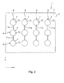
- Fig. 3 is a plan view enlarging a part of the ultrasonic transducer shown in Fig. 2 ;
- Fig. 4 is a sectional view along line A-A of Fig. 3 ;
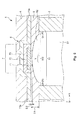
- Fig. 5 is a sectional view enlarging a part of the ultrasonic transducer shown in Fig. 4 ;
- Figs. 6A-6D are sectional views explaining a method for manufacturing the ultrasonic transducer of the ultrasonic probe shown in Fig. 1 ;
- Figs. 7A-7C are sectional views explaining a method for manufacturing the ultrasonic transducer of the ultrasonic probe shown in Fig. 1 ;
- Fig. 8 is a sectional view explaining a method for manufacturing the ultrasonic transducer of the ultrasonic probe shown in Fig. 1 ;
- Fig. 9 is a block diagram showing an embodiment of an ultrasonic examination device according to the invention.
- Fig. 1 is a perspective view showing an embodiment of an ultrasonic probe according to the invention.
- Fig. 2 is a plan view showing an ultrasonic transducer of the ultrasonic probe shown in Fig. 1 .
- Fig. 3 is a plan view enlarging a part of the ultrasonic transducer shown in Fig. 2 .
- Fig. 4 is a sectional view along line A-A of Fig. 3 .
- Fig. 5 is a sectional view enlarging a part of the ultrasonic transducer shown in Fig. 4 .
- Fig. 6 - Fig. 8 are sectional views explaining a method for manufacturing the ultrasonic transducer of the ultrasonic probe shown in Fig. 1 .
- explanations will be made by describing the upper side in Fig. 3 - Fig. 7 as "upper", the lower side as “lower”, the right side as “right”, and the left side as "left”.
- FIG. 2 illustrations of parts and the like of an acoustic matching section, an upper electrode, a lower electrode, a conducting wire for an upper electrode, and a conducting wire for a lower electrode are omitted, and the ultrasonic transducer is schematically illustrated.
- Fig. 3 an illustration of the acoustic matching section is omitted.
- Fig. 6 - Fig. 8 a piezoelectric element is schematically illustrated.
- an X axis and a Y axis orthogonal to each other are assumed.
- An X axis direction corresponds to an azimuth direction
- a Y axis direction corresponds to a slice direction.
- an ultrasonic probe 10 has a case 200, and an ultrasonic transducer 1 that is accommodated in the case 200.
- the ultrasonic transducer 1 is disposed in a tip end portion of the case 200.
- the ultrasonic probe 10 can be used as an ultrasonic probe for various kinds of ultrasonic examination devices such as an ultrasonic examination device 100 described below.
- a surface of the ultrasonic transducer 1, that is, a surface of an acoustic matching section 6 described below is exposed outside.
- the acoustic matching section 6 serves as a protective layer of the ultrasonic probe 10 and the ultrasonic transducer 1.
- the constituent material of the acoustic matching section 6 is not limited to a specific one, a material that is substantially similar to a living body with respect to the acoustic impedance, such as silicone rubber, is used. Here, it can be configured such that the surface of the acoustic matching section 6 is not exposed outside.
- the ultrasonic probe 10 is used by applying the surface of the acoustic matching section 6 to a living body as a test target.
- the ultrasonic waves when ultrasonic waves are sent out from the ultrasonic transducer 1 toward the acoustic matching section 6, the ultrasonic waves pass through the acoustic matching section 6 and propagate through the living body. Then, the ultrasonic waves reflected on a predetermined part inside the living body pass through the acoustic matching section 6 and are input to the ultrasonic transducer 1.
- the ultrasonic probe 10 is electrically connected with a device main body 300 (see Fig. 9 ), described below, of the ultrasonic examination device 100 through a cable 210.
- the ultrasonic transducer 1 has a substrate 2, a plurality of (twelve in the configuration shown in the drawing) ultrasonic elements (ultrasonic vibrators) 8 that are provided on the substrate 2 so as to transmit and receive ultrasonic waves, and the acoustic matching section 6 that is provided on the substrate 2 on the side of the ultrasonic elements 8 so as to cover each of the ultrasonic elements 8.
- the shape of the substrate 2 is not limited to a specific one, it forms a quadrangle in a planar view in the configuration shown in the drawing.
- the substrate 2 in a planar view another polygon such as a pentagon or a hexagon, a circle, or an ellipse can be listed, for example.
- the constituent material of the substrate 2 is not limited to a specific one, a material for forming a semiconductor such as silicon (Si) is used, for example. Consequently, it can be processed easily by etching or the like.
- the ultrasonic element 8 is constructed of a diaphragm 51 and a piezoelectric body (piezoelectric element) 7, and each of the ultrasonic elements 8 is arranged on the substrate 2 in a matrix pattern.
- the plurality of (four in the configuration shown in the drawing) ultrasonic elements 8 are arranged in parallel along the X axis direction
- the plurality of (three in the configuration shown in the drawing) ultrasonic elements 8 are arranged in parallel along the Y axis direction.
- the shape of the piezoelectric body 7 is not limited to a specific one, it forms a circle in a planar view in the configuration shown in the drawing.
- a quadrangle square, rectangle
- a polygon such as a pentagon or a hexagon
- an ellipse can be listed, for example.
- the piezoelectric body 7 and the wiring thereof will be described below.
- An opening 21 for forming the diaphragm 51 of the ultrasonic element 8 is formed in a part of the substrate 2 corresponding to each of the ultrasonic elements 8.
- the shape of the opening 21 is not limited to a specific one, it forms a circle in a planar view in the configuration shown in the drawing. Also, as another shape of the opening 21 in a planar view, a quadrangle (square, rectangle), a polygon such as a pentagon or a hexagon, or an ellipse can be listed, for example.
- a supporting film 5 is formed on the substrate 2, and each of the openings 21 is covered with the supporting film 5.
- the diaphragm 51 is constructed by a part (an opening-overlapping part) of the supporting film 5 corresponding to the opening which is a part (region) covering the opening 21, that is, a part coinciding with (part overlapping with) the opening 21 of the supporting film 5 in a planar view.
- the piezoelectric body 7 is provided on the diaphragm 51.
- the supporting film 5 is constructed by a layered body (two-layer structure) of an SiO 2 film and a ZrO 2 layer, or an SiO 2 film, for example.
- the SiO 2 layer can be formed by conducting a thermal oxidation treatment to the surface of the substrate 2.
- the ZrO 2 layer can be formed on the SiO 2 layer, for example, by a technique such as sputtering.
- the ZrO 2 layer is a layer for preventing Pb that constitutes PZT from diffusing into the SiO 2 layer when PZT is used as a piezoelectric film 72 of the piezoelectric body 7, for example.
- the piezoelectric film 72 of the piezoelectric body 7 will be described below.
- the ZrO 2 layer also has an effect such as an effect of improving deflection efficiency with respect to deformation of the piezoelectric film 72.
- the piezoelectric body 7 has a lower electrode 71 formed on the diaphragm 51 (the supporting film 5), the piezoelectric film 72 formed on the lower electrode 71, and an upper electrode 73 formed on the piezoelectric film 72.
- a conducting wire for a lower electrode 71a is connected with the lower electrode 71, and the conducting wire for a lower electrode 71a extends along the Y axis direction on the supporting film 5 as shown in Fig. 3 , for example.
- the conducting wire for a lower electrode 71a serves as a common conducting wire of each ultrasonic element 8 arranged in the Y axis direction. More specifically, as shown in Fig. 3 and Fig.
- the conducting wire for a lower electrode 71a is connected with the lower electrodes 71 of two adjacent ultrasonic elements 8 arranged in the Y axis direction.
- the assembly of the ultrasonic elements 8 arranged in the Y axis direction can be driven independently.
- a conducting wire for an upper electrode 73a is connected with the upper electrode 73, and the conducting wire for an upper electrode 73a extends along the X axis direction on the supporting film 5 as shown in Fig. 3 , for example.
- the conducting wire for an upper electrode 73a serves as a common conducting wire of each ultrasonic element 8 arranged in the X axis direction. More specifically, as shown in Fig. 3 , the conducting wire for an upper electrode 73a is connected with the upper electrodes 73 of two adjacent ultrasonic elements 8 arranged in the X axis direction, and is connected to the GND, for example, at the end portion thereof. In this manner, the upper electrode 73 of each ultrasonic element 8 is earthed.
- the conducting wire for a lower electrode 71a can be connected to the GND.
- the constituent materials of the lower electrode 71, the upper electrode 73, the conducting wire for a lower electrode 71a, and the conducting wire for an upper electrode 73a are not limited to specific ones as long as they have conductive properties, respectively.
- various kinds of metal materials can be used.
- the lower electrode 71, the upper electrode 73, the conducting wire for a lower electrode 71a, and the conducting wire for an upper electrode 73a can be single layers, respectively, or can be layered bodies in which a plurality of layers are laminated, respectively.
- a Ti / Ir / Pt / Ti layered film can be used as the lower electrode 71 and the conducting wire for a lower electrode 71a, respectively, and an Ir film can be used as the upper electrode 73 and the conducting wire for an upper electrode 73a, respectively.
- the piezoelectric film 72 is made by forming PZT (lead zirconate titanate) into a film shape, for example.
- PZT is used as the piezoelectric film 72.
- any material can be used as long as it is a material that can contract (expand or contract) in an in-plane direction by applying a voltage thereto.
- lead titanate (PbTiO 3 ), lead zirconate (PbZrO 3 ), lead lanthanum titanate ((Pb, La) TiO 3 ), or the like can be used as well as PZT.
- the piezoelectric film 72 expands or contracts in the in-plane direction.
- a surface of the piezoelectric film 72 is attached to the supporting film 5 through the lower electrode 71, and the upper electrode 73 is formed on the other surface thereof.
- the supporting film 5 side of the piezoelectric film 72 does not easily expand or contract, while the upper electrode 73 side of the piezoelectric film 72 easily expands or contracts.
- the diaphragm 51 In receiving ultrasonic waves with the ultrasonic element 8, when ultrasonic waves are input to the diaphragm 51, the diaphragm 51 vibrates with respect to the film thickness direction. In the ultrasonic element 8, this vibration of the diaphragm 51 causes a potential difference between the surface of the piezoelectric film 72 on the lower electrode 71 side and the surface of the piezoelectric film 72 on the upper electrode 73, and a reception signal (detection signal) (current) is output from the upper electrode 73 and the lower electrode 71 in response to the displacement amount of the piezoelectric film 72. This signal is transmitted to the device main body 300 (see Fig. 9 ) through the cable 210, and predetermined signal processing or the like is conducted based on the signal.
- an ultrasonic image (electronic image) is formed and displayed.
- planar waves of ultrasonic waves can be transmitted in a desired direction by delaying and differentiating the timing of transmission of ultrasonic waves from each ultrasonic element 8 arranged in parallel along the X axis direction.
- a thickness of the part of the supporting film corresponding to the opening which coincides with the opening 21 of the supporting film 5 in a planar view is smaller than a thickness of an outer edge portion of the diaphragm 51.
- the outer edge portion of the part of the supporting film corresponding to the opening is an annular region X having a predetermined width from an outer circumferential end of the part of the supporting film corresponding to the opening toward the inside of the part of the supporting film corresponding to the opening, that is, toward the center of gravity in a planar view.
- the central portion of the part of the supporting film corresponding to the opening is a region Y having a predetermined area that includes the position of the center of gravity of the part of the supporting film corresponding to the opening except the region X (outer edge portion).
- the diaphragm 51 has a uniform thickness portion 511 whose thickness is uniform in the outer edge portion thereof.
- the uniform thickness portion 511 is provided along the circumference of the diaphragm 51.
- the uniform thickness portion 511 has an annular shape in a planar view.
- the diaphragm 51 also has a gradually increasing thickness portion 512 whose thickness gradually increases from the center of gravity (the central portion) of the diaphragm 51 toward the outer edge portion thereof.
- a concave portion 52 having a curved surface curved in a bowl shape (curved concave surface) is formed in a lower surface of the diaphragm 51.
- the strength of the outer edge portion of the diaphragm 51 that is, the strength of the uniform thickness portion 511 is increased, and the gradually increasing thickness portion 512 of the diaphragm 51, in particular, the central portion side of the gradually increasing thickness portion 512 becomes easy to deflect. Consequently, damage such as cracking or chipping of the diaphragm 51 can be prevented from occurring while having good characteristics of transmission and reception of ultrasonic waves.
- the diaphragm 51 is greatly deflected in transmission and reception of ultrasonic waves, especially, in transmission of ultrasonic waves due to the resonant drive of the ultrasonic element 8, damage such as cracking or chipping can be prevented from occurring in the vicinity of the outer edge portion of the diaphragm 51. Further, since the central portion of the diaphragm 51 becomes easy to deflect locally, the deflection amount of the piezoelectric body 7 can be increased in transmission and reception of ultrasonic waves, especially, in reception of ultrasonic waves in which the deflection amount of the diaphragm 51 is small.
- the piezoelectric body 7 is provided closer to the central portion compared to the uniform thickness portion 511 on the diaphragm 51. Consequently, the sensitivity in reception of ultrasonic waves can be improved more securely.
- the size of the diaphragm 51 (the supporting film 5) is not limited to a specific one, and is determined based on various conditions.
- D1 the thickness of the uniform thickness portion 511 (outer edge) of the diaphragm 51
- D2 / D1 is preferably within the range of 0.1 to 0.9.
- the thickness D1 of the uniform thickness portion 511 (outer edge) of the diaphragm 51 is within the range of 0.4 ⁇ m to 1.5 ⁇ m. With this configuration, damage such as cracking or chipping can be prevented from occurring in the vicinity of the outer edge portion of the diaphragm 51 more securely.
- the thickness D2 of the position of the center of gravity of the diaphragm 51 is within the range of 0.15 ⁇ m to 1.35 ⁇ m. With this configuration, the sensitivity in reception of ultrasonic waves can be improved more securely.
- S1 / S2 is preferably within the range of 0.02 to 0.25.
- damage such as cracking or chipping can be prevented from occurring in the vicinity of the outer edge portion of the diaphragm 51 more securely, and the sensitivity in reception of ultrasonic waves can be improved more securely.
- the diaphragm 51 has the uniform thickness portion 511.
- the uniform thickness portion 511 can be omitted.
- each opening 21 is formed in the substrate 2 and each concave portion 52 is formed in the supporting film 5 by conducting processing to parts of the substrate 2 and the supporting film 5 corresponding to the piezoelectric body 7, respectively, so as to form each diaphragm 51. Since a method for forming each opening 21 is similar and a method for forming each concave portion 52 is similar, a method for forming one of the openings 21 and a method for forming one of the concave portions 52 will be explained hereinafter as representatives.
- a resist film 91 is formed on the upper surface of the substrate 2 except the part in which the opening 21 of the substrate 2 is formed.
- the opening 21 is formed by the Bosch process (cycle etching) in which an etching process and formation of a protective film 92 are repeated alternately a plurality of times with respect to the substrate 2 using the resist film 91 as a mask.
- Bosch process an inductively coupled (ICP) reactive ion etching apparatus is used.
- inductively coupled reactive ion etching is conducted to the substrate 2 using an inductively coupled reactive ion etching apparatus in the etching process, and subsequently, the protective film 92 is formed in the substrate 2 using the inductively coupled reactive ion etching apparatus.
- Fig. 6 and Fig. 7 a case where the etching process is conducted three times and the formation of the protective film 92 is conducted twice is illustrated.
- the numbers of times of the etching process and the formation of the protective film 92 are not limited to these numbers, respectively, and the actual numbers of times are larger than these numbers.
- mixed gas of SF 6 and O 2 is used as processing gas, for example.
- the flow rate of the processing gas in the etching process is not limited to a specific one, and is set as appropriate based on various conditions. However, for example, it is preferable to set within the range of 100 sccm to 1000 sccm, and it is more preferable to set within the range of 200 sccm to 700 sccm.
- the processing time of the etching process is not limited to specific one, and is set as appropriate based on various conditions. However, for example, it is preferable to set within the range of 1 second to 20 seconds.
- the coil power of the inductively coupled plasma in the etching process is not limited to specific one, and is set as appropriate based on various conditions. However, for example, it is preferable to set within the range of 300 W to 3000 W.
- mixed gas of C 4 F 8 and O 2 is used as processing gas, for example.
- the flow rate of the processing gas in forming the protective film 92 is not limited to a specific one, and is set as appropriate based on various conditions. However, for example, it is preferable to set within the range of 50 sccm to 600 sccm.
- the time for forming the protective film 92 is not limited to specific one, and is set as appropriate based on various conditions. However, for example, it is preferable to set within the range of 0.5 second to 10 seconds.
- the coil power of the inductively coupled plasma in forming the protective film 92 is not limited to specific one, and is set as appropriate based on various conditions. However, for example, it is preferable to set within the range of 100 W to 2500 W.
- the opening 21 can be formed so as to be perpendicular to the upper surface and the lower surface of the substrate 2.
- the concave portion 52 is formed by the Bosch process in which an etching process and formation of the protective film 92 are repeated alternately a plurality of times with respect to the supporting film 5 using the resist film 91 as a mask.
- an inductively coupled (ICP) reactive ion etching apparatus is used for this Bosch process. More specifically, inductively coupled reactive ion etching is conducted to the supporting film 5 using an inductively coupled reactive ion etching apparatus in the etching process, and subsequently, a protective film which is not shown in the drawing is formed in the supporting film 5 using the inductively coupled reactive ion etching apparatus.
- mixed gas of SF 6 and O 2 is used as processing gas, for example.
- the flow rate of the processing gas in the etching process is not limited to a specific one, and is set as appropriate based on various conditions. However, for example, it is preferable to set within the range of 100 sccm to 1000 sccm, and it is more preferable to set within the range of 200 sccm to 700 sccm.
- the processing time of the etching process is not limited to specific one, and is set as appropriate based on various conditions. However, for example, it is preferable to set within the range of 1 second to 20 seconds.
- the coil power of the inductively coupled plasma in the etching process is not limited to specific one, and is set as appropriate based on various conditions. However, for example, it is preferable to set within the range of 300 W to 3000 W.
- mixed gas of C 4 F 8 and O 2 is used as processing gas, for example.
- the flow rate of the processing gas in forming the protective film is not limited to a specific one, and is set as appropriate based on various conditions. However, for example, it is preferable to set within the range of 50 sccm to 600 sccm.
- the time for forming the protective film is not limited to specific one, and is set as appropriate based on various conditions. However, for example, it is preferable to set within the range of 0.5 5 second to 10 seconds.
- the coil power of the inductively coupled plasma in forming the protective film is not limited to specific one, and is set as appropriate based on various conditions. However, for example, it is preferable to set within the range of 100 W to 2500 W. Incidentally, by composing the supporting film 5 of SiO 2 , the concave portion 52 having a curved surface curved in a bowl shape is formed.
- the resist film 91 is removed.
- the ultrasonic transducer 1 is manufactured.
- the shape of the concave portion 52 such as the degree of curving of the concave portion 52 can be set as appropriate by adjusting the selected ratio of Si / SiO 2 or the like.
- formation or non-formation of the uniform thickness portion 511, and the size of the uniform thickness portion 511 and the like in a case of forming the uniform thickness portion 511 can be set as appropriate by adjusting the flow rate of the processing gas in the etching process, the processing time of the etching process, the coil power of the inductively coupled plasma in the etching process, the flow rate of the processing gas in forming the protective film, the time for forming the protective film, the coil power of the inductively coupled plasma in forming the protective film, or the like.
- the ultrasonic probe 10 described above can be applied to an ultrasonic examination device in a preferred manner.
- the flow rate of the processing gas is 450 sccm, and the coil power is 2500 W.
- the flow rate of the processing gas is 150 sccm, and the coil power is 1500 W.
- the processing time of the etching process is 10 seconds, and the time for forming the protective film 92 is 6 seconds. The etching process and the formation of the protective film 92 are conducted alternately for 36 minutes in total.
- the flow rate of the processing gas is 450 sccm, and the coil power is 2500 W.
- the flow rate of the processing gas is 150 sccm, and the coil power is 1500 W.
- the processing time of the etching process is 10 seconds, and the time for forming the protective film 92 is 6 seconds.
- the etching process and the formation of the protective film 92 are conducted alternately for 14 minutes 24 seconds in total. With that, the process is finished.
- the flow rate of the processing gas is 450 sccm, and the coil power is 2500 W.
- the flow rate of the processing gas is 150 sccm, and the coil power is 1500 W.
- the processing time of the etching process is 10 seconds, and the time for forming the protective film 92 is 6 seconds. The etching process and the formation of the protective film 92 are conducted alternately for 36 minutes in total.
- the flow rate of the processing gas is 450 sccm, and the coil power is 2000 W.
- the flow rate of the processing gas is 150 sccm, and the coil power is 1500 W.
- the processing time of the etching process is 5 seconds, and the time for forming the protective film 92 is 3 seconds. The etching process and the formation of the protective film 92 are conducted alternately for 20 minutes in total. With that, the process is finished.
- Fig. 9 is a block diagram showing the embodiment of the ultrasonic examination device according to the invention.
- the diagnostic device 100 has the above-described ultrasonic probe 10, and the device main body 300 which is electrically connected with the ultrasonic probe 10 through the cable 210.
- the device main body 300 has a control section (control means) 310, a drive signal generating section 320, a detection signal processing section 330, an image signal processing section 340, and an image display section (display means) 350.
- the signal processing section is constructed of the detection signal processing section 330 and the image signal processing section 340.
- the control section 310 is constructed of a microcomputer and the like, for example, and controls the entire device main body 300 such as the drive signal generating section 320 and the image signal processing section 340.
- the image display section 350 is constructed of a display device such as a CRT or an LCD, for example.
- the diagnostic device 100 In conducting a test, the surface of the acoustic matching section 6 of the ultrasonic probe 10 is applied to a living body as a test target, and the diagnostic device 100 is activated. First, when the control section 310 outputs a transmission order to the drive signal generating section 320, the drive signal generating section 320 transmits a drive signal for driving each ultrasonic element 8 to the ultrasonic element 8 at a predetermined timing. In this manner, each of the ultrasonic elements 8 is driven at a predetermined timing. Then, ultrasonic waves are transmitted from the ultrasonic transducer 1 of the ultrasonic probe 10.
- the transmitted ultrasonic waves propagate through a living body, and the ultrasonic waves reflected on a predetermined part of the living body are input to the ultrasonic transducer 1 of the ultrasonic probe 10. Then, a detection signal corresponding to the input ultrasonic waves are output from the ultrasonic transducer 1.
- the detection signal is transmitted to the detection signal processing section 330 of the device main body 300 through the cable 210.
- the detection signal undergoes predetermined signal processing in the detection signal processing section 330, and is converted into a digital signal by an A/D converter included in the detection signal processing section 330.
- the A/D converter is not shown in the drawing.
- the digital signal output from the detection signal processing section 330 is input to the image signal processing section 340, and is sequentially stored in a primary storing section included in the image signal processing section 340 as areal data in synchronization with a frame timing signal.
- the primary storing section is not shown in the drawing.
- the image signal processing section 340 reconstructs two-dimensional or three-dimensional image data based on each areal data, and also conducts image processing such as interpolation, response emphasis processing, or tone processing to the image data.
- the image data, to which image processing has been conducted, is stored in a secondary storing section included in the image signal processing section 340.
- the secondary storing section is not shown in the drawing.
- the image data, to which image processing has been conducted, is then read out from the secondary storing section of the image signal processing section 340 and is input to the image display section 350.
- the image display section 350 displays an image based on the image data.
- a medical service worker such as a doctor conducts diagnosis or the like by observing an image displayed on the image display section 350.
- the invention is not limited to the ultrasonic transducer, the ultrasonic probe, and the ultrasonic examination device of the invention explained in the above based on the embodiment shown in the drawing.
- the configuration of each section can be replaced with any configuration that has a similar function.
- another optional element can be added to the invention.
- the number of the ultrasonic element that is, the numbers of the parts of the piezoelectric element and the supporting film corresponding to the opening are plural, respectively.
- the invention is not limited to this, and they can be single.
Landscapes
- Engineering & Computer Science (AREA)
- Physics & Mathematics (AREA)
- Acoustics & Sound (AREA)
- Health & Medical Sciences (AREA)
- Life Sciences & Earth Sciences (AREA)
- Multimedia (AREA)
- Mechanical Engineering (AREA)
- Remote Sensing (AREA)
- Radar, Positioning & Navigation (AREA)
- General Physics & Mathematics (AREA)
- General Health & Medical Sciences (AREA)
- Pathology (AREA)
- Computer Networks & Wireless Communication (AREA)
- Molecular Biology (AREA)
- Heart & Thoracic Surgery (AREA)
- Veterinary Medicine (AREA)
- Public Health (AREA)
- Animal Behavior & Ethology (AREA)
- Biophysics (AREA)
- Nuclear Medicine, Radiotherapy & Molecular Imaging (AREA)
- Radiology & Medical Imaging (AREA)
- Biomedical Technology (AREA)
- Surgery (AREA)
- Medical Informatics (AREA)
- Signal Processing (AREA)
- Biochemistry (AREA)
- Chemical & Material Sciences (AREA)
- Immunology (AREA)
- Analytical Chemistry (AREA)
- Transducers For Ultrasonic Waves (AREA)
- Ultra Sonic Daignosis Equipment (AREA)
- Investigating Or Analyzing Materials By The Use Of Ultrasonic Waves (AREA)
Applications Claiming Priority (1)
| Application Number | Priority Date | Filing Date | Title |
|---|---|---|---|
| JP2012115320A JP6123171B2 (ja) | 2012-05-21 | 2012-05-21 | 超音波トランスデューサー、超音波プローブおよび超音波検査装置 |
Publications (2)
| Publication Number | Publication Date |
|---|---|
| EP2666548A2 true EP2666548A2 (fr) | 2013-11-27 |
| EP2666548A3 EP2666548A3 (fr) | 2018-01-03 |
Family
ID=48463819
Family Applications (1)
| Application Number | Title | Priority Date | Filing Date |
|---|---|---|---|
| EP13168517.4A Withdrawn EP2666548A3 (fr) | 2012-05-21 | 2013-05-21 | Transducteur ultrasonique, sonde à ultrasons et appareil de diagnostic à ultrasons |
Country Status (5)
| Country | Link |
|---|---|
| US (2) | US9269884B2 (fr) |
| EP (1) | EP2666548A3 (fr) |
| JP (1) | JP6123171B2 (fr) |
| KR (1) | KR20130129846A (fr) |
| CN (1) | CN103418541B (fr) |
Families Citing this family (11)
| Publication number | Priority date | Publication date | Assignee | Title |
|---|---|---|---|---|
| JP6252279B2 (ja) * | 2013-03-29 | 2017-12-27 | セイコーエプソン株式会社 | 超音波トランスデューサー装置およびプローブ並びに電子機器および超音波画像装置 |
| JP6468426B2 (ja) | 2014-03-10 | 2019-02-13 | セイコーエプソン株式会社 | 超音波センサー |
| EP4091725B1 (fr) | 2014-07-11 | 2024-09-04 | Microtech Medical Technologies Ltd. | Transducteur à cellules multiples |
| JP6347180B2 (ja) * | 2014-08-28 | 2018-06-27 | セイコーエプソン株式会社 | 超音波トランスデューサーデバイス及び超音波測定装置。 |
| WO2016084220A1 (fr) * | 2014-11-28 | 2016-06-02 | キヤノン株式会社 | Sonde ultrasonique et dispositif d'acquisition d'informations la comprenant |
| JP2016181841A (ja) * | 2015-03-24 | 2016-10-13 | セイコーエプソン株式会社 | 超音波センサー及びその駆動方法 |
| JP6617504B2 (ja) * | 2015-10-02 | 2019-12-11 | セイコーエプソン株式会社 | 圧電素子、プローブ及び超音波測定装置 |
| JP6450416B2 (ja) * | 2016-04-29 | 2019-01-09 | キヤノン株式会社 | 超音波トランスデューサ及びその製造方法 |
| JP6862398B2 (ja) * | 2018-09-11 | 2021-04-21 | 株式会社東芝 | 超音波装置及び検査装置 |
| JP7099267B2 (ja) * | 2018-11-14 | 2022-07-12 | セイコーエプソン株式会社 | 超音波デバイスおよび超音波センサー |
| JP7211220B2 (ja) * | 2019-04-05 | 2023-01-24 | 株式会社デンソー | 超音波センサ |
Citations (1)
| Publication number | Priority date | Publication date | Assignee | Title |
|---|---|---|---|---|
| JP2000023296A (ja) | 1998-07-01 | 2000-01-21 | Murata Mfg Co Ltd | 超音波センサ |
Family Cites Families (21)
| Publication number | Priority date | Publication date | Assignee | Title |
|---|---|---|---|---|
| US3943128A (en) * | 1973-06-18 | 1976-03-09 | Smithkline Corporation | 7-Trifluoromethylsulfinylacetamido cephalosporins |
| US3943388A (en) * | 1974-06-27 | 1976-03-09 | Fred M. Dellorfano, Jr. | Electroacoustic transducer of the flexural vibrating diaphragm type |
| JPH0749915Y2 (ja) | 1986-01-31 | 1995-11-13 | 株式会社村田製作所 | 超音波トランスデユ−サ |
| JPS6336126A (ja) | 1986-07-30 | 1988-02-16 | Yamatake Honeywell Co Ltd | 半導体圧力変換器 |
| JPS63260298A (ja) | 1987-04-17 | 1988-10-27 | Oki Electric Ind Co Ltd | 水中超音波送受波器 |
| US6049158A (en) * | 1994-02-14 | 2000-04-11 | Ngk Insulators, Ltd. | Piezoelectric/electrostrictive film element having convex diaphragm portions and method of producing the same |
| JPH0979930A (ja) | 1995-09-14 | 1997-03-28 | Matsushita Electric Works Ltd | 半導体センサ装置及びその製造方法 |
| JPH1127798A (ja) | 1997-07-04 | 1999-01-29 | S C:Kk | 超音波振動の発生方法 |
| JP4034688B2 (ja) | 2002-08-28 | 2008-01-16 | 富士彦 小林 | 圧電スピーカ |
| US7009328B2 (en) * | 2003-06-20 | 2006-03-07 | Ngk Insulators, Ltd. | Piezoelectric/electrostrictive device made of piezoelectric/electrostrictive film and manufacturing method |
| US20060004290A1 (en) * | 2004-06-30 | 2006-01-05 | Smith Lowell S | Ultrasound transducer with additional sensors |
| JP2006165923A (ja) | 2004-12-07 | 2006-06-22 | Citizen Watch Co Ltd | 圧電型超音波振動子 |
| CN100411215C (zh) * | 2005-09-23 | 2008-08-13 | 中国人民解放军国防科学技术大学 | 组合式超声波换能器 |
| JP4742923B2 (ja) * | 2006-03-15 | 2011-08-10 | 株式会社デンソー | 超音波センサ |
| JP2010048700A (ja) * | 2008-08-22 | 2010-03-04 | Yamaha Corp | Memsおよびmems製造方法 |
| WO2010061912A1 (fr) * | 2008-11-28 | 2010-06-03 | オリンパスメディカルシステムズ株式会社 | Transducteur ultrasonique, dispositif électronique et endoscope ultrasonique |
| JP5671876B2 (ja) * | 2009-11-16 | 2015-02-18 | セイコーエプソン株式会社 | 超音波トランスデューサー、超音波センサー、超音波トランスデューサーの製造方法、および超音波センサーの製造方法 |
| CN201692927U (zh) * | 2010-04-12 | 2011-01-05 | 杨宝君 | 一种超声波换能器 |
| JP5611645B2 (ja) * | 2010-04-13 | 2014-10-22 | 株式会社東芝 | 超音波トランスデューサおよび超音波プローブ |
| JP5499938B2 (ja) * | 2010-06-25 | 2014-05-21 | セイコーエプソン株式会社 | 超音波センサー、測定装置、プローブ、および測定システム |
| JP5499939B2 (ja) | 2010-06-25 | 2014-05-21 | セイコーエプソン株式会社 | 測定装置、生体検査装置、流速測定方法、および圧力測定方法 |
-
2012
- 2012-05-21 JP JP2012115320A patent/JP6123171B2/ja active Active
-
2013
- 2013-05-17 US US13/896,700 patent/US9269884B2/en active Active
- 2013-05-20 CN CN201310187662.XA patent/CN103418541B/zh active Active
- 2013-05-20 KR KR1020130056266A patent/KR20130129846A/ko not_active Ceased
- 2013-05-21 EP EP13168517.4A patent/EP2666548A3/fr not_active Withdrawn
-
2016
- 2016-01-13 US US14/994,461 patent/US9561527B2/en active Active
Patent Citations (1)
| Publication number | Priority date | Publication date | Assignee | Title |
|---|---|---|---|---|
| JP2000023296A (ja) | 1998-07-01 | 2000-01-21 | Murata Mfg Co Ltd | 超音波センサ |
Also Published As
| Publication number | Publication date |
|---|---|
| JP6123171B2 (ja) | 2017-05-10 |
| JP2013243512A (ja) | 2013-12-05 |
| CN103418541A (zh) | 2013-12-04 |
| US9269884B2 (en) | 2016-02-23 |
| US9561527B2 (en) | 2017-02-07 |
| US20160121368A1 (en) | 2016-05-05 |
| CN103418541B (zh) | 2018-05-11 |
| KR20130129846A (ko) | 2013-11-29 |
| US20130308425A1 (en) | 2013-11-21 |
| EP2666548A3 (fr) | 2018-01-03 |
Similar Documents
| Publication | Publication Date | Title |
|---|---|---|
| US9561527B2 (en) | Ultrasonic transducer, ultrasonic probe, and ultrasonic examination device | |
| US9968332B2 (en) | Ultrasonic transducer, ultrasonic probe, diagnostic device, and electronic instrument | |
| US9168025B2 (en) | Ultrasonic probe and ultrasonic inspection apparatus | |
| US7667374B2 (en) | Ultrasonic transducer, ultrasonic probe and method for fabricating the same | |
| EP3468726B1 (fr) | Transducteur ultrasonore à large bande | |
| EP2901200B1 (fr) | Méthode d'optimisation d'un arrangement d'actionneurs piézoélectriques pour une lentille variable | |
| JP6360487B2 (ja) | 複数の高調波モードを有するマイクロ機械加工超音波変換器アレイ | |
| US10603689B2 (en) | Ultrasonic transducer, method for making same, ultrasonic transducer array, and ultrasonic test apparatus | |
| CN102988079B (zh) | 超声波探头及超声波图像诊断装置 | |
| WO2012050172A1 (fr) | Transducteur ultrasonore et équipement de diagnostic ultrasonore l'utilisant | |
| CN113120854B (zh) | 一种背衬型高频宽带pmut单元及pmut阵列 | |
| WO2021132074A1 (fr) | Dispositif à ultrasons et appareil de diagnostic à ultrasons | |
| CN115461666B (zh) | 微镜器件 | |
| WO2018128072A1 (fr) | Transducteur ultrasonore et dispositif d'imagerie ultrasonore | |
| JP2015100093A (ja) | 超音波デバイスおよびプローブ並びに電子機器および超音波画像装置 | |
| US12486159B2 (en) | Micro-machined ultrasound transducers with insulation layer and methods of manufacture | |
| JP6221679B2 (ja) | 超音波デバイスおよびプローブ並びに電子機器および超音波画像装置 | |
| JP2024528548A (ja) | 絶縁層を伴う微小機械加工超音波トランスデューサ、および、製造の方法 | |
| JP2021027538A (ja) | 半導体チップ | |
| JP6288235B2 (ja) | 超音波プローブおよび超音波検査装置 |
Legal Events
| Date | Code | Title | Description |
|---|---|---|---|
| PUAI | Public reference made under article 153(3) epc to a published international application that has entered the european phase |
Free format text: ORIGINAL CODE: 0009012 |
|
| AK | Designated contracting states |
Kind code of ref document: A2 Designated state(s): AL AT BE BG CH CY CZ DE DK EE ES FI FR GB GR HR HU IE IS IT LI LT LU LV MC MK MT NL NO PL PT RO RS SE SI SK SM TR |
|
| AX | Request for extension of the european patent |
Extension state: BA ME |
|
| PUAL | Search report despatched |
Free format text: ORIGINAL CODE: 0009013 |
|
| AK | Designated contracting states |
Kind code of ref document: A3 Designated state(s): AL AT BE BG CH CY CZ DE DK EE ES FI FR GB GR HR HU IE IS IT LI LT LU LV MC MK MT NL NO PL PT RO RS SE SI SK SM TR |
|
| AX | Request for extension of the european patent |
Extension state: BA ME |
|
| RIC1 | Information provided on ipc code assigned before grant |
Ipc: G10K 9/122 20060101ALI20171124BHEP Ipc: B06B 1/06 20060101AFI20171124BHEP Ipc: G01S 7/521 20060101ALN20171124BHEP Ipc: G10K 13/00 20060101ALI20171124BHEP |
|
| STAA | Information on the status of an ep patent application or granted ep patent |
Free format text: STATUS: THE APPLICATION IS DEEMED TO BE WITHDRAWN |
|
| 18D | Application deemed to be withdrawn |
Effective date: 20180704 |