EP2667236A1 - Structure de fenêtre pour dispositif électronique - Google Patents
Structure de fenêtre pour dispositif électronique Download PDFInfo
- Publication number
- EP2667236A1 EP2667236A1 EP13168002.7A EP13168002A EP2667236A1 EP 2667236 A1 EP2667236 A1 EP 2667236A1 EP 13168002 A EP13168002 A EP 13168002A EP 2667236 A1 EP2667236 A1 EP 2667236A1
- Authority
- EP
- European Patent Office
- Prior art keywords
- window
- hole
- layer
- design
- design layer
- Prior art date
- Legal status (The legal status is an assumption and is not a legal conclusion. Google has not performed a legal analysis and makes no representation as to the accuracy of the status listed.)
- Granted
Links
Images










Classifications
-
- G—PHYSICS
- G03—PHOTOGRAPHY; CINEMATOGRAPHY; ANALOGOUS TECHNIQUES USING WAVES OTHER THAN OPTICAL WAVES; ELECTROGRAPHY; HOLOGRAPHY
- G03B—APPARATUS OR ARRANGEMENTS FOR TAKING PHOTOGRAPHS OR FOR PROJECTING OR VIEWING THEM; APPARATUS OR ARRANGEMENTS EMPLOYING ANALOGOUS TECHNIQUES USING WAVES OTHER THAN OPTICAL WAVES; ACCESSORIES THEREFOR
- G03B11/00—Filters or other obturators specially adapted for photographic purposes
-
- H—ELECTRICITY
- H10—SEMICONDUCTOR DEVICES; ELECTRIC SOLID-STATE DEVICES NOT OTHERWISE PROVIDED FOR
- H10F—INORGANIC SEMICONDUCTOR DEVICES SENSITIVE TO INFRARED RADIATION, LIGHT, ELECTROMAGNETIC RADIATION OF SHORTER WAVELENGTH OR CORPUSCULAR RADIATION
- H10F77/00—Constructional details of devices covered by this subclass
- H10F77/30—Coatings
- H10F77/306—Coatings for devices having potential barriers
- H10F77/331—Coatings for devices having potential barriers for filtering or shielding light, e.g. multicolour filters for photodetectors
- H10F77/337—Coatings for devices having potential barriers for filtering or shielding light, e.g. multicolour filters for photodetectors using interference filters, e.g. multilayer dielectric filters
-
- G—PHYSICS
- G02—OPTICS
- G02B—OPTICAL ELEMENTS, SYSTEMS OR APPARATUS
- G02B27/00—Optical systems or apparatus not provided for by any of the groups G02B1/00 - G02B26/00, G02B30/00
- G02B27/0018—Optical systems or apparatus not provided for by any of the groups G02B1/00 - G02B26/00, G02B30/00 with means for preventing ghost images
-
- G—PHYSICS
- G02—OPTICS
- G02B—OPTICAL ELEMENTS, SYSTEMS OR APPARATUS
- G02B5/00—Optical elements other than lenses
- G02B5/003—Light absorbing elements
-
- G—PHYSICS
- G02—OPTICS
- G02B—OPTICAL ELEMENTS, SYSTEMS OR APPARATUS
- G02B5/00—Optical elements other than lenses
- G02B5/005—Diaphragms
-
- G—PHYSICS
- G02—OPTICS
- G02B—OPTICAL ELEMENTS, SYSTEMS OR APPARATUS
- G02B5/00—Optical elements other than lenses
- G02B5/20—Filters
- G02B5/22—Absorbing filters
-
- G—PHYSICS
- G03—PHOTOGRAPHY; CINEMATOGRAPHY; ANALOGOUS TECHNIQUES USING WAVES OTHER THAN OPTICAL WAVES; ELECTROGRAPHY; HOLOGRAPHY
- G03B—APPARATUS OR ARRANGEMENTS FOR TAKING PHOTOGRAPHS OR FOR PROJECTING OR VIEWING THEM; APPARATUS OR ARRANGEMENTS EMPLOYING ANALOGOUS TECHNIQUES USING WAVES OTHER THAN OPTICAL WAVES; ACCESSORIES THEREFOR
- G03B11/00—Filters or other obturators specially adapted for photographic purposes
- G03B11/04—Hoods or caps for eliminating unwanted light from lenses, viewfinders or focusing aids
-
- G—PHYSICS
- G03—PHOTOGRAPHY; CINEMATOGRAPHY; ANALOGOUS TECHNIQUES USING WAVES OTHER THAN OPTICAL WAVES; ELECTROGRAPHY; HOLOGRAPHY
- G03B—APPARATUS OR ARRANGEMENTS FOR TAKING PHOTOGRAPHS OR FOR PROJECTING OR VIEWING THEM; APPARATUS OR ARRANGEMENTS EMPLOYING ANALOGOUS TECHNIQUES USING WAVES OTHER THAN OPTICAL WAVES; ACCESSORIES THEREFOR
- G03B17/00—Details of cameras or camera bodies; Accessories therefor
- G03B17/02—Bodies
-
- H—ELECTRICITY
- H10—SEMICONDUCTOR DEVICES; ELECTRIC SOLID-STATE DEVICES NOT OTHERWISE PROVIDED FOR
- H10F—INORGANIC SEMICONDUCTOR DEVICES SENSITIVE TO INFRARED RADIATION, LIGHT, ELECTROMAGNETIC RADIATION OF SHORTER WAVELENGTH OR CORPUSCULAR RADIATION
- H10F71/00—Manufacture or treatment of devices covered by this subclass
-
- H—ELECTRICITY
- H10—SEMICONDUCTOR DEVICES; ELECTRIC SOLID-STATE DEVICES NOT OTHERWISE PROVIDED FOR
- H10F—INORGANIC SEMICONDUCTOR DEVICES SENSITIVE TO INFRARED RADIATION, LIGHT, ELECTROMAGNETIC RADIATION OF SHORTER WAVELENGTH OR CORPUSCULAR RADIATION
- H10F77/00—Constructional details of devices covered by this subclass
- H10F77/30—Coatings
- H10F77/306—Coatings for devices having potential barriers
- H10F77/331—Coatings for devices having potential barriers for filtering or shielding light, e.g. multicolour filters for photodetectors
- H10F77/334—Coatings for devices having potential barriers for filtering or shielding light, e.g. multicolour filters for photodetectors for shielding light, e.g. light blocking layers or cold shields for infrared detectors
-
- H—ELECTRICITY
- H10—SEMICONDUCTOR DEVICES; ELECTRIC SOLID-STATE DEVICES NOT OTHERWISE PROVIDED FOR
- H10F—INORGANIC SEMICONDUCTOR DEVICES SENSITIVE TO INFRARED RADIATION, LIGHT, ELECTROMAGNETIC RADIATION OF SHORTER WAVELENGTH OR CORPUSCULAR RADIATION
- H10F77/00—Constructional details of devices covered by this subclass
- H10F77/40—Optical elements or arrangements
-
- H—ELECTRICITY
- H10—SEMICONDUCTOR DEVICES; ELECTRIC SOLID-STATE DEVICES NOT OTHERWISE PROVIDED FOR
- H10K—ORGANIC ELECTRIC SOLID-STATE DEVICES
- H10K59/00—Integrated devices, or assemblies of multiple devices, comprising at least one organic light-emitting element covered by group H10K50/00
- H10K59/60—OLEDs integrated with inorganic light-sensitive elements, e.g. with inorganic solar cells or inorganic photodiodes
Definitions
- the invention relates to a window structure for an electronic device and a method of manufacturing the same.
- a window may be mounted on a display panel used in an electronic device, e.g., a cell phone, a personal media player (PMP), etc., and a design layer on which logos or icons are printed may be attached to the window.
- an electronic device e.g., a cell phone, a personal media player (PMP), etc.
- PMP personal media player
- a design layer on which logos or icons are printed may be attached to the window.
- various types of electronic devices have been equipped with a camera, and a hole serving as a path of a light to a camera sensor may be formed through the design layer.
- the design layer has a chromatic colour or a white colour
- a light passing by the hole may be reflected diffusely at a portion of the design layer adjacent to the hole, and thus a colour of the design layer may be transferred to surroundings of an image, i.e., a kind of vignetting may be caused.
- An exemplary embodiment provides a window structure that may prevent vignetting.
- An exemplary embodiment provides a method of manufacturing a window structure that may prevent vignetting.
- An exemplary embodiment provides an electronic device equipped with a camera including a window structure that may prevent vignetting.
- An exemplary embodiment provides a method of manufacturing an electronic device equipped with a camera including a window structure that may prevent vignetting.
- a window structure that includes a window, a design layer structure arranged on the window, the design layer structure including a first hole exposing a portion of the window, a light shield layer arranged on the design layer structure, the light shield layer including a second hole in fluid communication with the first hole and a light absorption layer covering at least a portion of the design layer structure exposed by the first and second holes, the light absorption layer including a third hole exposing a portion of the window.
- the second hole may have a diameter larger than that of the first hole.
- the first and second holes may have substantially a same diameter.
- the light absorption layer may cover at least a portion of a sidewall of the light shield layer exposed by the second hole.
- the light absorption layer may cover a portion of a top surface of the light shield layer.
- the light absorption layer may be absent from a top surface of the light shield layer.
- the design layer structure may include a plurality of design layers sequentially stacked on the window.
- the first hole may have a step shape of which a diameter increases from a bottom portion adjacent to a top surface of the window to a top portion furthest from the top surface of the window.
- the first hole may have a constant diameter in a direction substantially perpendicular to a top surface of the window.
- the first and second holes may have substantially the same diameter.
- the design layer structure may have a chromatic colour or a white colour, and the light shield layer and the light absorption layer may have a black colour or a gray colour.
- Each of the design layer structure, the light shield layer and the light absorption layer may be a printed layer.
- the first, second and third holes may have a boundary of a circle when viewed from a top side, and the light absorption layer may have a boundary of a circle, ellipse or polygon when viewed from a top side.
- the third hole may have a sidewall substantially perpendicular to a top surface of the window.
- the third hole may have a sidewall slanted with respect to a top surface of the window.
- the third hole may have a curved sidewall.
- the window structure may also include a polyethylene terephthalate (PET) film arranged on the window, and the design layer structure may be arranged on the PET film.
- PET polyethylene terephthalate
- the third hole may serve as a path through which a light incident on a camera sensor facing the light shield layer passes.
- a method of manufacturing a window structure including forming a design layer structure on a window, the design layer structure having a first hole exposing a portion of the window, forming a light shield layer on the design layer structure, the light shield layer having a second hole in fluid communication with the first hole and forming a light absorption layer covering at least a portion of the design layer structure exposed by the first and second holes, the light absorption layer having a third hole exposing a portion of the window.
- the forming of the light shield layer may include forming the light shield layer so that the second hole has a diameter larger than that of the first hole.
- the forming of the light absorption layer may include forming the light absorption layer to cover at least a portion of a sidewall of the light shield layer exposed by the second hole.
- the forming of the light absorption layer may include forming the light absorption layer to cover a portion of a top surface of the light shield layer.
- the forming of the design layer structure may include sequentially stacking a plurality of design layers on the window.
- the forming of the design layer structure may include forming the design layer structure so that the first hole has a step shape of which a diameter increases from a bottom portion adjacent to a top surface of the window to a top portion most distant from the top surface of the window.
- Each of the forming the design layer structure, the forming of the light shield layer and the forming of the light absorption layer may be produced by a screen printing process using a mesh.
- a window structure including a window, a design layer structure arranged on the window, the design layer structure including a first hole exposing a portion of the window and a light shield layer arranged on the window, the light shield layer covering the design layer structure and including a second hole exposing a portion of the window.
- the design layer structure may include a plurality of design layers sequentially stacked on the window.
- the first hole may have a step shape of which a diameter increases from a bottom portion adjacent to a top surface of the window to a top portion most distant from the top surface of the window.
- the design layer structure may have a chromatic colour or a white colour, and the light shield layer may have a black colour or a gray colour.
- an electronic device including a display panel arranged on a substrate, a window structure arranged on the display panel, the window structure including a window, a design layer structure arranged on the window, the design layer structure including a first hole exposing a portion of the window, a light shield layer arranged on the design layer structure, the light shield layer including a second hole in fluid communication with the first hole and a light absorption layer covering at least a portion of the design layer structure
- the second hole may have a diameter larger than that of the first hole.
- the light absorption layer may cover at least a portion of a sidewall of the light shield layer exposed by the second hole.
- the light absorption layer may cover a portion of a top surface of the light shield layer.
- the design layer structure may include a plurality of design layers sequentially stacked on the window.
- the first hole may have a step shape of which a diameter increases from a bottom portion adjacent to a top surface of the window to a top portion most distant from the top surface of the window.
- the design layer structure may have a chromatic colour or a white colour, and the light shield layer and the light absorption layer may have a black colour or a gray colour.
- the window may have first surface facing the substrate and a second surface opposing the first surface, and wherein the design layer structure may be arranged on the first surface of the window.
- the display panel may be an organic light-emitting diode (OLED) display panel, a liquid crystal display (LCD) panel or a plasma display panel (PDP).
- a method of manufacturing an electronic device including forming a display panel on a substrate, forming a camera sensor on the substrate, the camera sensor being spaced apart from the display panel, forming a window structure, including providing a window, forming a design layer structure on the window, the design layer structure having a first hole exposing a portion of the window, forming a light shield layer on the design layer structure, the light shield layer having a second hole in fluid communication with the first hole and forming a light absorption layer covering at least a portion of the design layer structure exposed by the first and second holes, the light absorption layer having a third hole exposing a portion of the window and attaching the window structure onto the display panel so that the third hole overlaps the camera sensor and the design layer structure faces the substrate.
- an electronic device including a display panel arranged on a substrate, a window structure arranged on the display panel, the window structure including a window, a design layer structure arranged on the window, the design layer structure including a first hole exposing a portion of the window, and a light shield layer arranged on the window, the light shield layer covering the design layer structure and including a second hole exposing a portion of the window and a camera including a camera sensor arranged between the window structure and the substrate to detect light passing through the second hole.
- spatially relative terms such as “beneath,” “below,” “lower,” “above,” “upper” and the like, may be used herein for ease of description to describe one element or feature's relationship to another element(s) or feature(s) as illustrated in the figures. It will be understood that the spatially relative terms are intended to encompass different orientations of the device in use or operation in addition to the orientation depicted in the figures. For example, if the device in the figures is turned over, elements described as “below” or “beneath” other elements or features would then be oriented “above” the other elements or features. Thus, the exemplary term “below” can encompass both an orientation of above and below. The device may be otherwise oriented (rotated 90 degrees or at other orientations) and the spatially relative descriptors used herein interpreted accordingly.
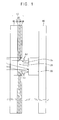
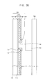
- FIG. 1 is a cross-sectional view of the window structure of FIG. 2 cut along the line I-I'.
- a camera sensor that may be disposed facing the window structure is also shown.
- a window structure 50 may include a window 10, a design layer structure 20 and a light shield layer 30 sequentially stacked on the window 10.
- the design layer structure 20 may include a first design layer 22 and a second design layer 24 sequentially stacked on the window 10, which is a transparent material, e.g., glass, plastic, etc.
- the first and second design layers 22 and 24 may have a chromatic colour or a white colour.
- the design layer structure 20 may have a first hole 25 exposing a top surface of the window 10.
- the first hole 25 may have a step shape of which a diameter may increase from a bottom portion adjacent to the top surface of the window 10 to a top portion distant from the top surface of the window 10.
- the first hole 25 may have a circular shape when view from a top side.
- the light shield layer 30 may have a black colour or a gray colour.
- the light shield layer 30 may have a second hole 35 in fluid communication with, for example aligned with, the first hole 25, and the second hole 35 may have a diameter larger than that of the first hole 25.
- the second hole 35 may have a circular shape when viewed from a top side.
- the first and second holes 25 and 35 may be concentric circles.
- a camera sensor 90 may be disposed facing the first and second holes 25 and 35, and the camera sensor 90 may be disposed on a substrate 80.
- a light that is reflected from an object (not shown) and passes through the window 10 and the first hole 25 of the design layer structure 20 may be incident on the camera sensor 90, and a portion of the light may be reflected from the camera sensor 90 and be incident on the light shield layer 30 and the design layer structure 20.
- a portion of the light incident on the design layer structure 20 may be reflected again (see rays A1 of FIG. 1 ) and be incident on the camera sensor 90.
- the camera sensor 90 may detect a colour of the design layer structure 20 regardless of a colour of the object.
- the portion of the light that is reflected from the object, passes through the window 10 and is incident on the design layer structure 20 may pass through the design layer structure 20 (see rays A2 of FIG. 1 ), and in this case the camera sensor 90 may also detect the colour of the design layer structure 20.
- a light that is incident on a portion of the design layer structure 20 covered by the light shield layer 30 may not pass through the light shield layer 30, and thus may not be incident on the camera sensor 90.
- the colour of the design layer structure 20 may be transferred to surroundings of the image of the object, i.e., a kind of vignette may occur.
- FIG. 3 is a cross sectional view illustrating a window structure in accordance with an exemplary embodiment
- FIG. 4 is a plan view of the window structure of FIG. 3.
- FIG. 3 is a cross-sectional view of the window structure of FIG. 4 cut along the line II-II' of FIG. 4 .
- a camera sensor that may be disposed facing the window structure is also shown.
- a window structure 100 may include a window 110, a first design layer structure 120 and a first light shield layer 130 sequentially stacked on the window 110, and a first light absorption layer 140.
- the window 110 may be a flat plate, and have a first surface 112 and a second surface 114 opposing the first surface 112.
- the window 110 may include a light transmission material, e.g., a synthetic resin such as acryl, or glass.
- the first design layer structure 120 may be formed on the first surface 112 of the window 110.
- the first design layer structure 120 may include a first design layer 122 and a second design layer 124 sequentially stacked on the window 110.
- the first and second design layers 122 and 124 may have a chromatic colour or a white colour.
- the first and second design layers 122 and 124 may have substantially the same colour.
- the first design layer structure 120 may have a first hole 125 exposing a portion of the first surface 112 of the window 110.
- the first hole 125 may have a circular shape when viewed from a top side. Accordingly, as the first design layer structure 120 includes the first and second design layers 122 and 124, the first hole 125 may have a step shape of which a diameter may increase from a bottom portion adjacent to the first surface 112 of the window 110 to a top portion distant from the first surface 112 of the window 110. That is, the second design layer 124 may not cover the whole first design layer 122, and thus the first design layer 122 may be partially exposed.
- FIGS. 3 and 4 show the first design layer structure 120 having the two design layers 122 and 124 sequentially stacked, however, the first design layer structure 120 may have more than two design layers, and the first hole that may be defined as a sidewall and/or a top surface of the design layers may also have a step shape of which a diameter may increase from a bottom portion adjacent to the first surface 112 of the window 110 to a top portion distant from the first surface 112 of the window 110.
- the first design layer structure 120 may have only one design layer.
- the first design structure 120 has two design layers will be illustrated.
- the first light shield layer 130 may have a black colour or a gray or similar colour and be formed on the second design layer 124 of the first design layer structure 120, and have a second hole 135 in fluid communication with the first hole 125.
- the second hole 135 may have a diameter larger than that of the first hole 125.
- the second hole 135 may have a circular shape when viewed from a top side.
- the first and second holes 125 and 135 may be concentric circles.
- the first light shield layer 130 may not cover the whole second design layer 124, and thus the second design layer 124 may be partially exposed.
- a hole structure including the first and second holes 125 and 135 may have a step shape of which a diameter may increase from a bottom portion adjacent to the first surface 112 of the window 110 to a top portion distant from the first surface 112 of the window 110.
- the first light absorption layer 140 may cover at least a portion of the first design layer structure 120 exposed by the first hole structure, i.e., the first and second holes 125 and 135, and may have a third hole 145 exposing a portion of the first surface 112 of the window 110. That is, the first light absorption layer 140 may cover a sidewall of the first design layer 122, a portion of a top surface of the first design layer 122 and a sidewall of the second design layer 124, which may be exposed by the first hole 125 or may define the first hole 125, and a portion of a top surface of the second design layer 124 exposed by the second hole 135.
- the third hole 145 may be formed within the first hole structure consisting of the first and second holes 125 and 135 and may have a diameter that is smaller than that of the first hole structure.
- the third hole 145 and the first hole 125 and/or the second hole 135 may be concentric circles when viewed from a top side.
- the third hole 145 may have a sidewall substantially perpendicular to the first surface 112 of the window 110. That is, the first light absorption layer 140 may have a sidewall substantially perpendicular to the first surface 112 of the window 110.
- the first light absorption layer 140 may cover not only a portion of the first design layer structure 120, but also a sidewall of the first light shield layer 130, which may be exposed by the second hole 135 or may define the second hole 135, and a portion of a top surface of the first light shield layer 130 adjacent to the second hole 135.
- a boundary of the first light absorption layer 140 may be a circle, and the first and second holes 125 and 135 and the boundary of the first light absorption layer 140 may be concentric circles.
- the first light absorption layer 140 may have a top surface substantially parallel to the first surface 112 of the window 110.
- the first light absorption layer 140 may have a black colour or a gray colour.
- the first light shield layer 130 may have a gray colour and the first light absorption layer 140 may have a black colour.
- the first design layer structure 120 and the first light shield layer 130 cover entirely the first surface 112 of the window 110 except for the first to third holes 125, 135 and 145, however, the first design layer structure 120 and the first light shield layer 130 may be formed only at a portion of the first surface 112 of the window 110 adjacent to the first light absorption layer 140 according to a desired design.
- a camera sensor 190 may be disposed facing the third hole 145, and the camera sensor 190 may be disposed on a substrate 180. Accordingly, the third hole 145 may serve as a path through which a light reflected from an object (not shown) may pass.
- a light that is reflected from the object and passes through the window 110 and the third hole 145 may be incident on the camera sensor 190, and a portion of the light may be reflected from the camera sensor 190 and toward the first design layer structure 120, the shield layer 130 or the first light absorption layer 140.
- the first light absorption layer 140 may cover portions of the first design layer structure 120 exposed by the first and second holes 125 and 135, and thus light reflected off the camera sensor 190 may be blocked from being incident on the first design layer structure 120 by the first light absorption layer 140 and the first light shield layer 130.
- the colour of the first design layer structure 120 which may be chromatic or white, may not be detected by the camera sensor 190.
- the first design layer structure 120 may be very thin, a light that is reflected from the object, passes through the window 110 and the first design layer structure 120, and is incident on the first hole 125 or the second hole 135 may be absorbed by the first light absorption layer 140, so that the light may not be incident on the camera sensor 190.
- a light that passes through the window 110 and is incident on a portion of the first design layer structure 120 covered by the first light shield layer 130 may also be blocked by the first light shield layer 130, so that the light that interacts with first design layer structure 120 does not reach camera sensor 190.
- the colour of the first design layer structure 120 that is not related to the colour of the object may be prevented from being incident on the camera sensor 190, and the vignetting, i.e., the colour of the first design layer structure 120 that would otherwise be transferred to surroundings of the image of the object, may be prevented.
- FIG. 5 is a plan view illustrating a window structure in accordance with an exemplary embodiment.
- the window structure may be substantially the same as that of FIGS. 3 and 4 , except for the boundary of the light absorption layer 140.
- like reference numerals refer to like elements, and detailed descriptions thereon are omitted herein.
- a window structure 100 may include a window 110, a first design layer structure 120 and a first light shield layer 130 sequentially stacked on the window 110, and a second light absorption layer 142.
- the second light absorption layer 142 may have a rectangular shaped boundary.
- the window structure 100 may have other types of boundary, e.g., an ellipse, polygon, etc., except for the circle or the rectangle of the first and second light absorption layers 140 and 142, respectively.
- boundary e.g., an ellipse, polygon, etc.
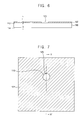
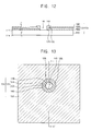
- FIGS. 6-13 FIGS. 6 , 8 , 10 and 12 are cross-sectional views illustrating a method of manufacturing a window structure in accordance with an exemplary embodiment
- FIGS. 7 , 9 , 11 and 13 are plan views of the window structure thereof. More specifically, FIGS. 6 , 8 , 10 and 12 are cross-sectional views of the window structure of FIGS. 7 , 9 , 11 and 13 , respectively, cut along the line III-III' of FIGS. 7 , 9 , 11 and 13 .
- FIGS. 6 to 13 show a method of manufacturing the window structure of FIGS. 3 and 4 , however, these may not be limited thereto.
- the window 110 may include a light transmission material, e.g., a synthetic resin such as acryl, or glass.
- the window 110 may include a first surface 112 and a second surface 114 opposing the first surface 112.
- the first design layer 122 may be formed on the first surface 112 of the window 110.
- the first design layer 122 may be formed by a screen printing process using a mesh. That is, a mesh (not shown) for forming a desired pattern may be mounted on the first surface 112 of the window 110, ink may be sprayed or dropped onto the mesh, and a rubber plate may press the sprayed or dropped ink to form the first design layer 122 having a desired pattern.
- the first design layer 122 may be formed using ink of a chromatic colour or a white colour, and a metal powder, e.g., silver powder may be included in the ink.
- the first design layer 122 may be formed to include a first hole 125 therethrough.
- the first hole 125 may have a circular shape when viewed from a top side.
- a drying process may be further performed after the first design layer 122 is printed on the first surface 112 of the window 110.
- a second design layer 124 may be formed on the first design layer 122.
- the second design layer 124 may be formed by a screen printing process using a mesh as with the first design layer 122.
- the second design layer 124 may be formed using chromatic or white ink, and may be formed using ink having substantially the same colour as that of the first design layer 122.
- the second design layer 124 may be formed to have a hole therethrough.
- the hole in second design layer 124 and the first hole 125 may be concentric circles.
- the hole in second design layer 124 may be in fluid communication with the first hole 125.
- the hole in second design layer 124 may be formed to have a diameter larger than that of the first hole 125 in order for the second design layer 124 may not be formed on a portion of the first surface 112 of the window 110 exposed by the first hole 125 during the screen printing process.
- the first design layer 122 may not be completely covered by the second design layer 124, and a portion of the first design layer 122 adjacent to the first hole 125 may be exposed.
- the first hole 125 through the first design layer 122 together with the hole through the second design layer 124 in fluid communication therewith may be referred to as the first hole 125.
- a bottom of the first hole 125 may be defined by a portion of the first surface 112 of the window 110 not covered by the first design layer 122, and a sidewall of the first hole 125 may be defined by a sidewall and the exposed portion of a top surface of the first design layer 122, and a sidewall of the hole in the second design layer 124.
- the first hole 125 may have a step shape of which a diameter may increase from a bottom portion adjacent to the first surface 112 of the window 110 to a top portion distant from the first surface 112 of the window 110.
- the first and second design layers 122 and 124 may define a first design layer structure 120.
- the first design layer structure 120 may instead be formed to include more than two design layers sequentially stacked, or may not include the second design layer 124 but include only the first design layer 122.
- a first light shield layer 130 may be formed on a top surface of the first design layer structure 120, i.e., on a top surface of the second design layer 124.
- the first light shield layer 130 may be formed by a screen printing process using a mesh as with the first and second design layers 122 and 124.
- the first light shield layer 130 may be formed using black ink or gray ink.
- the first light shield layer 130 may be formed to have a second hole 135 therethrough.
- the second hole 135 may have a circular shape when viewed from a top side.
- the second hole 135 and the first hole 125 may be concentric circles.
- the first and second holes 125 and 135 may be in fluid communication with each other.
- the second hole 135 may be formed to have a diameter larger than that of the first hole 125 so that the first light shield layer 130 may not be formed on the portion of the first surface 112 of the window 110 exposed by the first hole 125. Accordingly, the second design layer 124 may not be completely covered by the first light shield layer 130, and a portion of a top surface of the second design layer 124 adjacent to the first hole 125 may be exposed.
- the first hole 125 together with the second hole 135 in fluid communication therewith may be referred to as a first hole structure.
- a sidewall of the first hole structure may be defined by the sidewall of the first hole 125, the exposed portion of the top surface of the second design layer 124 adjacent to the first hole 125, and a sidewall of the first light shield layer 130.
- the first hole structure may have a step shape of which a diameter may increase from a bottom portion adjacent to the first surface 112 of the window 110 to a top portion distant from the first surface 112 of the window 110.
- a first light absorption layer 140 may be formed on the first surface 112 of the window 110 to cover at least exposed portions of the first design layer structure 120 exposed by the first hole structure, i.e., the first and second holes 125 and 135, and thus the window structure 100 may be manufactured.
- the first light absorption layer 140 may be produced by a screen printing process using a mesh as with the design layers 122 and 124 and the first light shield layer 130.
- the first light absorption layer 140 may be formed using black ink or gray ink.
- the first light absorption layer 140 may have a circular shape when viewed from a top side, and may have a third hole 145 exposing a portion of the first surface 112 of the window 110.
- the first light absorption layer 140 may instead be formed to have other types of shape, e.g., an ellipse, polygon, etc.
- the first light absorption layer 140 may cover at least the sidewall of the first design layer 122, a portion of a top surface of the first design layer 122 and a sidewall of the second design layer 124 that may be exposed by or defining the first hole 125, and a portion of a top surface of the second design layer 124 exposed by the second hole 135. Further, the first light absorption layer 140 may cover a sidewall of the first light absorption layer 130 exposed by or defining the second hole 135 and a portion of a top surface of the first light shield layer 130 adjacent to the second hole 135.
- the third hole 145 may be formed within the first hole structure to have a diameter smaller than that of the first hole structure, and the third hole 145 and the first hole 125 and/or the second hole 135 may be concentric circles.
- the third hole 145 may be formed to have a sidewall substantially perpendicular to the first surface 112 of the window 110. That is, the first light absorption layer 140 may have a sidewall substantially perpendicular to the first surface 112 of the window 110.
- the first light absorption layer 140 may be formed to have a top surface substantially parallel to the first surface 112 of the window 110.
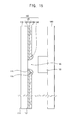
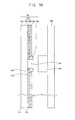
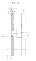
- FIGS. 14 to 19 are cross-sectional views illustrating window structures in accordance with various exemplary embodiments.
- the window structures in FIGS. 14 to 19 may be substantially the same as or similar to that of FIGS. 3 and 4 , except for the shape of the light absorption layer.
- like reference numerals refer to like elements, and detailed descriptions thereof are omitted herein.
- a window structure 100 may include a window 110, a first design layer structure 120 and a first light shield layer 130 sequentially stacked on the window 110, and a third light absorption layer 144.
- the third light absorption layer 144 may have a top surface substantially parallel to the first surface 112 of the window 110, but the third light absorption layer 144 may also have a sidewall that is not perpendicular to the first surface 112 of the window 110, but is instead slanted thereto.
- a third hole 145 of the third light absorption layer 144 may have a diameter that may gradually increase from a bottom portion adjacent to the first surface 112 of the window 110 to a top portion distant from the first surface 112 of the window 110.
- a window structure 100 may include a window 110, a first design layer structure 120 and a first light shield layer 130 sequentially stacked on the window 110, and a fourth light absorption layer 146.
- the fourth light absorption layer 146 may have a curved sidewall that forms various oblique angles with respect to the first surface 112 of the window 110. Furthermore, a top surface of fourth light absorption layer 146 is curved and is therefore not parallel to the first surface 112 of the window 110.
- a window structure 100 may include a window 110, a first design layer structure 120 and a first light shield layer 130 sequentially stacked on the window 110, and a fifth light absorption layer 148.
- the fifth light absorption layer 148 may have a sidewall substantially perpendicular to the first surface 112 of the window 110 and a top surface substantially parallel to the first surface 112 of the window 110, but does not cover a top surface of the first light shield layer 130.
- the fifth light absorption layer 148 may have a top surface substantially higher than that of the first light shield layer 130.
- a window structure 100 may include a window 110, a first design layer structure 120 and a first light shield layer 130 sequentially stacked on the window 110, and a sixth light absorption layer 150.
- the sixth light absorption layer 150 may have a sidewall substantially perpendicular to the first surface 112 of the window 110 and a top surface substantially parallel to the first surface 112 of the window 110, and may be absent from a top surface of the first light shield layer 130 and be substantially coplanar with the top surface of the first light shield layer 130.
- a window structure 100 may include a window 110, a first design layer structure 120 and a first light shield layer 130 sequentially stacked on the window 110, and a seventh light absorption layer 152.
- the seventh light absorption layer 152 may have a curved sidewall slanted with respect to the first surface 112 of the window 110, and may be absent from a top surface of the first light shield layer 130.
- the seventh light absorption layer 152 may have a top surface substantially coplanar with that of the first light shield layer 130.
- a window structure 100 may include a window 110, a first design layer structure 120 and a first light shield layer 130 sequentially stacked on the window 110, and a eighth light absorption layer 154.
- the eighth light absorption layer 154 may have a curved sidewall slanted with respect to the first surface 112 of the window 110, and may be absent from a top surface of the first light shield layer 130.
- the eighth light absorption layer 154 may have a top surface that is lower than that of the first light shield layer 130, and thus may cover only a portion of a sidewall of the first light shield layer 130.
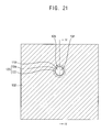
- FIG. 20 is a cross-sectional view illustrating a camera sensor facing a window structure in accordance with an exemplary embodiment and FIG. 21 is a plan view of the window structure of FIG. 20 . More specifically, FIG. 20 is a cross-sectional view of the window structure of FIG. 21 taken along line IV-IV' of FIG. 21 .
- the window structure in FIGS. 20 and 21 may be substantially the same as or similar to that of FIGS. 3 and 4 , except that the window structure may not include a light absorption layer separate from the light shield layer and the light shield layer may have a different shape.
- like reference numerals refer to like elements, and detailed descriptions thereon are omitted herein
- a window structure 100 may include a window 110, and a first design layer structure 120 and a second light shield layer 132 sequentially stacked on the window 110.
- the second light shield layer 132 may cover the first design layer 120 and be formed on the window 110.
- the second light shield layer 132 may have a fourth hole 137 within the first hole 125 that may expose a portion of the first surface 112 of the window 110.
- the fourth hole 137 may have a circular shape when viewed from a top side, and the fourth hole 137 and the first hole 125 may be concentric circles.
- the second light shield layer 132 substantially covers the edges of the design layers 122, 124 that are exposed by the first hole.
- the fourth hole 137 may have a sidewall substantially perpendicular to the first surface 112 of the window 110. That is, the second light shield layer 132 may have a sidewall substantially perpendicular to the first surface 112 of the window 110.
- the second light shield layer 132 may include a black printed layer or a gray printed layer.
- the second light shield layer 132 may cover the first design layer structure 120, and thus light may be prevented from being diffusely reflected at the first design layer structure 120, so that vignetting may be prevented. That is, the second light shield layer 132 may serve as both the light shield layer 130 and the first light absorption layer 140 of the window structure illustrated in FIGS. 3 and 4 .
- FIGS. 22 and 23 are cross-sectional views illustrating window structures in accordance with another example embodiment.
- the window structures in FIGS. 22 and 23 may be substantially the same as or similar to that of FIGS. 20 and 21 , except for the shape of a sidewall of the light shield layer.
- like reference numerals refer to like elements, and detailed descriptions thereon are omitted herein.
- a window structure 100 may include a window 110, a first design layer structure 120 and a third light shield layer 134 sequentially stacked on the window 110.
- the third light shield layer 134 may have a sidewall that is not perpendicular to the first surface 112 of the window 110, but is instead and slanted or oblique thereto. This allows for the amount of light that may be reflected from an outside object, pass through the window 110 and be incident on the camera sensor 190 via the fourth hole 137 to be relatively increased.
- the window structure 100 may instead include a window 110, a first design layer structure 120 and a fourth light shield layer 136 sequentially stacked on the window 110.
- the fourth light shield layer 136 may have a curved sidewall that is not perpendicular to the first surface 112 of the window 110 but is curved.
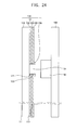
- FIG. 24 is a cross-sectional view illustrating a window structure in accordance with another example embodiment
- FIG. 25 is a plan view of the window structure of FIG. 24
- FIG. 24 a cross-sectional view of the window structure of FIG. 25 cut taken along line V-V' of FIG. 25
- a camera sensor 190 that may be disposed facing the window structure 100 is also shown.
- the window structure 100 in FIG. 24 may be substantially the same as or similar to that of FIGS. 3 and 4 , except for the shape of the design layer structure, the light shield layer and the light absorption layer.
- like reference numerals refer to like elements, and detailed descriptions thereon are omitted herein.
- a window structure 100 may include a window 110, a second design layer structure 121 and a fifth light shield layer 133 sequentially stacked on the window 110, and a ninth light absorption layer 156.
- the second design layer structure 121 may include a first design layer 122 and a third design layer 123 sequentially stacked on the first surface 112 of the window 110.
- the third design layer 123 may entirely cover the first design layer 122.
- a fifth hole 127 of the second design layer structure 121 may have a constant diameter regardless of the distance from the first surface 112 of the window 110.
- the fifth light shield layer 133 may be formed on a top surface of the second design layer structure 121 (i.e., a top surface of the third design layer 123), and may entirely cover the third design layer 123.
- the sixth hole 139 of the fifth light shield layer 133 may have a diameter substantially the same as that of the fifth hole 127.
- a second hole structure including the fifth hole 127 and the sixth hole 139 may have a constant diameter regardless of the distance from the first surface 112 of the window 110.
- the ninth light absorption layer 156 may cover at least a portion of the second design layer structure 121 exposed by the fifth hole 127, i.e., sidewalls of the first and third design layers 122 and 123, and may have a seventh hole 155 exposing a portion of the first surface 112 of the window 110.
- the seventh hole 155 may be formed within the second hole structure including the fifth and sixth holes 127 and 139, and may have a diameter smaller than the second hole structure.
- the seventh hole 155 may have a circular shape when viewed from a top side, and the seventh hole 155 and the fifth hole 127 and/or the sixth hole 139 may be concentric circles.
- the seventh hole 155 may have a sidewall substantially perpendicular to the first surface 112 of the window 110. That is, the ninth light absorption layer 156 may have a sidewall substantially perpendicular to the first surface 112 of the window 110.
- the ninth light absorption layer 156 may cover not only the portion of the second design layer structure 121 but also a sidewall of the fifth light shield layer 133 exposed by or defining the sixth hole 139 and a portion of a top surface of the fifth light shield layer 133 adjacent to the sixth hole 139.
- the ninth light absorption layer 156 may have a boundary of a circle when viewed from a top.
- the boundary of the ninth light absorption layer 156 and the fifth and sixth holes 127 and 139 may be concentric circles.
- the ninth light absorption layer 156 may have a top surface substantially parallel to the first surface 112 of the window 110.
- FIG. 26 is a cross-sectional view illustrating a window structure in accordance with another exemplary embodiment.
- the window structure in FIG. 26 may be substantially the same as or similar to that of FIGS. 3 and 4 , except that the window structure further includes a polyethylene terephthalate (PET) film 170.
- PET polyethylene terephthalate
- a window structure 100 may include a window 110, a PET film 170, a first design layer structure 120 and a first light shield layer 130 sequentially stacked on the PET film 170, and a first light absorption layer 140.
- the first design layer structure 120 may be printed with a high quality and may have a first hole 125 exposing a portion of a top surface of the PET film 170, and the first light shield layer 130 may have a second hole 135 in fluid communication with the first hole 125.
- the first light absorption layer 140 may cover at least a portion of the first design layer structure 120 exposed by the first and second holes 125 and 135, and have a third hole 145 exposing a portion of the top surface of the PET film 170.
- the light transmissive PET film 170 may be formed on the first surface 112 of the window 110, and thus an amount of light incident on the camera sensor 190 may not be affected by PET film 170.
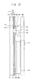
- FIG. 27 is a cross-sectional view illustrating an electronic device equipped with a camera and a window structure in accordance with another exemplary embodiment.
- the electronic device may include the window structure and the camera sensor illustrated with reference to FIGS. 3 and 4 , and thus detailed descriptions thereon are omitted herein.
- the electronic device may include a substrate 180, a display panel 200, a flexible printed circuit board (FPCB) 220, a window structure 100 and a camera sensor 190.
- FPCB flexible printed circuit board
- the substrate 180 may have various types of circuit wirings for driving the electronic device.
- the substrate 180 may be a PCB.
- the display panel 200 may be, e.g., an organic light-emitting diode (OLED) display panel, a liquid crystal display (LCD) panel, or a plasma display panel (PDP), etc.
- OLED organic light-emitting diode
- LCD liquid crystal display
- PDP plasma display panel
- the electronic device may further include a backlight assembly for providing a light to the panels.
- the display panel 200 may be attached to the substrate 180 by an adhesive, e.g., a cushion tape 210.
- the FPCB 220 may include a flexible resin and be connected a surface of the substrate 180 to provide a driving signal to the display panel 200.
- the FPCB 220 may make contact with a first surface of the display panel 200.
- FIG. 27 illustrates that FPBC is bent to contact the second surface of the substrate 180 that faces away from display panel 200, but FPCB 220 may instead be bent to contact a first surface of the substrate 180 that faces the display panel 200.
- the window structure 100 may be formed on a second surface of the display panel 200 opposing the first surface of the display panel 200.
- the window structure 100 may be attached to the display panel 200 by an adhesive, e.g., super view resin (SVR).
- SVR super view resin
- the camera sensor 190 may be disposed facing the third hole 145 of the window structure 100, and may be disposed on the substrate 180 by for example a camera container 185.
- the camera sensor 190 mounted in the electronic device may be disposed facing the third hole 145 of the window structure 100 that includes the first design layer structure 120, and vignetting may be prevent due to the presence of the first light absorption layer 140.
- FIGS. 28 and 29 are cross-sectional views illustrating a method of manufacturing an electronic device equipped with a camera including a window structure in accordance with an exemplary embodiment. More specifically, FIGS. 28 and 29 illustrate a method of manufacturing the electronic device of FIG. 27 .
- FIG. 28 processes substantially the same as or similar to those illustrated with reference to FIGS. 6 to 13 may be performed to manufacture the window structure 100.
- a camera container 185 may be mounted on a first surface of a substrate 180, and a camera sensor 190 may be mounted within the camera container 185. Additionally, a display panel 200 may be attached to the first surface of the substrate 180. In this embodiment, the first surface of the substrate 180 and a first surface of the display panel 200 may be attached to each other by an adhesive, e.g., cushion tape 210.
- an adhesive e.g., cushion tape 210.
- a FPCB 220 may be attached to the first surface of the display panel 200, and be bended to the second surface of the substrate 180 as illustrated in FIG. 29 or to a first surface opposing the first surface of the substrate 180.
- a light transmissive adhesive 230 e.g., SVR may be coated onto the first light shield layer 130 of the window structure 100 so that the window structure 100 may be attached to the second surface of the display panel 200 to manufacture the electronic device.
- the window structure 100 may be attached so that the third hole 145 may face the camera sensor 190 mounted on the substrate 180.
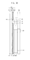
- FIG. 30 is a cross-sectional view illustrating an electronic device equipped with a camera including a window structure in accordance with an exemplary embodiment.
- the electronic device of FIG. 30 may be substantially the same as or similar to that of FIG. 27 , except for the composition of the window structure. That is, the window structure of FIG. 30 does not include the first light absorption layer 140 of FIG. 27 , but instead extends the second light shield layer to cover exposed portions of the first design layer structure 120 so that a vignette image is prevented.
- like reference numerals refer to like elements, and detailed descriptions thereon are omitted herein.
- the window structure in accordance with an exemplary embodiment may be applied to any type of electronic devices having a display panel and a camera.
Landscapes
- Physics & Mathematics (AREA)
- General Physics & Mathematics (AREA)
- Optics & Photonics (AREA)
- Life Sciences & Earth Sciences (AREA)
- Chemical & Material Sciences (AREA)
- Inorganic Chemistry (AREA)
- Sustainable Development (AREA)
- Optical Elements Other Than Lenses (AREA)
- Engineering & Computer Science (AREA)
- Manufacturing & Machinery (AREA)
- Studio Devices (AREA)
Applications Claiming Priority (1)
| Application Number | Priority Date | Filing Date | Title |
|---|---|---|---|
| KR1020120054731A KR102031654B1 (ko) | 2012-05-23 | 2012-05-23 | 윈도우 구조물, 그 제조 방법, 윈도우 구조물을 포함하는 카메라가 탑재된 전자 장치 및 그 제조 방법 |
Publications (2)
| Publication Number | Publication Date |
|---|---|
| EP2667236A1 true EP2667236A1 (fr) | 2013-11-27 |
| EP2667236B1 EP2667236B1 (fr) | 2022-02-02 |
Family
ID=48747295
Family Applications (1)
| Application Number | Title | Priority Date | Filing Date |
|---|---|---|---|
| EP13168002.7A Active EP2667236B1 (fr) | 2012-05-23 | 2013-05-16 | Structure de fenêtre pour dispositif électronique |
Country Status (6)
| Country | Link |
|---|---|
| US (3) | US9640681B2 (fr) |
| EP (1) | EP2667236B1 (fr) |
| JP (1) | JP6247005B2 (fr) |
| KR (1) | KR102031654B1 (fr) |
| CN (3) | CN103424957B (fr) |
| TW (1) | TWI580270B (fr) |
Cited By (9)
| Publication number | Priority date | Publication date | Assignee | Title |
|---|---|---|---|---|
| CN108810197A (zh) * | 2018-05-07 | 2018-11-13 | Oppo广东移动通信有限公司 | 电子装置、盖板组件和显示屏模组 |
| WO2019148931A1 (fr) * | 2018-02-05 | 2019-08-08 | Guangdong Oppo Mobile Telecommunications Corp., Ltd. | Ensemble d'affichage de terminal et terminal mobile |
| WO2019148930A1 (fr) * | 2018-02-05 | 2019-08-08 | Guangdong Oppo Mobile Telecommunications Corp., Ltd. | Ensemble d'affichage de terminal et terminal mobile |
| EP3562129A1 (fr) * | 2018-04-26 | 2019-10-30 | Guangdong Oppo Mobile Telecommunications Corp., Ltd | Ensemble d'affichage de terminal et terminal mobile |
| EP3529648A4 (fr) * | 2016-10-20 | 2020-06-10 | 3M Innovative Properties Company | Camouflage de fenêtre optique d'un dispositif |
| CN111338125A (zh) * | 2018-12-18 | 2020-06-26 | 乐金显示有限公司 | 显示装置 |
| CN113077711A (zh) * | 2020-01-03 | 2021-07-06 | 三星显示有限公司 | 用于显示设备的窗和制造窗的方法 |
| EP4191377A1 (fr) * | 2015-09-28 | 2023-06-07 | Apple Inc. | Dispositif d'affichage de dispositif électronique à zone active étendue |
| US12535719B2 (en) | 2014-02-12 | 2026-01-27 | Semiconductor Energy Laboratory Co., Ltd. | Electronic device with foldable display |
Families Citing this family (55)
| Publication number | Priority date | Publication date | Assignee | Title |
|---|---|---|---|---|
| KR102031654B1 (ko) * | 2012-05-23 | 2019-10-15 | 삼성디스플레이 주식회사 | 윈도우 구조물, 그 제조 방법, 윈도우 구조물을 포함하는 카메라가 탑재된 전자 장치 및 그 제조 방법 |
| CN104635969A (zh) * | 2013-11-14 | 2015-05-20 | 索尼公司 | 触摸屏、电子设备以及防止触摸屏漏光的方法 |
| KR102401285B1 (ko) | 2016-04-01 | 2022-05-24 | 삼성전자주식회사 | 디스플레이를 포함하는 전자 장치 |
| KR102516344B1 (ko) | 2016-06-21 | 2023-04-03 | 삼성전자주식회사 | 커버 윈도우 및 이를 포함하는 전자 장치 |
| US11029558B2 (en) * | 2016-11-07 | 2021-06-08 | Kyocera Corporation | Image display apparatus |
| KR102623993B1 (ko) * | 2016-11-29 | 2024-01-11 | 삼성디스플레이 주식회사 | 데코 필름 및 이를 포함하는 전자 기기 장치 |
| KR102662278B1 (ko) * | 2016-11-30 | 2024-05-02 | 엘지디스플레이 주식회사 | 유기 발광 표시 장치 및 그 제조 방법 |
| KR102301117B1 (ko) * | 2017-03-08 | 2021-09-10 | 삼성전자 주식회사 | 광 센서 모듈을 포함하는 전자 장치 |
| KR102167928B1 (ko) | 2017-03-14 | 2020-10-20 | 엘지전자 주식회사 | 이동 단말기 |
| CN107450253A (zh) * | 2017-07-07 | 2017-12-08 | 瑞声科技(新加坡)有限公司 | 一种压环、该种压环的加工方法以及镜头组件 |
| KR102511474B1 (ko) * | 2017-09-13 | 2023-03-17 | 삼성디스플레이 주식회사 | 표시 장치 |
| CN110021640B (zh) | 2018-01-08 | 2025-02-11 | 三星显示有限公司 | 电致发光装置 |
| KR102572136B1 (ko) | 2018-01-08 | 2023-08-29 | 삼성디스플레이 주식회사 | 윈도우를 갖는 전계 발광 장치 |
| KR102560099B1 (ko) | 2018-03-30 | 2023-07-26 | 삼성디스플레이 주식회사 | 표시 장치 |
| US10983652B2 (en) | 2018-04-13 | 2021-04-20 | Samsung Electronics Co., Ltd. | Display having opaque member disposed in area surrounded by pixels and electronic apparatus having the same |
| CN112041734A (zh) * | 2018-06-13 | 2020-12-04 | Oppo广东移动通信有限公司 | 电子设备的显示组件、电子设备及显示组件的制造方法 |
| CN108881537A (zh) * | 2018-06-22 | 2018-11-23 | Oppo广东移动通信有限公司 | 显示屏组件、电子设备及电子设备的制作方法 |
| CN108957829A (zh) * | 2018-07-06 | 2018-12-07 | Oppo广东移动通信有限公司 | 显示屏组件、电子设备及电子设备的制作方法 |
| KR102626939B1 (ko) * | 2018-10-05 | 2024-01-19 | 삼성디스플레이 주식회사 | 표시 장치 |
| KR102511297B1 (ko) * | 2018-10-05 | 2023-03-17 | 삼성전자주식회사 | 디스플레이 패널 하부에 배치된 센서를 포함하는 전자 장치 |
| KR102653262B1 (ko) | 2018-10-16 | 2024-04-01 | 삼성전자 주식회사 | 개구부가 형성된 터치 레이어를 포함하는 전자 장치 |
| KR102555577B1 (ko) * | 2019-01-28 | 2023-07-18 | 삼성전자주식회사 | 카메라 모듈을 포함하는 전자 장치 |
| CN111510522B (zh) * | 2019-01-31 | 2022-05-06 | 北京小米移动软件有限公司 | 屏幕边框、显示屏模组和终端 |
| KR102756673B1 (ko) | 2019-03-06 | 2025-01-17 | 삼성디스플레이 주식회사 | 표시 장치 |
| CN111726481A (zh) * | 2019-03-19 | 2020-09-29 | 北京小米移动软件有限公司 | 电子设备 |
| US12150338B2 (en) * | 2019-04-30 | 2024-11-19 | Ams Internationalag | OLED display screen including a light absorption layer, and apparatus including such an OLED display screen |
| WO2020222301A1 (fr) * | 2019-05-01 | 2020-11-05 | デクセリアルズ株式会社 | Structure de connexion, procédé de fabrication de structure de connexion, matériau de connexion et particule conductrice revêtue |
| CN110281602B (zh) * | 2019-06-27 | 2021-05-04 | 海宁市金佰利纺织有限公司 | 一种窗帘面料的加工工艺 |
| EP3975539A4 (fr) * | 2019-06-28 | 2022-10-12 | Guangdong Oppo Mobile Telecommunications Corp., Ltd. | Couvercle de diaphragme d'ouverture utilisé pour un module de caméra, ensemble caméra et équipement électronique |
| KR102890704B1 (ko) | 2019-07-02 | 2025-11-27 | 삼성디스플레이 주식회사 | 전자 장치 및 이의 제조 방법 |
| KR102792607B1 (ko) | 2019-07-22 | 2025-04-09 | 삼성디스플레이 주식회사 | 윈도우 부재, 이를 포함하는 전자 장치 및 윈도우 부재의 제조 방법 |
| KR102713286B1 (ko) | 2019-09-06 | 2024-10-04 | 삼성전자 주식회사 | 카메라 모듈을 포함하는 전자 장치 |
| KR102713222B1 (ko) * | 2019-09-06 | 2024-10-07 | 삼성전자 주식회사 | 카메라 모듈을 포함하는 전자 장치 |
| KR102820737B1 (ko) | 2019-10-02 | 2025-06-16 | 삼성디스플레이 주식회사 | 표시 장치 |
| KR102816722B1 (ko) | 2019-10-15 | 2025-06-05 | 삼성디스플레이 주식회사 | 폴더블 표시 장치 |
| KR102950450B1 (ko) | 2019-12-03 | 2026-04-09 | 엘지디스플레이 주식회사 | 디스플레이 장치 |
| KR102830618B1 (ko) | 2019-12-31 | 2025-07-08 | 삼성디스플레이 주식회사 | 표시 장치 |
| KR102797539B1 (ko) * | 2020-02-12 | 2025-04-21 | 삼성디스플레이 주식회사 | 표시 장치 및 전자 기기 |
| US11659653B2 (en) * | 2020-02-14 | 2023-05-23 | Samsung Display Co., Ltd. | Electronic device having window and electronic module disposed under and spaced apart from window |
| KR20210105782A (ko) * | 2020-02-19 | 2021-08-27 | 삼성전자주식회사 | 디스플레이를 포함하는 전자 장치 |
| KR20210109100A (ko) * | 2020-02-26 | 2021-09-06 | 삼성디스플레이 주식회사 | 전자 장치 |
| CN111524451B (zh) | 2020-04-30 | 2022-03-22 | 昆山国显光电有限公司 | 显示面板及显示装置 |
| CN111584567B (zh) * | 2020-05-11 | 2022-08-23 | 武汉华星光电半导体显示技术有限公司 | 显示装置及其制备方法 |
| CN111627317A (zh) * | 2020-05-18 | 2020-09-04 | 武汉华星光电半导体显示技术有限公司 | 显示装置及其制作方法 |
| KR102448029B1 (ko) | 2020-06-11 | 2022-09-28 | 삼성디스플레이 주식회사 | 표시 장치 |
| KR102865252B1 (ko) | 2020-07-21 | 2025-09-30 | 삼성전자 주식회사 | 카메라 구조체 및 카메라 구조체를 포함하는 전자 장치 |
| KR102870765B1 (ko) | 2020-07-31 | 2025-10-16 | 삼성디스플레이 주식회사 | 전자 장치 |
| KR102886676B1 (ko) * | 2020-09-10 | 2025-11-14 | 삼성전자주식회사 | 디스플레이의 적어도 일부를 통해 촬영을 수행하는 카메라 모듈을 포함하는 전자 장치 |
| CN112396956A (zh) * | 2020-11-05 | 2021-02-23 | 武汉华星光电半导体显示技术有限公司 | 一种显示面板和显示装置 |
| KR102886907B1 (ko) | 2020-12-29 | 2025-11-18 | 삼성디스플레이 주식회사 | 전자 장치 |
| KR20220110396A (ko) | 2021-01-29 | 2022-08-08 | 삼성디스플레이 주식회사 | 디스플레이 장치 |
| KR20220115709A (ko) | 2021-02-09 | 2022-08-18 | 삼성디스플레이 주식회사 | 표시 패널 및 이를 구비하는 표시 장치 |
| EP4277244B1 (fr) | 2021-06-04 | 2025-11-12 | Samsung Electronics Co., Ltd. | Dispositif électronique comprenant une fenêtre pour module optique |
| KR20240054475A (ko) | 2022-10-18 | 2024-04-26 | 삼성디스플레이 주식회사 | 표시 패널 및 이를 포함하는 전자 기기 |
| WO2025220987A1 (fr) * | 2024-04-15 | 2025-10-23 | 삼성전자 주식회사 | Boitier et dispositif électronique pouvant être porté le comprenant |
Citations (2)
| Publication number | Priority date | Publication date | Assignee | Title |
|---|---|---|---|---|
| US20060051085A1 (en) * | 2004-09-03 | 2006-03-09 | Fujinon Corporation | Diaphragm |
| US20110141336A1 (en) * | 2009-12-11 | 2011-06-16 | Apple Inc. | Photochromatic coating for controlling lens flare |
Family Cites Families (26)
| Publication number | Priority date | Publication date | Assignee | Title |
|---|---|---|---|---|
| USH654H (en) | 1988-05-26 | 1989-07-04 | Polaroid Corporation | Positive vignetting accessory |
| JP2001111873A (ja) * | 1999-10-12 | 2001-04-20 | Sony Corp | 撮像装置及びカメラシステム |
| US7027683B2 (en) * | 2000-08-15 | 2006-04-11 | Nanostream, Inc. | Optical devices with fluidic systems |
| US7049528B2 (en) * | 2002-02-06 | 2006-05-23 | Ibiden Co., Ltd. | Semiconductor chip mounting wiring board, manufacturing method for same, and semiconductor module |
| JP2003274234A (ja) * | 2002-03-15 | 2003-09-26 | Casio Comput Co Ltd | 撮像機器 |
| JP4189184B2 (ja) | 2002-08-28 | 2008-12-03 | Hoya株式会社 | 電子スチルカメラ |
| JP4526776B2 (ja) | 2003-04-02 | 2010-08-18 | 株式会社半導体エネルギー研究所 | 発光装置及び電子機器 |
| JP4365743B2 (ja) | 2004-07-27 | 2009-11-18 | 富士通マイクロエレクトロニクス株式会社 | 撮像装置 |
| US20070133983A1 (en) * | 2005-12-14 | 2007-06-14 | Matilda Traff | Light-controlling element for a camera |
| JP2008166632A (ja) | 2006-12-29 | 2008-07-17 | Manabu Bonshihara | 固体撮像装置及びその製造方法並びにカメラモジュール |
| US7867793B2 (en) | 2007-07-09 | 2011-01-11 | Koninklijke Philips Electronics N.V. | Substrate removal during LED formation |
| ES2630408T3 (es) * | 2008-12-01 | 2017-08-21 | Lg Electronics Inc. | Procedimiento de operación de un icono de ejecución de terminal móvil |
| TW201033707A (en) * | 2009-03-04 | 2010-09-16 | Au Optronics Corp | Flat display panel |
| KR20100112413A (ko) * | 2009-04-09 | 2010-10-19 | 엘지전자 주식회사 | 디스플레이 장치 |
| JP2011097026A (ja) * | 2009-09-30 | 2011-05-12 | Sanyo Electric Co Ltd | 素子搭載用基板、半導体モジュール、光学モジュールおよびカメラモジュール |
| KR100989020B1 (ko) | 2010-03-23 | 2010-10-20 | 이창일 | 적외선 감시카메라용 윈도우 |
| US8610822B2 (en) * | 2010-04-19 | 2013-12-17 | Apple Inc. | Camera alignment and mounting structures |
| TWI462067B (zh) * | 2010-04-27 | 2014-11-21 | Lg Display Co Ltd | 顯示設備 |
| KR101661659B1 (ko) | 2010-07-07 | 2016-09-30 | 엘지이노텍 주식회사 | 소형 카메라 모듈용 후드 유닛 및 상기 후드 유닛이 장착된 장치 |
| JP2012019382A (ja) * | 2010-07-08 | 2012-01-26 | Sony Corp | 電子機器 |
| DE102011052540B4 (de) * | 2010-08-11 | 2017-10-26 | Corning Precision Materials Co., Ltd. | Mehrschichtiger Gegenstand und Verfahren zu seiner Herstellung |
| KR101232763B1 (ko) | 2010-09-01 | 2013-02-13 | 유한회사 마스터이미지쓰리디아시아 | 서브 셀 요소 단위 패럴랙스 배리어 방식 입체영상 표시 장치 |
| US8642119B2 (en) * | 2010-09-22 | 2014-02-04 | Stmicroelectronics Pte Ltd. | Method and system for shielding semiconductor devices from light |
| US8567955B2 (en) * | 2011-03-24 | 2013-10-29 | Apple Inc. | Methods and apparatus for concealing sensors and other components of electronic devices |
| US20130286282A1 (en) * | 2012-04-27 | 2013-10-31 | Toppan Printing Co., Ltd. | Camera Module and Manufacturing Method Thereof |
| KR102031654B1 (ko) | 2012-05-23 | 2019-10-15 | 삼성디스플레이 주식회사 | 윈도우 구조물, 그 제조 방법, 윈도우 구조물을 포함하는 카메라가 탑재된 전자 장치 및 그 제조 방법 |
-
2012
- 2012-05-23 KR KR1020120054731A patent/KR102031654B1/ko active Active
-
2013
- 2013-01-23 JP JP2013010361A patent/JP6247005B2/ja active Active
- 2013-03-12 US US13/797,696 patent/US9640681B2/en active Active
- 2013-05-13 TW TW102116830A patent/TWI580270B/zh active
- 2013-05-16 EP EP13168002.7A patent/EP2667236B1/fr active Active
- 2013-05-16 CN CN201310181276.XA patent/CN103424957B/zh active Active
- 2013-05-16 CN CN201320582392.8U patent/CN203688963U/zh not_active Expired - Lifetime
- 2013-05-16 CN CN2013202670511U patent/CN203337980U/zh not_active Expired - Lifetime
-
2017
- 2017-03-13 US US15/457,563 patent/US10134922B2/en active Active
-
2018
- 2018-11-19 US US16/195,327 patent/US20190123218A1/en not_active Abandoned
Patent Citations (2)
| Publication number | Priority date | Publication date | Assignee | Title |
|---|---|---|---|---|
| US20060051085A1 (en) * | 2004-09-03 | 2006-03-09 | Fujinon Corporation | Diaphragm |
| US20110141336A1 (en) * | 2009-12-11 | 2011-06-16 | Apple Inc. | Photochromatic coating for controlling lens flare |
Cited By (16)
| Publication number | Priority date | Publication date | Assignee | Title |
|---|---|---|---|---|
| US12535719B2 (en) | 2014-02-12 | 2026-01-27 | Semiconductor Energy Laboratory Co., Ltd. | Electronic device with foldable display |
| US12183307B2 (en) | 2015-09-28 | 2024-12-31 | Apple Inc. | Electronic device display with extended active area |
| US11823645B2 (en) | 2015-09-28 | 2023-11-21 | Apple Inc. | Electronic device display with extended active area |
| EP4191377A1 (fr) * | 2015-09-28 | 2023-06-07 | Apple Inc. | Dispositif d'affichage de dispositif électronique à zone active étendue |
| EP3529648A4 (fr) * | 2016-10-20 | 2020-06-10 | 3M Innovative Properties Company | Camouflage de fenêtre optique d'un dispositif |
| US10917506B2 (en) | 2018-02-05 | 2021-02-09 | Guangdong Oppo Mobile Telecommunications Corp., Ltd. | Terminal display assembly and mobile terminal |
| WO2019148931A1 (fr) * | 2018-02-05 | 2019-08-08 | Guangdong Oppo Mobile Telecommunications Corp., Ltd. | Ensemble d'affichage de terminal et terminal mobile |
| WO2019148930A1 (fr) * | 2018-02-05 | 2019-08-08 | Guangdong Oppo Mobile Telecommunications Corp., Ltd. | Ensemble d'affichage de terminal et terminal mobile |
| US10620665B2 (en) | 2018-02-05 | 2020-04-14 | Guangdong Oppo Mobile Telecommunications Corp., Lt | Terminal display assembly and mobile terminal |
| US10855822B2 (en) | 2018-04-26 | 2020-12-01 | Guangdong Oppo Mobile Telecommunications Corp., Ltd. | Terminal display assembly and mobile terminal |
| EP3562129A1 (fr) * | 2018-04-26 | 2019-10-30 | Guangdong Oppo Mobile Telecommunications Corp., Ltd | Ensemble d'affichage de terminal et terminal mobile |
| CN108810197A (zh) * | 2018-05-07 | 2018-11-13 | Oppo广东移动通信有限公司 | 电子装置、盖板组件和显示屏模组 |
| CN108810197B (zh) * | 2018-05-07 | 2020-05-12 | Oppo广东移动通信有限公司 | 电子装置、盖板组件和显示屏模组 |
| CN111338125B (zh) * | 2018-12-18 | 2023-11-03 | 乐金显示有限公司 | 显示装置 |
| CN111338125A (zh) * | 2018-12-18 | 2020-06-26 | 乐金显示有限公司 | 显示装置 |
| CN113077711A (zh) * | 2020-01-03 | 2021-07-06 | 三星显示有限公司 | 用于显示设备的窗和制造窗的方法 |
Also Published As
| Publication number | Publication date |
|---|---|
| US20130313672A1 (en) | 2013-11-28 |
| CN203337980U (zh) | 2013-12-11 |
| CN103424957A (zh) | 2013-12-04 |
| EP2667236B1 (fr) | 2022-02-02 |
| TW201401862A (zh) | 2014-01-01 |
| US10134922B2 (en) | 2018-11-20 |
| CN203688963U (zh) | 2014-07-02 |
| KR102031654B1 (ko) | 2019-10-15 |
| KR20130131017A (ko) | 2013-12-03 |
| US9640681B2 (en) | 2017-05-02 |
| JP6247005B2 (ja) | 2017-12-13 |
| TWI580270B (zh) | 2017-04-21 |
| CN103424957B (zh) | 2018-08-10 |
| US20190123218A1 (en) | 2019-04-25 |
| JP2013247672A (ja) | 2013-12-09 |
| US20170186891A1 (en) | 2017-06-29 |
Similar Documents
| Publication | Publication Date | Title |
|---|---|---|
| EP2667236B1 (fr) | Structure de fenêtre pour dispositif électronique | |
| US8366286B2 (en) | Light-transmissive input device and method of manufacturing the same | |
| US11023010B2 (en) | Panel bottom sheet and display device including the same | |
| CN108615749B (zh) | 发光模组及显示装置 | |
| KR102522575B1 (ko) | 윈도우 부재 및 표시 장치의 제조 방법 | |
| US11006525B2 (en) | Display device and method of manufacturing the same | |
| US20190037063A1 (en) | Display panel and electronic device | |
| US9832890B2 (en) | Cover window, method of manufacturing the cover window, and display device including the cover window | |
| JP2012098785A (ja) | 入力装置の製造方法 | |
| JP2009251550A (ja) | 電気光学装置、入力装置及び電子機器 | |
| US20180198089A1 (en) | Display device | |
| KR102443605B1 (ko) | 표시 장치용 커버 윈도우 및 그 제조 방법 | |
| CN105302377B (zh) | 保护盖板及应用其的触控装置 | |
| KR20130128711A (ko) | 터치 패널 및 그 제조 방법 | |
| EP3686709B1 (fr) | Appareil électronique et procédé d'assemblage de module d'empreinte digitale | |
| US12212828B2 (en) | Electrical charge discharging pattern and electronic device including the same | |
| EP3104217B1 (fr) | Dispositif mobile comprenant module d'affichage à cristaux liquides | |
| JP3201084U (ja) | 面状発光装置 | |
| US20260063960A1 (en) | Display device | |
| US11667014B2 (en) | Jig for cover window | |
| US20230288746A1 (en) | Electronic device and manufacturing method thereof | |
| JP2011008666A (ja) | 座標入力装置とそれを備えた表示装置及び電子機器 | |
| CN112416167A (zh) | 触控显示模组及电子设备 |
Legal Events
| Date | Code | Title | Description |
|---|---|---|---|
| PUAI | Public reference made under article 153(3) epc to a published international application that has entered the european phase |
Free format text: ORIGINAL CODE: 0009012 |
|
| AK | Designated contracting states |
Kind code of ref document: A1 Designated state(s): AL AT BE BG CH CY CZ DE DK EE ES FI FR GB GR HR HU IE IS IT LI LT LU LV MC MK MT NL NO PL PT RO RS SE SI SK SM TR |
|
| AX | Request for extension of the european patent |
Extension state: BA ME |
|
| 17P | Request for examination filed |
Effective date: 20140527 |
|
| RBV | Designated contracting states (corrected) |
Designated state(s): AL AT BE BG CH CY CZ DE DK EE ES FI FR GB GR HR HU IE IS IT LI LT LU LV MC MK MT NL NO PL PT RO RS SE SI SK SM TR |
|
| RIN1 | Information on inventor provided before grant (corrected) |
Inventor name: MIN, MYUNG-AN |
|
| RAP1 | Party data changed (applicant data changed or rights of an application transferred) |
Owner name: SAMSUNG DISPLAY CO., LTD. |
|
| STAA | Information on the status of an ep patent application or granted ep patent |
Free format text: STATUS: EXAMINATION IS IN PROGRESS |
|
| 17Q | First examination report despatched |
Effective date: 20170915 |
|
| GRAP | Despatch of communication of intention to grant a patent |
Free format text: ORIGINAL CODE: EPIDOSNIGR1 |
|
| STAA | Information on the status of an ep patent application or granted ep patent |
Free format text: STATUS: GRANT OF PATENT IS INTENDED |
|
| INTG | Intention to grant announced |
Effective date: 20210929 |
|
| GRAS | Grant fee paid |
Free format text: ORIGINAL CODE: EPIDOSNIGR3 |
|
| GRAA | (expected) grant |
Free format text: ORIGINAL CODE: 0009210 |
|
| STAA | Information on the status of an ep patent application or granted ep patent |
Free format text: STATUS: THE PATENT HAS BEEN GRANTED |
|
| AK | Designated contracting states |
Kind code of ref document: B1 Designated state(s): AL AT BE BG CH CY CZ DE DK EE ES FI FR GB GR HR HU IE IS IT LI LT LU LV MC MK MT NL NO PL PT RO RS SE SI SK SM TR |
|
| REG | Reference to a national code |
Ref country code: GB Ref legal event code: FG4D |
|
| REG | Reference to a national code |
Ref country code: CH Ref legal event code: EP Ref country code: AT Ref legal event code: REF Ref document number: 1466737 Country of ref document: AT Kind code of ref document: T Effective date: 20220215 |
|
| REG | Reference to a national code |
Ref country code: DE Ref legal event code: R096 Ref document number: 602013080833 Country of ref document: DE |
|
| REG | Reference to a national code |
Ref country code: IE Ref legal event code: FG4D |
|
| REG | Reference to a national code |
Ref country code: NL Ref legal event code: FP |
|
| REG | Reference to a national code |
Ref country code: LT Ref legal event code: MG9D |
|
| REG | Reference to a national code |
Ref country code: AT Ref legal event code: MK05 Ref document number: 1466737 Country of ref document: AT Kind code of ref document: T Effective date: 20220202 |
|
| PG25 | Lapsed in a contracting state [announced via postgrant information from national office to epo] |
Ref country code: SE Free format text: LAPSE BECAUSE OF FAILURE TO SUBMIT A TRANSLATION OF THE DESCRIPTION OR TO PAY THE FEE WITHIN THE PRESCRIBED TIME-LIMIT Effective date: 20220202 Ref country code: RS Free format text: LAPSE BECAUSE OF FAILURE TO SUBMIT A TRANSLATION OF THE DESCRIPTION OR TO PAY THE FEE WITHIN THE PRESCRIBED TIME-LIMIT Effective date: 20220202 Ref country code: PT Free format text: LAPSE BECAUSE OF FAILURE TO SUBMIT A TRANSLATION OF THE DESCRIPTION OR TO PAY THE FEE WITHIN THE PRESCRIBED TIME-LIMIT Effective date: 20220602 Ref country code: NO Free format text: LAPSE BECAUSE OF FAILURE TO SUBMIT A TRANSLATION OF THE DESCRIPTION OR TO PAY THE FEE WITHIN THE PRESCRIBED TIME-LIMIT Effective date: 20220502 Ref country code: LT Free format text: LAPSE BECAUSE OF FAILURE TO SUBMIT A TRANSLATION OF THE DESCRIPTION OR TO PAY THE FEE WITHIN THE PRESCRIBED TIME-LIMIT Effective date: 20220202 Ref country code: HR Free format text: LAPSE BECAUSE OF FAILURE TO SUBMIT A TRANSLATION OF THE DESCRIPTION OR TO PAY THE FEE WITHIN THE PRESCRIBED TIME-LIMIT Effective date: 20220202 Ref country code: ES Free format text: LAPSE BECAUSE OF FAILURE TO SUBMIT A TRANSLATION OF THE DESCRIPTION OR TO PAY THE FEE WITHIN THE PRESCRIBED TIME-LIMIT Effective date: 20220202 Ref country code: BG Free format text: LAPSE BECAUSE OF FAILURE TO SUBMIT A TRANSLATION OF THE DESCRIPTION OR TO PAY THE FEE WITHIN THE PRESCRIBED TIME-LIMIT Effective date: 20220502 |
|
| PG25 | Lapsed in a contracting state [announced via postgrant information from national office to epo] |
Ref country code: PL Free format text: LAPSE BECAUSE OF FAILURE TO SUBMIT A TRANSLATION OF THE DESCRIPTION OR TO PAY THE FEE WITHIN THE PRESCRIBED TIME-LIMIT Effective date: 20220202 Ref country code: LV Free format text: LAPSE BECAUSE OF FAILURE TO SUBMIT A TRANSLATION OF THE DESCRIPTION OR TO PAY THE FEE WITHIN THE PRESCRIBED TIME-LIMIT Effective date: 20220202 Ref country code: GR Free format text: LAPSE BECAUSE OF FAILURE TO SUBMIT A TRANSLATION OF THE DESCRIPTION OR TO PAY THE FEE WITHIN THE PRESCRIBED TIME-LIMIT Effective date: 20220503 Ref country code: FI Free format text: LAPSE BECAUSE OF FAILURE TO SUBMIT A TRANSLATION OF THE DESCRIPTION OR TO PAY THE FEE WITHIN THE PRESCRIBED TIME-LIMIT Effective date: 20220202 Ref country code: AT Free format text: LAPSE BECAUSE OF FAILURE TO SUBMIT A TRANSLATION OF THE DESCRIPTION OR TO PAY THE FEE WITHIN THE PRESCRIBED TIME-LIMIT Effective date: 20220202 |
|
| PG25 | Lapsed in a contracting state [announced via postgrant information from national office to epo] |
Ref country code: IS Free format text: LAPSE BECAUSE OF FAILURE TO SUBMIT A TRANSLATION OF THE DESCRIPTION OR TO PAY THE FEE WITHIN THE PRESCRIBED TIME-LIMIT Effective date: 20220602 |
|
| PG25 | Lapsed in a contracting state [announced via postgrant information from national office to epo] |
Ref country code: SM Free format text: LAPSE BECAUSE OF FAILURE TO SUBMIT A TRANSLATION OF THE DESCRIPTION OR TO PAY THE FEE WITHIN THE PRESCRIBED TIME-LIMIT Effective date: 20220202 Ref country code: SK Free format text: LAPSE BECAUSE OF FAILURE TO SUBMIT A TRANSLATION OF THE DESCRIPTION OR TO PAY THE FEE WITHIN THE PRESCRIBED TIME-LIMIT Effective date: 20220202 Ref country code: RO Free format text: LAPSE BECAUSE OF FAILURE TO SUBMIT A TRANSLATION OF THE DESCRIPTION OR TO PAY THE FEE WITHIN THE PRESCRIBED TIME-LIMIT Effective date: 20220202 Ref country code: EE Free format text: LAPSE BECAUSE OF FAILURE TO SUBMIT A TRANSLATION OF THE DESCRIPTION OR TO PAY THE FEE WITHIN THE PRESCRIBED TIME-LIMIT Effective date: 20220202 Ref country code: DK Free format text: LAPSE BECAUSE OF FAILURE TO SUBMIT A TRANSLATION OF THE DESCRIPTION OR TO PAY THE FEE WITHIN THE PRESCRIBED TIME-LIMIT Effective date: 20220202 Ref country code: CZ Free format text: LAPSE BECAUSE OF FAILURE TO SUBMIT A TRANSLATION OF THE DESCRIPTION OR TO PAY THE FEE WITHIN THE PRESCRIBED TIME-LIMIT Effective date: 20220202 |
|
| REG | Reference to a national code |
Ref country code: DE Ref legal event code: R097 Ref document number: 602013080833 Country of ref document: DE |
|
| PG25 | Lapsed in a contracting state [announced via postgrant information from national office to epo] |
Ref country code: AL Free format text: LAPSE BECAUSE OF FAILURE TO SUBMIT A TRANSLATION OF THE DESCRIPTION OR TO PAY THE FEE WITHIN THE PRESCRIBED TIME-LIMIT Effective date: 20220202 |
|
| PLBE | No opposition filed within time limit |
Free format text: ORIGINAL CODE: 0009261 |
|
| STAA | Information on the status of an ep patent application or granted ep patent |
Free format text: STATUS: NO OPPOSITION FILED WITHIN TIME LIMIT |
|
| REG | Reference to a national code |
Ref country code: CH Ref legal event code: PL |
|
| 26N | No opposition filed |
Effective date: 20221103 |
|
| REG | Reference to a national code |
Ref country code: BE Ref legal event code: MM Effective date: 20220531 |
|
| PG25 | Lapsed in a contracting state [announced via postgrant information from national office to epo] |
Ref country code: MC Free format text: LAPSE BECAUSE OF FAILURE TO SUBMIT A TRANSLATION OF THE DESCRIPTION OR TO PAY THE FEE WITHIN THE PRESCRIBED TIME-LIMIT Effective date: 20220202 Ref country code: LU Free format text: LAPSE BECAUSE OF NON-PAYMENT OF DUE FEES Effective date: 20220516 Ref country code: LI Free format text: LAPSE BECAUSE OF NON-PAYMENT OF DUE FEES Effective date: 20220531 Ref country code: CH Free format text: LAPSE BECAUSE OF NON-PAYMENT OF DUE FEES Effective date: 20220531 |
|
| PG25 | Lapsed in a contracting state [announced via postgrant information from national office to epo] |
Ref country code: SI Free format text: LAPSE BECAUSE OF FAILURE TO SUBMIT A TRANSLATION OF THE DESCRIPTION OR TO PAY THE FEE WITHIN THE PRESCRIBED TIME-LIMIT Effective date: 20220202 |
|
| PG25 | Lapsed in a contracting state [announced via postgrant information from national office to epo] |
Ref country code: IE Free format text: LAPSE BECAUSE OF NON-PAYMENT OF DUE FEES Effective date: 20220516 |
|
| PG25 | Lapsed in a contracting state [announced via postgrant information from national office to epo] |
Ref country code: BE Free format text: LAPSE BECAUSE OF NON-PAYMENT OF DUE FEES Effective date: 20220531 |
|
| P01 | Opt-out of the competence of the unified patent court (upc) registered |
Effective date: 20230515 |
|
| PG25 | Lapsed in a contracting state [announced via postgrant information from national office to epo] |
Ref country code: IT Free format text: LAPSE BECAUSE OF FAILURE TO SUBMIT A TRANSLATION OF THE DESCRIPTION OR TO PAY THE FEE WITHIN THE PRESCRIBED TIME-LIMIT Effective date: 20220202 |
|
| PG25 | Lapsed in a contracting state [announced via postgrant information from national office to epo] |
Ref country code: HU Free format text: LAPSE BECAUSE OF FAILURE TO SUBMIT A TRANSLATION OF THE DESCRIPTION OR TO PAY THE FEE WITHIN THE PRESCRIBED TIME-LIMIT; INVALID AB INITIO Effective date: 20130516 |
|
| PG25 | Lapsed in a contracting state [announced via postgrant information from national office to epo] |
Ref country code: MK Free format text: LAPSE BECAUSE OF FAILURE TO SUBMIT A TRANSLATION OF THE DESCRIPTION OR TO PAY THE FEE WITHIN THE PRESCRIBED TIME-LIMIT Effective date: 20220202 Ref country code: CY Free format text: LAPSE BECAUSE OF FAILURE TO SUBMIT A TRANSLATION OF THE DESCRIPTION OR TO PAY THE FEE WITHIN THE PRESCRIBED TIME-LIMIT Effective date: 20220202 |
|
| PG25 | Lapsed in a contracting state [announced via postgrant information from national office to epo] |
Ref country code: TR Free format text: LAPSE BECAUSE OF FAILURE TO SUBMIT A TRANSLATION OF THE DESCRIPTION OR TO PAY THE FEE WITHIN THE PRESCRIBED TIME-LIMIT Effective date: 20220202 |
|
| PG25 | Lapsed in a contracting state [announced via postgrant information from national office to epo] |
Ref country code: MT Free format text: LAPSE BECAUSE OF FAILURE TO SUBMIT A TRANSLATION OF THE DESCRIPTION OR TO PAY THE FEE WITHIN THE PRESCRIBED TIME-LIMIT Effective date: 20220202 |
|
| PGFP | Annual fee paid to national office [announced via postgrant information from national office to epo] |
Ref country code: NL Payment date: 20250422 Year of fee payment: 13 |
|
| PGFP | Annual fee paid to national office [announced via postgrant information from national office to epo] |
Ref country code: DE Payment date: 20250422 Year of fee payment: 13 |
|
| PGFP | Annual fee paid to national office [announced via postgrant information from national office to epo] |
Ref country code: FR Payment date: 20250422 Year of fee payment: 13 |
|
| PGFP | Annual fee paid to national office [announced via postgrant information from national office to epo] |
Ref country code: GB Payment date: 20260324 Year of fee payment: 14 |