EP2667247B1 - Appareil d'affichage à cristaux liquides - Google Patents
Appareil d'affichage à cristaux liquides Download PDFInfo
- Publication number
- EP2667247B1 EP2667247B1 EP13168931.7A EP13168931A EP2667247B1 EP 2667247 B1 EP2667247 B1 EP 2667247B1 EP 13168931 A EP13168931 A EP 13168931A EP 2667247 B1 EP2667247 B1 EP 2667247B1
- Authority
- EP
- European Patent Office
- Prior art keywords
- liquid crystal
- display apparatus
- crystal display
- reinforcing member
- strength reinforcing
- Prior art date
- Legal status (The legal status is an assumption and is not a legal conclusion. Google has not performed a legal analysis and makes no representation as to the accuracy of the status listed.)
- Active
Links
Images


Classifications
-
- G—PHYSICS
- G02—OPTICS
- G02F—OPTICAL DEVICES OR ARRANGEMENTS FOR THE CONTROL OF LIGHT BY MODIFICATION OF THE OPTICAL PROPERTIES OF THE MEDIA OF THE ELEMENTS INVOLVED THEREIN; NON-LINEAR OPTICS; FREQUENCY-CHANGING OF LIGHT; OPTICAL LOGIC ELEMENTS; OPTICAL ANALOGUE/DIGITAL CONVERTERS
- G02F1/00—Devices or arrangements for the control of the intensity, colour, phase, polarisation or direction of light arriving from an independent light source, e.g. switching, gating or modulating; Non-linear optics
- G02F1/01—Devices or arrangements for the control of the intensity, colour, phase, polarisation or direction of light arriving from an independent light source, e.g. switching, gating or modulating; Non-linear optics for the control of the intensity, phase, polarisation or colour
- G02F1/13—Devices or arrangements for the control of the intensity, colour, phase, polarisation or direction of light arriving from an independent light source, e.g. switching, gating or modulating; Non-linear optics for the control of the intensity, phase, polarisation or colour based on liquid crystals, e.g. single liquid crystal display cells
- G02F1/133—Constructional arrangements; Operation of liquid crystal cells; Circuit arrangements
- G02F1/1333—Constructional arrangements; Manufacturing methods
- G02F1/1335—Structural association of cells with optical devices, e.g. polarisers or reflectors
- G02F1/1336—Illuminating devices
- G02F1/133602—Direct backlight
- G02F1/133608—Direct backlight including particular frames or supporting means
-
- G—PHYSICS
- G02—OPTICS
- G02F—OPTICAL DEVICES OR ARRANGEMENTS FOR THE CONTROL OF LIGHT BY MODIFICATION OF THE OPTICAL PROPERTIES OF THE MEDIA OF THE ELEMENTS INVOLVED THEREIN; NON-LINEAR OPTICS; FREQUENCY-CHANGING OF LIGHT; OPTICAL LOGIC ELEMENTS; OPTICAL ANALOGUE/DIGITAL CONVERTERS
- G02F1/00—Devices or arrangements for the control of the intensity, colour, phase, polarisation or direction of light arriving from an independent light source, e.g. switching, gating or modulating; Non-linear optics
- G02F1/01—Devices or arrangements for the control of the intensity, colour, phase, polarisation or direction of light arriving from an independent light source, e.g. switching, gating or modulating; Non-linear optics for the control of the intensity, phase, polarisation or colour
- G02F1/13—Devices or arrangements for the control of the intensity, colour, phase, polarisation or direction of light arriving from an independent light source, e.g. switching, gating or modulating; Non-linear optics for the control of the intensity, phase, polarisation or colour based on liquid crystals, e.g. single liquid crystal display cells
- G02F1/133—Constructional arrangements; Operation of liquid crystal cells; Circuit arrangements
- G02F1/1333—Constructional arrangements; Manufacturing methods
- G02F1/133308—Support structures for LCD panels, e.g. frames or bezels
-
- G—PHYSICS
- G02—OPTICS
- G02B—OPTICAL ELEMENTS, SYSTEMS OR APPARATUS
- G02B6/00—Light guides; Structural details of arrangements comprising light guides and other optical elements, e.g. couplings
- G02B6/0001—Light guides; Structural details of arrangements comprising light guides and other optical elements, e.g. couplings specially adapted for lighting devices or systems
- G02B6/0011—Light guides; Structural details of arrangements comprising light guides and other optical elements, e.g. couplings specially adapted for lighting devices or systems the light guides being planar or of plate-like form
- G02B6/0081—Mechanical or electrical aspects of the light guide and light source in the lighting device peculiar to the adaptation to planar light guides, e.g. concerning packaging
- G02B6/0093—Means for protecting the light guide
-
- G—PHYSICS
- G02—OPTICS
- G02B—OPTICAL ELEMENTS, SYSTEMS OR APPARATUS
- G02B6/00—Light guides; Structural details of arrangements comprising light guides and other optical elements, e.g. couplings
- G02B6/0001—Light guides; Structural details of arrangements comprising light guides and other optical elements, e.g. couplings specially adapted for lighting devices or systems
- G02B6/0011—Light guides; Structural details of arrangements comprising light guides and other optical elements, e.g. couplings specially adapted for lighting devices or systems the light guides being planar or of plate-like form
- G02B6/0081—Mechanical or electrical aspects of the light guide and light source in the lighting device peculiar to the adaptation to planar light guides, e.g. concerning packaging
- G02B6/0085—Means for removing heat created by the light source from the package
-
- G—PHYSICS
- G02—OPTICS
- G02F—OPTICAL DEVICES OR ARRANGEMENTS FOR THE CONTROL OF LIGHT BY MODIFICATION OF THE OPTICAL PROPERTIES OF THE MEDIA OF THE ELEMENTS INVOLVED THEREIN; NON-LINEAR OPTICS; FREQUENCY-CHANGING OF LIGHT; OPTICAL LOGIC ELEMENTS; OPTICAL ANALOGUE/DIGITAL CONVERTERS
- G02F1/00—Devices or arrangements for the control of the intensity, colour, phase, polarisation or direction of light arriving from an independent light source, e.g. switching, gating or modulating; Non-linear optics
- G02F1/01—Devices or arrangements for the control of the intensity, colour, phase, polarisation or direction of light arriving from an independent light source, e.g. switching, gating or modulating; Non-linear optics for the control of the intensity, phase, polarisation or colour
- G02F1/13—Devices or arrangements for the control of the intensity, colour, phase, polarisation or direction of light arriving from an independent light source, e.g. switching, gating or modulating; Non-linear optics for the control of the intensity, phase, polarisation or colour based on liquid crystals, e.g. single liquid crystal display cells
- G02F1/133—Constructional arrangements; Operation of liquid crystal cells; Circuit arrangements
- G02F1/1333—Constructional arrangements; Manufacturing methods
- G02F1/133308—Support structures for LCD panels, e.g. frames or bezels
- G02F1/133314—Back frames
-
- G—PHYSICS
- G02—OPTICS
- G02F—OPTICAL DEVICES OR ARRANGEMENTS FOR THE CONTROL OF LIGHT BY MODIFICATION OF THE OPTICAL PROPERTIES OF THE MEDIA OF THE ELEMENTS INVOLVED THEREIN; NON-LINEAR OPTICS; FREQUENCY-CHANGING OF LIGHT; OPTICAL LOGIC ELEMENTS; OPTICAL ANALOGUE/DIGITAL CONVERTERS
- G02F2201/00—Constructional arrangements not provided for in groups G02F1/00 - G02F7/00
- G02F2201/50—Protective arrangements
- G02F2201/503—Arrangements improving the resistance to shock
Definitions
- the present invention relates to a liquid crystal display module, and more particularly, to a liquid crystal display module having improved resistance to deformation.
- a liquid crystal display may be provided in a flat panel or a curved panel display configuration.
- the flat panel or curved panel display becomes deformed by weight, an external force, or heat etc. from a manufactured flatness or curvature, there is a disadvantage in that deterioration of the image quality of the display increases.
- FIG. 1 is a cross-sectional view illustrating a liquid crystal display apparatus according to a first exemplary embodiment
- FIG. 2 is an enlarged cross-sectional view of a right end portion of the liquid crystal display apparatus illustrated in FIG. 1 .
- the liquid crystal display (LCD) apparatus 100 is applicable to various liquid crystal display apparatuses, and more particularly to a large size display apparatus, for example a television of 139.7 cm (55 inches) or more. As illustrated in FIG. 1 , the liquid crystal display apparatus 100 is a type of flat panel display apparatus.
- the liquid crystal display apparatus 100 includes a liquid crystal panel 110, backlight unit 120, top chassis 130, bottom chassis 140 and a mold 150.
- the liquid crystal panel 110 is a component which displays an image, and includes an upper panel 111 and a lower panel 112. Between the upper panel 111 and the lower panel 112, there is placed liquid crystal (not illustrated). Although not illustrated, a front polarized filter and a color filter layer are provided in the upper panel 111, and a rear polarized filter and TFT array is provided in the lower panel 112.
- an arrangement of liquid crystal molecules corresponding to each pixel are adjusted, thereby displaying images from the liquid crystal panel 110.
- An operation principle of the liquid crystal panel 110 is known, and thus further explanation thereof is omitted.
- the backlight unit 120 is for providing light for displaying images on the liquid crystal panel 110.
- the backlight unit 120 includes at least one light source printed circuit board (light source PCB) 121, a plurality of light sources 122 mounted to each light source printed circuit board 121, a light guide plate 123 placed at a rear side of the liquid crystal panel 110, a reflective sheet 124 which is placed at a rear side of the light guide plate 123, and a plurality of optical sheets 125 placed between the liquid crystal panel 110 and the light guide plate 123.
- light source PCB light source printed circuit board
- each of the light source PCBs 121 is placed on a right side and left side of the light guide plate 170 (see FIG. 1 ), and the plurality of light sources 122 provided in each of the light source PCB are placed to face an edge surface 123a of the light guide plate 123.
- the light sources 122 may be provided as LEDs.
- the light discharged from the light sources 122 enter inside the light guide plate 123 through the edge surface 123a, and the entered light is guided to a front of the light guide plate 123 with the help of light emitting patterns (not illustrated) provided in a front surface or a rear surface of the light guide plate 123 and the reflective sheet 124 placed at a rear side of the light guide plate 123, and the guided light is provided to the liquid crystal panel 110 after the light is changed to have a further uniform brightness distribution by the optical sheets 125.
- light emitting patterns not illustrated
- the light source PCB 121 is advantageously made of a metal material such as, for example aluminum, stainless steel, etc. of high thermal conductivity so that heat generated by the light sources 122 is well transmitted to the bottom chassis 140 which dissipates the heat and thus functions as a heat sink.
- the structure of the backlight unit 120 explained hereinabove is merely an example, and thus the detailed structure of the backlight unit 120 according to other exemplary embodiments may be changed in various ways.
- the general structure of the backlight unit 120 is known, and thus further detailed explanation thereof is omitted.
- the top chassis 130 and bottom chassis 140 house the components of the liquid display apparatus 100 which include the liquid crystal panel 110 and backlight unit 120 explained hereinabove in one module.
- the mold 150 supports components of the liquid crystal panel 110 and optical sheets 125, etc., and assists the packing of the liquid crystal apparatus 100. Mold 150 may also be referred to as an intermediate mold or "mid" mold, on account of its position between the top chassis 130 and the bottom chassis 140.
- the bottom chassis 140 has a coupling part 142 which is placed substantially orthogonally with respect to the liquid crystal panel 110 and backlight unit 120. Since the coupling part 142 is fastened to the top chassis 130 by a fastener such as a screw, the bottom chassis 140 is directly coupled to the top chassis 130. In other alternative exemplary embodiments, the top chassis 130 and bottom chassis 140 may be coupled to each other through the mid mold 150, and thus not directly coupled to each other. That is, the top chassis 130 and the bottom chassis 140 may be mutually connected to each other because each of the top chassis 130 and the bottom chassis 140 is independently connected to the mid mold 150.
- the bottom chassis 140 also performs a function of discharging to the outside the heat generated by the light sources 122. That is, the bottom chassis 140 also functions as a heat sink for cooling the light sources 122. To this end, the bottom chassis 140 is advantageously made of a metal material of high heat conductivity, such as, for example, aluminum, stainless steel etc.
- the bottom chassis 140 has a strength reinforcing member 160 mounted onto an internal surface 141 of the bottom chassis 140.
- the strength reinforcing member 160 is covered by a cover member 170.
- the strength reinforcing member 160 reinforces of the bottom chassis 140, making the bottom chassis 140 stronger thereby preventing deformation of the bottom chassis 140.
- the bottom chassis 140 becomes able to maintain a good flatness.
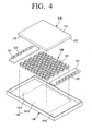
- FIG. 3 is a perspective view illustrating the bottom chassis, and components mounted to the bottom chassis, provided in the liquid crystal display apparatus of FIG. 1
- FIG. 4 is a perspective view illustrating dissembled components of FIG. 3 .
- the strength reinforcing member 160 is placed in a central portion of the bottom chassis 140. Therefore, the internal surface 141 of the bottom chassis 140 is divided into an occupied area 141a which is occupied by the strength reinforcing member 160 and a non-occupied area 141b which is not occupied by the strength reinforcing member 160.
- the occupied area 141a is expressed in virtual rectangular dotted lines, and a shape and size area of the occupied area 141a may change according to a shape and area of the strength reinforcing member 160.
- the non-occupied area 141b two light source PCBs 121 are mounted, and the strength reinforcing member 160 is provided therebetween.
- one light source PCB 121 is provided on each side of the strength reinforcing member 160.
- the strength reinforcing member 160 is attached to the bottom chassis 140 by, for example, an adhesive such as a hot melt adhesive. As illustrated in FIG. 4 , the strength reinforcing member 160 has a plurality of cells 161, wherein each cell has a shape of a hexagonal column. Therefore, the strength reinforcing member 160 has an overall shape of a honeycomb. However, this is only an example, and in other alternative exemplary embodiments, a shape of each cell 161 may be changed to have other various shapes, for example other columnar shapes, for example, a tetragonal column shape or a cylindrical shape etc.
- the strength reinforcing member 160 is made of aluminium, and may be advantageously made of aluminium with high strength. However, it is not limited thereto, and thus the strength reinforcing member 160 may be made of other metal materials or non-metal materials, such as, for example, plastic.
- the strength reinforcing member 160 having a shape of a honeycomb may be mounted to the bottom chassis 140, thereby significantly reinforcing of the bottom chassis 140 and improving the strength properties of the bottom chassis 140. Accordingly, the deformation of the bottom chassis 140 by weight, external force, or heat etc. may be minimized, so a good flatness of the bottom chassis 140 can be maintained. Thus, it is possible to prevent deterioration of the quality of images displayed by the liquid crystal panel 110 that would otherwise be caused by such deformation of the bottom chassis 140.
- the strength reinforcing member 160 does not increase the thickness of the bottom chassis 140 in order to achieve an improvement in the strength properties of the bottom chassis 140, and since the strength reinforcing member 160 is attached to the bottom chassis 140 relatively simply through an adhesive, it is possible to improve the strength properties of the bottom chassis 140 while maintaining a low manufacturing cost and high productivity.
- the liquid crystal display apparatus 100 is applied to a large size display apparatus, for example a television of 139.7 cm (55 inches) or more, it is possible to maintain a good flatness of the bottom chassis 140 by means of the aforementioned strength reinforcing member 160.
- the size area of the bottom chassis 140 becomes significantly large, and thus it is advantageous to prevent deformation of the bottom chassis 140 and maintain a good flatness thereof.
- the cover member 170 covers the strength reinforcing member 160 so that the strength reinforcing member 160 is not exposed. Accordingly, the cover member 170 includes an upper portion 171 which covers the upper side of the strength reinforcing member 160 and a side portion 172 which covers the border of the strength reinforcing member 160. For example, the side portion 172 may be formed through a bending process.
- the cover member 170 may be made of a same material as the strength reinforcing member 160. Therefore, the cover member 170 may be made of, for example, aluminium.
- the cover member 170 is attached to the strength reinforcing member 160, for example, by an adhesive such as hot melt.
- the cover member 170 Since the strength reinforcing member 160 is covered by the cover member 170, pollutants that may exist in the strength reinforcing member 160 and that may cause a deterioration in the performance of the liquid crystal display apparatus 100 may be prevented from entering the liquid crystal display apparatus 100. For example, particles generated during processing of or formation of the strength reinforcing member 160 may be examples of such a pollutant.
- the cover member 170 may also perform a function of supporting components such as the light guide plate 120 placed in its upper side.
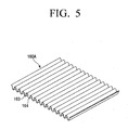
- FIG. 5 is a perspective view illustrating a strength reinforcing member provided in the liquid crystal display apparatus of FIG. 1 according to an alternative exemplary embodiment
- FIG. 6 is a perspective view illustrating a strength reinforcing member provided in the liquid crystal display apparatus of FIG. 1 according to another alternative exemplary embodiment.
- the alternative strength reinforcing member 160A is corrugated, also referred to as having an undulating or waved-shaped surface. More particularly, the strength reinforcing member 160A has a structure where convex portions 163 and concave portions 164 are repeated periodically.
- the convex portions 163 and concave portions 164 extend along a width direction or longitudinal direction of the strength reinforcing member 160A. That is, a concave portion 164 is placed between two convex portions 163, and a convex portion 163 is placed between two concave portions 163.
- another alternative strength reinforcing member 160B has a shape of an egg container, having a matrix of recessed portions or cells, divided by partitioning walls. More particularly, the strength reinforcing member 160B has a plurality of convex portions 165, corresponding to the partitioning walls, and a plurality of concave portions 166, corresponding to the recessed portions, which are repeated regularly in a two dimensional array, and a concave portion 166 is placed between four convex portions 165, and a convex portion 165 is placed between four concave portions 166.
- FIG.7 is a similar view to FIG. 2 , which illustrates a cross-sectional view of a liquid crystal display apparatus according to a second exemplary embodiment.
- the configuration of the liquid crystal display apparatus 100' illustrated in FIG.7 is similar to the configuration of the liquid crystal display apparatus 100 illustrated in the aforementioned FIG. 1 .
- the strength reinforcing member 160 is attached directly to the bottom chassis 140, whereas in the case of the liquid crystal display apparatus 100', there is a difference that the strength reinforcing member 160 is mounted to the bottom chassis 140 through an additional lower side cover member 175.
- the liquid crystal display apparatus 100' further includes a lower side cover member 175 in addition to the upper side cover member 170, and the strength reinforcing member 160 is surrounded by the upper side cover member 170 and the lower side cover member 175.
- the lower side cover member 175, strength reinforcing member 160, and upper side cover member 170 may be attached sequentially on the bottom chassis 140, but the lower side cover member 175, strength reinforcing member 160, and upper side cover member 170 may also be mutually and individually bonded to each other first to form one strength reinforcing unit 101, and then bonded to the bottom chassis 140 at once by use of an adhesive, such as an adhesive tape or other such bonding method.
- the formation of one strength reinforcing unit 101, prior to bonding to the bottom chassis 140 has an advantage of simplifying the manufacturing process of the liquid crystal display apparatus 100'.
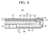
- FIG. 8 is a similar view to FIG. 2 , which illustrates a cross-sectional view of a liquid crystal display apparatus according to third exemplary embodiment.
- an alternative liquid crystal display apparatus 100A is similar to the configuration of the liquid crystal display apparatus 100 illustrated in the aforementioned FIG. 1 .
- the alternative liquid crystal display apparatus 100A is similar to the liquid crystal display apparatus 100 of FIG. 1 in that a strength reinforcing member 160 for strength reinforcement is mounted to the bottom chassis 140A.
- the difference of the liquid crystal display apparatus 100A from the aforementioned liquid crystal display apparatus 100 is that the liquid crystal display apparatus 100A further includes a heat sink 180 placed between a light source PCB 121 and the bottom chassis 140A.
- the heat sink 180 is made of a material, for example, aluminium, having a high thermal conductivity, to further effectively deliver the heat generated by the light sources 122 to the bottom chassis 140A.
- Such a heat sink 180 includes a body part 181 which supports the light source PCB 121 and a coupling part 182 substantially orthogonal to the body part 181.
- the coupling part 182 is fastened to the top chassis 130 by a fastener, thereby being directly coupled to the top chassis 130.
- the heat sink 180 may be alternatively directly coupled to the mid mold 150.
- FIG. 9 is a similar view to FIG. 2 , which illustrates however a cross-sectional view of a liquid crystal display apparatus not according to the present invention.
- another alternative liquid crystal display apparatus 100B is also similar to the aforementioned liquid crystal display apparatus 100 illustrated in FIG. 1 .
- the liquid crystal display apparatus 100B is similar to the liquid crystal display apparatus 100 of FIG. 1 in that a strength reinforcing member 160 for strength reinforcement is mounted to a bottom chassis 140B.
- the difference of the liquid crystal display apparatus 100B from the aforementioned liquid crystal display apparatus 100 is that the liquid crystal display apparatus 100B further includes a heat sink 190 placed at a rear side of the bottom chassis 140B.
- the heat sink 190 is made of a material, for example, aluminum, having a high thermal conductivity, to further effectively deliver the heat generated by the light sources 122 to the outside.
- Such a heat sink 190 includes a body part 191 and a coupling part 192.
- the body part 191 supports not only a light source PCB 121 but also the bottom chassis 140B. Since the light source PCB 121 is not supported by the bottom chassis 140B directly, compared to exemplary embodiments, the size (e.g., the width in the right to left direction in FIG. 1 , or the area, etc.) of the bottom chassis 140B may be reduced. For example, the width of the bottom chassis 140B may be reduced to be the same as the width of the cover member 170.
- the coupling part 192 is fastened to the top chassis 130 by a fastener (not illustrated) such as a screw, the heat sink 190 may be directly coupled to the top chassis 130. As an alternative, the heat sink 190 may be directly fastened to the mid mold 150.
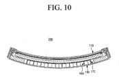
- FIG. 10 is a cross-sectional view illustrating a liquid crystal display apparatus according to a fourth exemplary embodiment
- FIG. 11 is an enlarged cross-sectional view of a right end portion of the liquid crystal display apparatus illustrated in FIG. 10 .
- the liquid crystal display apparatus 200 is a curved display apparatus, unlike the aforementioned liquid crystal display apparatuses.
- the detailed configuration of the liquid crystal panel 110, the backlight unit 120, the top chassis 130, the bottom chassis 140, the mid mold 150, and the strength reinforcing member 160 of the liquid crystal display apparatus 200 are provided in substantially the same manner as those of the aforementioned liquid crystal display apparatuses 100, but since the liquid crystal display apparatus 200 is a curved surface display with a curvature, the liquid crystal panel 110, the backlight unit 120, the top chassis 130, the bottom chassis 140, the mid mold 150, and the strength reinforcing member 160 of the liquid crystal display apparatus 200 are formed to conform to such a curvature.
- the bottom chassis 140 of the liquid crystal display apparatus 200 is also formed to conform to such a curvature. It is thus advantageous for the bottom chassis 140 to have good strength performance and properties so as to maintain the curvature.
- Various methods may be applied to manufacture the liquid crystal display apparatus 200 in a curved shape.
- a manufacturing method may be used where, after manufacturing a bottom chassis 140 of a curved surface shape, a top chassis 130 of a non-curved surface shape is assembled to the bottom chassis 140, thereby having other components such as the top chassis 130, etc. to conform to the curvature of the bottom chassis 140.
- the strength of the bottom chassis 140 is not sufficient, it may be difficult to maintain the curved surface shape of the liquid crystal display apparatus 200, and thus good strength performance of the bottom chassis 140 is advantageous.
- a strength reinforcing member 160 of a honeycomb shape is mounted to the internal surface 141 of the bottom chassis 140, for reinforcing the strength of the bottom chassis 140.
- the strength of the bottom chassis 140 where the strength reinforcing member 160 of a honeycomb shape is attached may be reinforced significantly, and accordingly, even when a weight, external force, or heat, etc. are applied to the liquid crystal display apparatus 200, the liquid crystal display apparatus 200 may maintain the initial curvature with stability. Therefore, it is possible to prevent the quality of the images provided by the liquid crystal display apparatus 200 from being deteriorated due to deformation of the bottom chassis 140 from the original manufactured curvature.
- the fourth exemplary embodiment was described as having a strength reinforcing member 160 having a honeycomb shape as the shape of the strength reinforcing member 160, but as aforementioned, a wave shape, or egg carton shape, etc. may also be applied as an alternative shape of the strength reinforcing member 160.
- a strength reinforcing member may be mounted to a bottom chassis, to significantly improve the strength of the bottom chassis, thereby minimizing deformation of the bottom chassis due to weight, external force, and heat, etc. Therefore, in a case where the present invention is applied to a flat panel display apparatus, it is possible to maintain a good flatness of the flat panel display apparatus, and in a case where the present invention is applied to the curved display apparatus, it is possible to maintain the initial curvature with stability. Consequently, it is possible to prevent deterioration, caused by excessive deformation of the bottom chassis, of the quality of the images that the display apparatus provides.
- the liquid crystal display apparatus may be applied to such a large size display apparatus particularly advantageously.
Landscapes
- Physics & Mathematics (AREA)
- Nonlinear Science (AREA)
- General Physics & Mathematics (AREA)
- Optics & Photonics (AREA)
- Mathematical Physics (AREA)
- Chemical & Material Sciences (AREA)
- Crystallography & Structural Chemistry (AREA)
- Liquid Crystal (AREA)
- Devices For Indicating Variable Information By Combining Individual Elements (AREA)
Claims (12)
- Appareil d'affichage à cristaux liquides (100) comprenant :un panneau à cristaux liquides (110) configuré pour afficher une image ;une unité de rétroéclairage (120) configurée pour s'allumer afin d'afficher l'image sur le panneau à cristaux liquides ;un châssis supérieur (130) et un châssis inférieur (140) qui enchâssent le panneau à cristaux liquides et l'unité de rétroéclairage dans un même module ; etun élément de renforcement de résistance (160) qui est monté sur une surface interne (141) du châssis inférieur pour renforcer la résistance du châssis inférieur ;caractérisé en ce que l'unité de rétroéclairage comprend au moins une plaquette à circuit imprimé, PCI, de sources de lumière (121) sur laquelle est montée une pluralité de sources de lumière (122), etdans lequel l'élément de renforcement de résistance occupe une zone partielle (141a) de la surface interne du châssis inférieur, et l'au moins une PCI de sources de lumière est montée sur une autre zone (141b) de la surface interne du châssis inférieur qui n'est pas occupée par l'élément de renforcement de résistance.
- Appareil d'affichage à cristaux liquides selon la revendication 1, dans lequel l'élément de renforcement de résistance contient une matrice bidirectionnelle de cellules (161) bornées par des parois de séparation.
- Appareil d'affichage à cristaux liquides selon la revendication 2, dans lequel chaque cellule de l'élément de renforcement de résistance a une forme de colonne hexagonale, si bien que l'élément de renforcement de résistance a la forme d'un nid d'abeille.
- Appareil d'affichage à cristaux liquides selon la revendication 2, dans lequel l'élément de renforcement de résistance (160B) a une forme de boîte à oeufs.
- Appareil d'affichage à cristaux liquides selon la revendication 4, dans lequel l'élément de renforcement de résistance (160B) comprend une pluralité de parties convexes (165) et une pluralité de parties concaves (166), et
dans lequel une partie concave est placée entre quatre parties convexes et une partie convexe est placée entre quatre parties concaves. - Appareil d'affichage à cristaux liquides selon la revendication 1, dans lequel l'élément de renforcement de résistance (160A) est ondulé.
- Appareil d'affichage à cristaux liquides selon l'une quelconque des revendications précédentes, comprenant en outre un élément de couverture (170) qui couvre l'élément de renforcement de résistance.
- Appareil d'affichage à cristaux liquides (100A) selon l'une quelconque des revendications précédentes, dans lequel un dissipateur thermique (180) destiné à transmettre la chaleur générée par les sources de lumière au châssis inférieur (140A) est placé entre la PCI de sources de lumière et le châssis inférieur.
- Appareil d'affichage à cristaux liquides selon la revendication 8, dans lequel le dissipateur thermique est fixé directement au châssis supérieur.
- Appareil d'affichage à cristaux liquides selon l'une quelconque des revendications précédentes, dans lequel l'élément de renforcement de résistance est réalisé en aluminium.
- Appareil d'affichage incurvé fourni comme appareil d'affichage à cristaux liquides selon l'une quelconque des revendications 1 à 10.
- Appareil d'affichage à cristaux liquides selon l'une quelconque des revendications précédentes, l'appareil d'affichage à cristaux liquides étant appliqué à une télévision grand format de 139,7 cm (55 pouces) ou plus.
Applications Claiming Priority (2)
| Application Number | Priority Date | Filing Date | Title |
|---|---|---|---|
| KR20120056184 | 2012-05-25 | ||
| KR1020120127641A KR102013932B1 (ko) | 2012-05-25 | 2012-11-12 | 액정 디스플레이 장치 |
Publications (2)
| Publication Number | Publication Date |
|---|---|
| EP2667247A1 EP2667247A1 (fr) | 2013-11-27 |
| EP2667247B1 true EP2667247B1 (fr) | 2014-12-03 |
Family
ID=48463856
Family Applications (1)
| Application Number | Title | Priority Date | Filing Date |
|---|---|---|---|
| EP13168931.7A Active EP2667247B1 (fr) | 2012-05-25 | 2013-05-23 | Appareil d'affichage à cristaux liquides |
Country Status (4)
| Country | Link |
|---|---|
| US (1) | US9310647B2 (fr) |
| EP (1) | EP2667247B1 (fr) |
| JP (1) | JP6154195B2 (fr) |
| WO (1) | WO2013176399A1 (fr) |
Families Citing this family (18)
| Publication number | Priority date | Publication date | Assignee | Title |
|---|---|---|---|---|
| KR20140021788A (ko) * | 2012-08-10 | 2014-02-20 | 삼성전자주식회사 | 프로젝션 장치 |
| KR102081112B1 (ko) | 2013-07-31 | 2020-02-25 | 엘지디스플레이 주식회사 | 곡면 디스플레이 장치 및 그의 곡률 제어 방법 |
| KR102148718B1 (ko) | 2013-12-18 | 2020-08-27 | 삼성전자주식회사 | 디스플레이 기기 |
| KR102171307B1 (ko) * | 2013-12-19 | 2020-10-28 | 삼성전자주식회사 | 입체 영상 디스플레이 장치 및 그 제조 방법 |
| KR20150095024A (ko) * | 2014-02-12 | 2015-08-20 | 삼성디스플레이 주식회사 | 표시 장치 |
| KR102241557B1 (ko) | 2014-09-22 | 2021-04-19 | 삼성디스플레이 주식회사 | 표시 장치 |
| KR20160035132A (ko) | 2014-09-22 | 2016-03-31 | 삼성디스플레이 주식회사 | 표시 장치 |
| JP2016103396A (ja) | 2014-11-28 | 2016-06-02 | 三菱電機株式会社 | バックライトおよび表示装置 |
| WO2016136218A1 (fr) * | 2015-02-23 | 2016-09-01 | パナソニックIpマネジメント株式会社 | Dispositif d'affichage et plaque arrière utilisée dans ledit dispositif d'affichage |
| JP6587506B2 (ja) * | 2015-11-04 | 2019-10-09 | 正寿 戸田 | 照明装置 |
| KR102600981B1 (ko) | 2016-04-29 | 2023-11-13 | 삼성전자주식회사 | 디스플레이 장치 |
| JP7012719B2 (ja) * | 2016-11-14 | 2022-02-14 | シーメンス・ヘルスケア・ダイアグノスティックス・インコーポレーテッド | パターン照明を用いて試料を特徴付ける方法及び装置 |
| US10481320B2 (en) * | 2017-10-13 | 2019-11-19 | HKC Corporation Limited | Clamping method and display device |
| KR102612785B1 (ko) | 2018-12-20 | 2023-12-13 | 엘지전자 주식회사 | 디스플레이 디바이스 |
| JP7323251B2 (ja) * | 2019-07-24 | 2023-08-08 | スタンレー電気株式会社 | 発光装置の製造方法、及び、発光装置 |
| WO2021141144A1 (fr) * | 2020-01-06 | 2021-07-15 | 엘지전자 주식회사 | Dispositif d'affichage |
| WO2023080270A1 (fr) * | 2021-11-04 | 2023-05-11 | 엘지전자 주식회사 | Dispositif d'affichage |
| KR20240102590A (ko) * | 2022-12-26 | 2024-07-03 | 엘지디스플레이 주식회사 | 표시 장치 |
Family Cites Families (16)
| Publication number | Priority date | Publication date | Assignee | Title |
|---|---|---|---|---|
| DE20001729U1 (de) | 2000-02-01 | 2001-06-21 | R+S Technik GmbH, 63073 Offenbach | Plattenförmiges Element und Vorrichtung zu seiner Herstellung |
| KR100589313B1 (ko) * | 2003-09-24 | 2006-06-14 | 삼성에스디아이 주식회사 | 플라즈마 디스플레이 장치 |
| US8142049B2 (en) * | 2007-03-09 | 2012-03-27 | Sharp Kabushiki Kaisha | Lighting device for display device and display device |
| JP2008276035A (ja) * | 2007-05-02 | 2008-11-13 | Seiko Epson Corp | 電子機器、表示装置および保護カバー |
| JP4722082B2 (ja) * | 2007-05-17 | 2011-07-13 | シャープ株式会社 | バックライト装置及び表示装置 |
| KR100872864B1 (ko) * | 2007-06-29 | 2008-12-10 | 중앙대학교 산학협력단 | 엘엔지 저장탱크를 위한 단열체 및 그의 제조방법 |
| JP4909866B2 (ja) * | 2007-10-10 | 2012-04-04 | 富士フイルム株式会社 | 面状照明装置 |
| JP2009244668A (ja) * | 2008-03-31 | 2009-10-22 | Idemitsu Kosan Co Ltd | 表示装置用の筐体およびこれを用いた表示装置 |
| JP2010002487A (ja) | 2008-06-18 | 2010-01-07 | Hitachi Displays Ltd | 液晶表示装置 |
| KR101255833B1 (ko) * | 2009-07-09 | 2013-04-16 | 엘지디스플레이 주식회사 | 액정표시장치 |
| WO2011024254A1 (fr) | 2009-08-25 | 2011-03-03 | 富士通株式会社 | Structure de boîtier, dispositif électronique et son procédé de fabrication |
| KR101698754B1 (ko) | 2009-10-19 | 2017-01-24 | 삼성디스플레이 주식회사 | 백라이트 어셈블리 및 그를 포함하는 액정 표시 장치 |
| KR101024692B1 (ko) * | 2010-06-07 | 2011-03-25 | 남영정밀 주식회사 | 건축용 실내 바닥재 및 그 제조방법 |
| JP4875188B2 (ja) | 2010-06-18 | 2012-02-15 | 株式会社東芝 | テレビジョン装置および電子機器 |
| KR101687783B1 (ko) * | 2010-08-24 | 2016-12-16 | 엘지디스플레이 주식회사 | 액정표시장치 |
| KR101945890B1 (ko) | 2011-12-30 | 2019-02-12 | 삼성전자주식회사 | 디스플레이 장치 |
-
2013
- 2013-04-08 WO PCT/KR2013/002918 patent/WO2013176399A1/fr not_active Ceased
- 2013-04-26 US US13/871,623 patent/US9310647B2/en active Active
- 2013-05-22 JP JP2013107616A patent/JP6154195B2/ja active Active
- 2013-05-23 EP EP13168931.7A patent/EP2667247B1/fr active Active
Also Published As
| Publication number | Publication date |
|---|---|
| JP6154195B2 (ja) | 2017-06-28 |
| WO2013176399A1 (fr) | 2013-11-28 |
| US9310647B2 (en) | 2016-04-12 |
| CN103424898A (zh) | 2013-12-04 |
| US20130314638A1 (en) | 2013-11-28 |
| JP2013246442A (ja) | 2013-12-09 |
| EP2667247A1 (fr) | 2013-11-27 |
Similar Documents
| Publication | Publication Date | Title |
|---|---|---|
| EP2667247B1 (fr) | Appareil d'affichage à cristaux liquides | |
| US9338905B2 (en) | Curved display apparatus | |
| EP2352058B1 (fr) | Dispositif d'affichage à cristaux liquides comprenant une pluralité de modules d'affichage à cristaux liquides | |
| US9826654B2 (en) | Display | |
| KR101319543B1 (ko) | 곡면 디스플레이 장치 및 이를 포함하는 멀티 디스플레이 장치 | |
| US9563078B2 (en) | Frame for display device and display device having the same | |
| KR102013932B1 (ko) | 액정 디스플레이 장치 | |
| EP2626737B1 (fr) | Élément de support pour unité de rétroéclairage, unité de rétroéclairage et appareil d'affichage d'image équipé de celle-ci | |
| EP3121645B1 (fr) | Dispositif d'affichage à cristaux liquides | |
| US20150212261A1 (en) | Lighting apparatus, display apparatus, and television receiver | |
| US9507079B2 (en) | Display apparatus | |
| US9389460B2 (en) | Display device including supporting member having corner reflective surface | |
| US9470379B2 (en) | Display apparatus | |
| US20130107156A1 (en) | Backplane, Back Light Module and Liquid Crystal Display Device | |
| US20190141281A1 (en) | Display device | |
| US9319621B2 (en) | Display apparatus and television receiver | |
| US20100045890A1 (en) | Backlight unit and liquid crystal display | |
| CN101441350B (zh) | 液晶显示器 | |
| US20120194761A1 (en) | Liquid crystal module and display device | |
| US9609774B2 (en) | Display module and display apparatus having the same | |
| US8870440B2 (en) | Back light module and liquid crystal display device having the same | |
| CN103424898B (zh) | 液晶显示设备 | |
| KR20200136536A (ko) | 게임기의 이중 표시장치에 대한 결합 어셈블리 | |
| KR20070071299A (ko) | 액정표시장치 |
Legal Events
| Date | Code | Title | Description |
|---|---|---|---|
| PUAI | Public reference made under article 153(3) epc to a published international application that has entered the european phase |
Free format text: ORIGINAL CODE: 0009012 |
|
| AK | Designated contracting states |
Kind code of ref document: A1 Designated state(s): AL AT BE BG CH CY CZ DE DK EE ES FI FR GB GR HR HU IE IS IT LI LT LU LV MC MK MT NL NO PL PT RO RS SE SI SK SM TR |
|
| AX | Request for extension of the european patent |
Extension state: BA ME |
|
| 17P | Request for examination filed |
Effective date: 20140327 |
|
| RBV | Designated contracting states (corrected) |
Designated state(s): AL AT BE BG CH CY CZ DE DK EE ES FI FR GB GR HR HU IE IS IT LI LT LU LV MC MK MT NL NO PL PT RO RS SE SI SK SM TR |
|
| RIC1 | Information provided on ipc code assigned before grant |
Ipc: F21V 8/00 20060101ALI20140505BHEP Ipc: G02F 1/1333 20060101AFI20140505BHEP |
|
| GRAP | Despatch of communication of intention to grant a patent |
Free format text: ORIGINAL CODE: EPIDOSNIGR1 |
|
| INTG | Intention to grant announced |
Effective date: 20140616 |
|
| GRAS | Grant fee paid |
Free format text: ORIGINAL CODE: EPIDOSNIGR3 |
|
| GRAP | Despatch of communication of intention to grant a patent |
Free format text: ORIGINAL CODE: EPIDOSNIGR1 |
|
| GRAA | (expected) grant |
Free format text: ORIGINAL CODE: 0009210 |
|
| INTG | Intention to grant announced |
Effective date: 20141015 |
|
| AK | Designated contracting states |
Kind code of ref document: B1 Designated state(s): AL AT BE BG CH CY CZ DE DK EE ES FI FR GB GR HR HU IE IS IT LI LT LU LV MC MK MT NL NO PL PT RO RS SE SI SK SM TR |
|
| REG | Reference to a national code |
Ref country code: GB Ref legal event code: FG4D |
|
| REG | Reference to a national code |
Ref country code: AT Ref legal event code: REF Ref document number: 699696 Country of ref document: AT Kind code of ref document: T Effective date: 20141215 Ref country code: CH Ref legal event code: EP |
|
| REG | Reference to a national code |
Ref country code: IE Ref legal event code: FG4D |
|
| REG | Reference to a national code |
Ref country code: DE Ref legal event code: R096 Ref document number: 602013000558 Country of ref document: DE Effective date: 20150115 |
|
| REG | Reference to a national code |
Ref country code: NL Ref legal event code: T3 |
|
| REG | Reference to a national code |
Ref country code: AT Ref legal event code: MK05 Ref document number: 699696 Country of ref document: AT Kind code of ref document: T Effective date: 20141203 |
|
| PG25 | Lapsed in a contracting state [announced via postgrant information from national office to epo] |
Ref country code: FI Free format text: LAPSE BECAUSE OF FAILURE TO SUBMIT A TRANSLATION OF THE DESCRIPTION OR TO PAY THE FEE WITHIN THE PRESCRIBED TIME-LIMIT Effective date: 20141203 Ref country code: ES Free format text: LAPSE BECAUSE OF FAILURE TO SUBMIT A TRANSLATION OF THE DESCRIPTION OR TO PAY THE FEE WITHIN THE PRESCRIBED TIME-LIMIT Effective date: 20141203 Ref country code: LT Free format text: LAPSE BECAUSE OF FAILURE TO SUBMIT A TRANSLATION OF THE DESCRIPTION OR TO PAY THE FEE WITHIN THE PRESCRIBED TIME-LIMIT Effective date: 20141203 Ref country code: NO Free format text: LAPSE BECAUSE OF FAILURE TO SUBMIT A TRANSLATION OF THE DESCRIPTION OR TO PAY THE FEE WITHIN THE PRESCRIBED TIME-LIMIT Effective date: 20150303 |
|
| REG | Reference to a national code |
Ref country code: LT Ref legal event code: MG4D |
|
| PG25 | Lapsed in a contracting state [announced via postgrant information from national office to epo] |
Ref country code: SE Free format text: LAPSE BECAUSE OF FAILURE TO SUBMIT A TRANSLATION OF THE DESCRIPTION OR TO PAY THE FEE WITHIN THE PRESCRIBED TIME-LIMIT Effective date: 20141203 Ref country code: GR Free format text: LAPSE BECAUSE OF FAILURE TO SUBMIT A TRANSLATION OF THE DESCRIPTION OR TO PAY THE FEE WITHIN THE PRESCRIBED TIME-LIMIT Effective date: 20150304 Ref country code: CY Free format text: LAPSE BECAUSE OF FAILURE TO SUBMIT A TRANSLATION OF THE DESCRIPTION OR TO PAY THE FEE WITHIN THE PRESCRIBED TIME-LIMIT Effective date: 20141203 Ref country code: RS Free format text: LAPSE BECAUSE OF FAILURE TO SUBMIT A TRANSLATION OF THE DESCRIPTION OR TO PAY THE FEE WITHIN THE PRESCRIBED TIME-LIMIT Effective date: 20141203 Ref country code: LV Free format text: LAPSE BECAUSE OF FAILURE TO SUBMIT A TRANSLATION OF THE DESCRIPTION OR TO PAY THE FEE WITHIN THE PRESCRIBED TIME-LIMIT Effective date: 20141203 Ref country code: HR Free format text: LAPSE BECAUSE OF FAILURE TO SUBMIT A TRANSLATION OF THE DESCRIPTION OR TO PAY THE FEE WITHIN THE PRESCRIBED TIME-LIMIT Effective date: 20141203 Ref country code: AT Free format text: LAPSE BECAUSE OF FAILURE TO SUBMIT A TRANSLATION OF THE DESCRIPTION OR TO PAY THE FEE WITHIN THE PRESCRIBED TIME-LIMIT Effective date: 20141203 |
|
| PG25 | Lapsed in a contracting state [announced via postgrant information from national office to epo] |
Ref country code: RO Free format text: LAPSE BECAUSE OF FAILURE TO SUBMIT A TRANSLATION OF THE DESCRIPTION OR TO PAY THE FEE WITHIN THE PRESCRIBED TIME-LIMIT Effective date: 20141203 Ref country code: PT Free format text: LAPSE BECAUSE OF FAILURE TO SUBMIT A TRANSLATION OF THE DESCRIPTION OR TO PAY THE FEE WITHIN THE PRESCRIBED TIME-LIMIT Effective date: 20150403 Ref country code: EE Free format text: LAPSE BECAUSE OF FAILURE TO SUBMIT A TRANSLATION OF THE DESCRIPTION OR TO PAY THE FEE WITHIN THE PRESCRIBED TIME-LIMIT Effective date: 20141203 Ref country code: SK Free format text: LAPSE BECAUSE OF FAILURE TO SUBMIT A TRANSLATION OF THE DESCRIPTION OR TO PAY THE FEE WITHIN THE PRESCRIBED TIME-LIMIT Effective date: 20141203 Ref country code: CZ Free format text: LAPSE BECAUSE OF FAILURE TO SUBMIT A TRANSLATION OF THE DESCRIPTION OR TO PAY THE FEE WITHIN THE PRESCRIBED TIME-LIMIT Effective date: 20141203 |
|
| PG25 | Lapsed in a contracting state [announced via postgrant information from national office to epo] |
Ref country code: PL Free format text: LAPSE BECAUSE OF FAILURE TO SUBMIT A TRANSLATION OF THE DESCRIPTION OR TO PAY THE FEE WITHIN THE PRESCRIBED TIME-LIMIT Effective date: 20141203 Ref country code: IS Free format text: LAPSE BECAUSE OF FAILURE TO SUBMIT A TRANSLATION OF THE DESCRIPTION OR TO PAY THE FEE WITHIN THE PRESCRIBED TIME-LIMIT Effective date: 20150403 |
|
| REG | Reference to a national code |
Ref country code: DE Ref legal event code: R097 Ref document number: 602013000558 Country of ref document: DE |
|
| PLBE | No opposition filed within time limit |
Free format text: ORIGINAL CODE: 0009261 |
|
| STAA | Information on the status of an ep patent application or granted ep patent |
Free format text: STATUS: NO OPPOSITION FILED WITHIN TIME LIMIT |
|
| PG25 | Lapsed in a contracting state [announced via postgrant information from national office to epo] |
Ref country code: DK Free format text: LAPSE BECAUSE OF FAILURE TO SUBMIT A TRANSLATION OF THE DESCRIPTION OR TO PAY THE FEE WITHIN THE PRESCRIBED TIME-LIMIT Effective date: 20141203 |
|
| 26N | No opposition filed |
Effective date: 20150904 |
|
| PG25 | Lapsed in a contracting state [announced via postgrant information from national office to epo] |
Ref country code: IT Free format text: LAPSE BECAUSE OF FAILURE TO SUBMIT A TRANSLATION OF THE DESCRIPTION OR TO PAY THE FEE WITHIN THE PRESCRIBED TIME-LIMIT Effective date: 20141203 |
|
| PG25 | Lapsed in a contracting state [announced via postgrant information from national office to epo] |
Ref country code: LU Free format text: LAPSE BECAUSE OF FAILURE TO SUBMIT A TRANSLATION OF THE DESCRIPTION OR TO PAY THE FEE WITHIN THE PRESCRIBED TIME-LIMIT Effective date: 20150523 Ref country code: MC Free format text: LAPSE BECAUSE OF FAILURE TO SUBMIT A TRANSLATION OF THE DESCRIPTION OR TO PAY THE FEE WITHIN THE PRESCRIBED TIME-LIMIT Effective date: 20141203 |
|
| REG | Reference to a national code |
Ref country code: IE Ref legal event code: MM4A |
|
| PG25 | Lapsed in a contracting state [announced via postgrant information from national office to epo] |
Ref country code: SI Free format text: LAPSE BECAUSE OF FAILURE TO SUBMIT A TRANSLATION OF THE DESCRIPTION OR TO PAY THE FEE WITHIN THE PRESCRIBED TIME-LIMIT Effective date: 20141203 |
|
| PG25 | Lapsed in a contracting state [announced via postgrant information from national office to epo] |
Ref country code: IE Free format text: LAPSE BECAUSE OF NON-PAYMENT OF DUE FEES Effective date: 20150523 |
|
| REG | Reference to a national code |
Ref country code: FR Ref legal event code: PLFP Year of fee payment: 4 |
|
| PG25 | Lapsed in a contracting state [announced via postgrant information from national office to epo] |
Ref country code: BE Free format text: LAPSE BECAUSE OF FAILURE TO SUBMIT A TRANSLATION OF THE DESCRIPTION OR TO PAY THE FEE WITHIN THE PRESCRIBED TIME-LIMIT Effective date: 20141203 |
|
| PG25 | Lapsed in a contracting state [announced via postgrant information from national office to epo] |
Ref country code: MT Free format text: LAPSE BECAUSE OF FAILURE TO SUBMIT A TRANSLATION OF THE DESCRIPTION OR TO PAY THE FEE WITHIN THE PRESCRIBED TIME-LIMIT Effective date: 20141203 |
|
| REG | Reference to a national code |
Ref country code: CH Ref legal event code: PL |
|
| PG25 | Lapsed in a contracting state [announced via postgrant information from national office to epo] |
Ref country code: CH Free format text: LAPSE BECAUSE OF NON-PAYMENT OF DUE FEES Effective date: 20160531 Ref country code: LI Free format text: LAPSE BECAUSE OF NON-PAYMENT OF DUE FEES Effective date: 20160531 |
|
| REG | Reference to a national code |
Ref country code: FR Ref legal event code: PLFP Year of fee payment: 5 |
|
| PG25 | Lapsed in a contracting state [announced via postgrant information from national office to epo] |
Ref country code: HU Free format text: LAPSE BECAUSE OF FAILURE TO SUBMIT A TRANSLATION OF THE DESCRIPTION OR TO PAY THE FEE WITHIN THE PRESCRIBED TIME-LIMIT; INVALID AB INITIO Effective date: 20130523 Ref country code: BG Free format text: LAPSE BECAUSE OF FAILURE TO SUBMIT A TRANSLATION OF THE DESCRIPTION OR TO PAY THE FEE WITHIN THE PRESCRIBED TIME-LIMIT Effective date: 20141203 |
|
| PG25 | Lapsed in a contracting state [announced via postgrant information from national office to epo] |
Ref country code: TR Free format text: LAPSE BECAUSE OF FAILURE TO SUBMIT A TRANSLATION OF THE DESCRIPTION OR TO PAY THE FEE WITHIN THE PRESCRIBED TIME-LIMIT Effective date: 20141203 |
|
| REG | Reference to a national code |
Ref country code: FR Ref legal event code: PLFP Year of fee payment: 6 |
|
| PG25 | Lapsed in a contracting state [announced via postgrant information from national office to epo] |
Ref country code: SM Free format text: LAPSE BECAUSE OF FAILURE TO SUBMIT A TRANSLATION OF THE DESCRIPTION OR TO PAY THE FEE WITHIN THE PRESCRIBED TIME-LIMIT Effective date: 20141203 |
|
| PG25 | Lapsed in a contracting state [announced via postgrant information from national office to epo] |
Ref country code: MK Free format text: LAPSE BECAUSE OF FAILURE TO SUBMIT A TRANSLATION OF THE DESCRIPTION OR TO PAY THE FEE WITHIN THE PRESCRIBED TIME-LIMIT Effective date: 20141203 |
|
| PG25 | Lapsed in a contracting state [announced via postgrant information from national office to epo] |
Ref country code: AL Free format text: LAPSE BECAUSE OF FAILURE TO SUBMIT A TRANSLATION OF THE DESCRIPTION OR TO PAY THE FEE WITHIN THE PRESCRIBED TIME-LIMIT Effective date: 20141203 |
|
| PGFP | Annual fee paid to national office [announced via postgrant information from national office to epo] |
Ref country code: NL Payment date: 20250422 Year of fee payment: 13 |
|
| PGFP | Annual fee paid to national office [announced via postgrant information from national office to epo] |
Ref country code: DE Payment date: 20250422 Year of fee payment: 13 |
|
| PGFP | Annual fee paid to national office [announced via postgrant information from national office to epo] |
Ref country code: FR Payment date: 20250422 Year of fee payment: 13 |
|
| PGFP | Annual fee paid to national office [announced via postgrant information from national office to epo] |
Ref country code: GB Payment date: 20260324 Year of fee payment: 14 |