EP2667376B1 - Gate-elektroden-treiberschaltung, gate-elektroden-ansteuerverfahren und flüssigkristallanzeigevorrichtung - Google Patents
Gate-elektroden-treiberschaltung, gate-elektroden-ansteuerverfahren und flüssigkristallanzeigevorrichtung Download PDFInfo
- Publication number
- EP2667376B1 EP2667376B1 EP12842680.6A EP12842680A EP2667376B1 EP 2667376 B1 EP2667376 B1 EP 2667376B1 EP 12842680 A EP12842680 A EP 12842680A EP 2667376 B1 EP2667376 B1 EP 2667376B1
- Authority
- EP
- European Patent Office
- Prior art keywords
- switching device
- unit
- terminal
- tft switching
- pull
- Prior art date
- Legal status (The legal status is an assumption and is not a legal conclusion. Google has not performed a legal analysis and makes no representation as to the accuracy of the status listed.)
- Active
Links
Images


Classifications
-
- G—PHYSICS
- G09—EDUCATION; CRYPTOGRAPHY; DISPLAY; ADVERTISING; SEALS
- G09G—ARRANGEMENTS OR CIRCUITS FOR CONTROL OF INDICATING DEVICES USING STATIC MEANS TO PRESENT VARIABLE INFORMATION
- G09G3/00—Control arrangements or circuits, of interest only in connection with visual indicators other than cathode-ray tubes
- G09G3/20—Control arrangements or circuits, of interest only in connection with visual indicators other than cathode-ray tubes for presentation of an assembly of a number of characters, e.g. a page, by composing the assembly by combination of individual elements arranged in a matrix no fixed position being assigned to or needed to be assigned to the individual characters or partial characters
- G09G3/34—Control arrangements or circuits, of interest only in connection with visual indicators other than cathode-ray tubes for presentation of an assembly of a number of characters, e.g. a page, by composing the assembly by combination of individual elements arranged in a matrix no fixed position being assigned to or needed to be assigned to the individual characters or partial characters by control of light from an independent source
- G09G3/36—Control arrangements or circuits, of interest only in connection with visual indicators other than cathode-ray tubes for presentation of an assembly of a number of characters, e.g. a page, by composing the assembly by combination of individual elements arranged in a matrix no fixed position being assigned to or needed to be assigned to the individual characters or partial characters by control of light from an independent source using liquid crystals
- G09G3/3611—Control of matrices with row and column drivers
-
- G—PHYSICS
- G09—EDUCATION; CRYPTOGRAPHY; DISPLAY; ADVERTISING; SEALS
- G09G—ARRANGEMENTS OR CIRCUITS FOR CONTROL OF INDICATING DEVICES USING STATIC MEANS TO PRESENT VARIABLE INFORMATION
- G09G3/00—Control arrangements or circuits, of interest only in connection with visual indicators other than cathode-ray tubes
- G09G3/20—Control arrangements or circuits, of interest only in connection with visual indicators other than cathode-ray tubes for presentation of an assembly of a number of characters, e.g. a page, by composing the assembly by combination of individual elements arranged in a matrix no fixed position being assigned to or needed to be assigned to the individual characters or partial characters
- G09G3/34—Control arrangements or circuits, of interest only in connection with visual indicators other than cathode-ray tubes for presentation of an assembly of a number of characters, e.g. a page, by composing the assembly by combination of individual elements arranged in a matrix no fixed position being assigned to or needed to be assigned to the individual characters or partial characters by control of light from an independent source
- G09G3/36—Control arrangements or circuits, of interest only in connection with visual indicators other than cathode-ray tubes for presentation of an assembly of a number of characters, e.g. a page, by composing the assembly by combination of individual elements arranged in a matrix no fixed position being assigned to or needed to be assigned to the individual characters or partial characters by control of light from an independent source using liquid crystals
-
- G—PHYSICS
- G09—EDUCATION; CRYPTOGRAPHY; DISPLAY; ADVERTISING; SEALS
- G09G—ARRANGEMENTS OR CIRCUITS FOR CONTROL OF INDICATING DEVICES USING STATIC MEANS TO PRESENT VARIABLE INFORMATION
- G09G3/00—Control arrangements or circuits, of interest only in connection with visual indicators other than cathode-ray tubes
- G09G3/20—Control arrangements or circuits, of interest only in connection with visual indicators other than cathode-ray tubes for presentation of an assembly of a number of characters, e.g. a page, by composing the assembly by combination of individual elements arranged in a matrix no fixed position being assigned to or needed to be assigned to the individual characters or partial characters
- G09G3/34—Control arrangements or circuits, of interest only in connection with visual indicators other than cathode-ray tubes for presentation of an assembly of a number of characters, e.g. a page, by composing the assembly by combination of individual elements arranged in a matrix no fixed position being assigned to or needed to be assigned to the individual characters or partial characters by control of light from an independent source
- G09G3/36—Control arrangements or circuits, of interest only in connection with visual indicators other than cathode-ray tubes for presentation of an assembly of a number of characters, e.g. a page, by composing the assembly by combination of individual elements arranged in a matrix no fixed position being assigned to or needed to be assigned to the individual characters or partial characters by control of light from an independent source using liquid crystals
- G09G3/3611—Control of matrices with row and column drivers
- G09G3/3674—Details of drivers for scan electrodes
- G09G3/3677—Details of drivers for scan electrodes suitable for active matrices only
-
- G—PHYSICS
- G11—INFORMATION STORAGE
- G11C—STATIC STORES
- G11C19/00—Digital stores in which the information is moved stepwise, e.g. shift registers
- G11C19/28—Digital stores in which the information is moved stepwise, e.g. shift registers using semiconductor elements
-
- G—PHYSICS
- G09—EDUCATION; CRYPTOGRAPHY; DISPLAY; ADVERTISING; SEALS
- G09G—ARRANGEMENTS OR CIRCUITS FOR CONTROL OF INDICATING DEVICES USING STATIC MEANS TO PRESENT VARIABLE INFORMATION
- G09G2310/00—Command of the display device
- G09G2310/02—Addressing, scanning or driving the display screen or processing steps related thereto
- G09G2310/0264—Details of driving circuits
- G09G2310/0286—Details of a shift registers arranged for use in a driving circuit
-
- G—PHYSICS
- G09—EDUCATION; CRYPTOGRAPHY; DISPLAY; ADVERTISING; SEALS
- G09G—ARRANGEMENTS OR CIRCUITS FOR CONTROL OF INDICATING DEVICES USING STATIC MEANS TO PRESENT VARIABLE INFORMATION
- G09G2320/00—Control of display operating conditions
- G09G2320/02—Improving the quality of display appearance
- G09G2320/0223—Compensation for problems related to R-C delay and attenuation in electrodes of matrix panels, e.g. in gate electrodes or on-substrate video signal electrodes
-
- G—PHYSICS
- G09—EDUCATION; CRYPTOGRAPHY; DISPLAY; ADVERTISING; SEALS
- G09G—ARRANGEMENTS OR CIRCUITS FOR CONTROL OF INDICATING DEVICES USING STATIC MEANS TO PRESENT VARIABLE INFORMATION
- G09G2320/00—Control of display operating conditions
- G09G2320/04—Maintaining the quality of display appearance
- G09G2320/041—Temperature compensation
Definitions
- the present invention relates to the technical field of gate driving, and in particular relates to a gate driving circuit, a gate driving method and a liquid crystal display (LCD).
- a gate driving circuit a gate driving circuit
- a gate driving method a gate driving method
- LCD liquid crystal display
- the LCD is a commonly-used panel display, wherein the Thin Film Transistor Liquid Crystal Display (TFT-LCD) is the mainstream product in the current liquid crystal displays.
- TFT-LCD Thin Film Transistor Liquid Crystal Display
- the manufacturers have to reduce the cost of their products by using new techniques, so as to enhance the market competitiveness of the products.
- GOA Gate on Array
- GOA Gate on Array
- An existing gate driving circuit includes shift registers at a plurality of stages
- Figure 1 is a structure diagram of the shift register at each stage in the existing gate driving circuit.
- said shift register at each stage comprises a first TFT switching device M1, a second TFT switching device M2, a third TFT switching device M3, a fourth TFT switching device M4, a pull-down unit PD and a boost device C1; wherein a drain and a gate of M1 is connected to an input terminal (INPUT), and receives an output signal of the shift register at a previous stage; a drain of M2 is connected to a source of M1, a gate of M2 is connected to a reset terminal (RESET) and receives an output signal of the shift register at a next stage, and a source of M2 is connected to a low-voltage signal terminal (VSS) and receives a low-voltage signal; a drain of M3 is connected to
- the operational principle of the aforementioned gate driving circuit is: when an input signal at INPUT is at a high level, M1 is turned on, and a node PU is charged; when a clock signal at the clock signal terminal is at the high level, M3 is turned on, the pulse of the clock signal is outputted at OUTPUT, and at the same time the node PU is further pulled up due to bootstrapping of C1; thereafter M2 and M4 are turned on by a reset signal at RESET, so as to discharge the node PU and OUTPUT.
- the circuit devices of the pull-down unit PD are controlled by the clock signal to discharge the node PU and OUTPUT, ensuring that there will be no noise occurring in the line corresponding to the shift register at the present stage during the non-operating time, the specific timing sequence of respective signals being as shown in Figure 2 .
- the shift register shown in Figure 1 is applied, at the instant of TFT being turned off, the signal at OUTPUT jumps from the high level to a low level, and the voltage jump of the pixel is large, thus affecting the picture quality of LCD.
- US 2008/036725 A1 , US 2004/189585 A1 , and US 2012/044132 A1 respectively discloses a gate driver, in which at the instant of the signal at an output terminal jumping to a low level, the signal at the output terminal directly jumps from the high level to the low level, and the voltage jump of the pixel is very large, thus affecting the picture quality of LCD.
- MLG multi-level gate
- ⁇ -Si process is adopted in the existing gate driving circuit.
- a solution of adding a temperature compensation circuit outside of the gate driving circuit is usually adopted, and particularly a thermo-sensitive device can be connected in parallel with the feedback circuit generating the gate high level Vgh to cause Vgh to rise with the temperature falling down.
- Vgh may rise to more than 30V, while DC/DC IC cannot withstand such a high voltage, and in this case the function of MLG will be deactivated. Once the function of MLG is deactivated, there will be a large voltage jump at the instant of TFT being turned off, thus affecting the picture quality of TFT panel.
- the main object of the present invention is to provide a gate driving circuit, a gate driving method and a display that can realize a gate driving circuit having a MLG function.
- an embodiment of the present disclosure provides a gate driving circuit, including a plurality of shift registers at a plurality of stages, wherein the shift register at each stage includes a pull-up driving unit, a pull-up unit, a reset unit and a pull-down unit, said shift register further including: a supplementary unit; wherein, said pull-up unit is used for making a clock signal at a first clock terminal an output signal of the shift register at the present stage when being turned on during a phase in which an input node of the pull-up unit is at a high level, the clock signal at the first clock terminal is at its high level and a clock signal at a second clock terminal is at a low level; said supplementary unit, connected to said pull-up unit, is used for making the clock signal at the second clock terminal the output signal of the shift register at the present stage when being turned on during another phase immediately after said phase in which the input node (PU) of the pull-up unit keeps at the high level, the clock signal at the first clock terminal (CLK1) jumps into
- said pull-up driving unit connected to the input node of the pull-up unit, is used for controlling ON and OFF of the pull-up unit.
- said pull-up driving unit comprises a first TFT switching device and a second TFT switching device; wherein, a drain and a gate of the first TFT switching device are connected to an output terminal of the shift register at a previous stage; a drain of said second TFT switching device is connected to the source of said first TFT switching device, a gate of said second TFT switching device is connected to an output terminal of the shift register at a next stage, and a source of said second TFT switching device is connected to a low level.
- said pull-up unit includes a third TFT switching device and a boost device; Wherein, a drain of said third TFT switching device is connected to the first clock terminal, a gate of said third TFT switching device is connected to the source of said first TFT switching device, and a source of said third TFT switching device is an output terminal of the shift register at the present stage; the boost device has a first terminal respectively connected to the source of said first TFT switching device and the gate of said third TFT switching device and a second terminal connected to the source of said third TFT switching device.
- said reset unit includes a fourth TFT switching device; a drain of said fourth TFT switching device is connected to the source of the third TFT switching device, a gate of said fourth TFT switching device is connected to the output terminal of the shift register at the next stage, and a source of said fourth TFT switching device is connected to the low level.
- said supplementary unit includes a fifth TFT switching device and a sixth TFT switching device; wherein, a drain and a gate of the fifth TFT switching device are connected to the second clock terminal, a drain of the sixth TFT switching device is connected to the source of the fifth TFT switching device, a gate of the sixth TFT switching device is connected to the source of the first TFT switching device of said pull-up driving unit, and a source of the sixth TFT switching device is connected to the output terminal of said pull-up unit and meanwhile serves as the output terminal of the shift register at the present stage.
- said fifth switching device and said sixth TFT switching device are metal-oxide-semiconductor field effect transistors.
- the clock signal at said second clock terminal jumps into its high level at the instant of the clock signal at the first clock terminal becoming the low level.
- An embodiment of the invention provides a liquid crystal display comprising the gate driving circuit as described above.
- the high level of the clock signal at said second clock terminal is lower than the high level of the clock signal at said first clock terminal.
- the present disclosure controls the output of the shift register through turning on the supplementary unit at the instant of the TFT being turned off, which is possible to reduce the voltage jump of the pixel, achieve the MLG function and enhance the picture quality of the LCD.
- M1-a first TFT switching device M2-a second TFT switching device; M3-a third TFT switching device; M4-a fourth TFT switching device; M5-a fifth TFT switching device; M6-a sixth TFT switching device; PD-a pull-down unit; C1-a boost device; 31-a GOA circuit unit; 32-a supplementary unit.
- said gate driving circuit includes shift registers at a plurality of stages, wherein the shift register at each stage includes a pull-up driving unit, a pull-up unit, a reset unit, a pull-down unit, and further comprises: a supplementary unit; wherein said pull-unit is used for making a clock signal at a first clock terminal an output signal of the shift register at the present stage when being turned on; said supplementary unit is connected to said pull-up unit and is used for making a clock signal at a second clock terminal the output signal of the shift register at the present stage when being turned on.
- FIG. 3 illustrates the functional configuration of the shift register of each stage in the gate driving circuit of the present disclosure, and as shown in Figure 3 , the shift register comprises a GOA circuit unit 31 and a supplementary unit 32; wherein the GOA circuit unit 31 is connected to an input terminal (INPUT), a reset terminal (RESET), a first clock terminal (CLK1) and a low-voltage signal terminal (VSS), said input terminal (INPUT) receives an output signal of the shift register at a previous stage, said reset terminal (RESET) receives an output signal of the shift register at a next stage, said low signal terminal (VSS) receives a low-voltage signal, and under normal circumstances, a voltage level of said low signal terminal (VSS) is the same as a low level of a clock signal at CLK1; the supplementary unit 32 is connected to a second clock terminal (CLK2) and an output terminal (OUTPUT) of the GOA circuit unit 31 respectively, and is used for controlling the output of the GOA circuit unit 31.
- the specific operating process of the above-mentioned shift register is: when the clock signal at CLK1 is at its high level, the clock signal at CLK2 is at a low level, the output signal at OUTPUT is the pulse signal at CLK1, and the voltage value at that time is referred to as Vgh1; when the clock signal at CLK1 becomes the low level, the clock signal at CLK2 of the supplementary unit 32 turns into its high level, at this time the supplementary unit 32 is turned on, the output signal at OUTPUT is the pulse signal at CLK2, and the voltage value at that time is referred to as Vgh2.
- the output voltage value at OUTPUT jumps from Vgh1 to Vgh2, which, relative to the shift register of the existing gate driving circuit directly jumping from Vgh1 to 0, greatly reduces the jump voltage of the pixel, thereby achieving the MLG function and enhancing the picture quality.
- Figure 4 shows a specific implementation structure of the shift register of the gate driving circuit according to an embodiment of the present disclosure
- the aforesaid GOA circuit unit 31 includes a pull-up driving unit, a pull-up unit, a reset unit, a pull-down unit and a supplementary unit, wherein said pull-unit is used for making the clock signal at a first clock terminal the output signal of the shift register at the present stage when being turned on; said supplementary unit is connected to said pull-up unit and is used for making the clock signal at the second clock terminal the output signal of the shift register at the present stage when being turned on.
- said pull-up driving unit connected to an input node of the pull-up unit, is used for controlling ON and OFF of the pull-up unit.
- said pull-up driving unit further comprises a first TFT switching device M1 and a second TFT switching device M2; said pull-up unit includes a third TFT switching device M3 and a boost device C1; a drain and a gate of said M1 are connected to the INPUT; a drain of said M2 is connected to a source of said M1, a gate of said M2 is connected to the RESET, and a source of said M2 is connected to the VSS; a drain of said M3 is connected to the CLK1, a gate of said M3 is connected to the source of said M1, and a source of said M3 is the output terminal of said GOA circuit unit 31 and also the output terminal of the shift register at the present stage; said C1 has a first terminal connected to the source of said M1 and the gate of said M3 and a second terminal connected to the source of the M3.
- said reset unit specifically includes a fourth TFT switching device M4; a drain of said M4 is connected to the source of the M3, a gate of said M4 is connected to RESET, and a source of said M4 is connected to VSS.
- the GOA circuit unit 31 also includes: a pull-down unit PD, connected in parallel with the C1, has a first terminal connected to the VSS and a second terminal connected to the drain of said M3.
- the above-mentioned supplementary unit 32 specifically includes a fifth TFT switching device M5 and a sixth TFT switching devices M6; wherein a drain and a gate of said M5 are connected to CLK2, a drain of the M6 is connected to a source of the M5, a gate of the M6 is connected to the first terminal of C1 in the pull-up driving unit of the GOA circuit unit 31, and a source of the M6 is connected the output terminal of the pull-up unit, i.e. the source of the M3, and also serves as the output terminal of the shift register at the present stage.
- M1, M2, M3, M4, M5 and M6 specifically can be metal-oxide-semiconductor (MOS) field effect transistors.
- MOS metal-oxide-semiconductor
- the specific operating process of said gate driving circuit is: when the input signal at INPUT is at its high level, the M1 is turned on and the node PU is charged; when the clock signal at CLK1 is at its high level and the clock signal at CLK2 is a low level, the M3 is turned on, at this time the output signal at OUTPUT is the pulse signal at CLK1, the voltage value at this time is referred to as Vgh1, and meanwhile a first bootstrapping function of C1 pulls up the node PU for the first time.
- the output signal at OUTPUT is the pulse signal at CLK2, the voltage value at this time is referred to as Vgh2, a second bootstrapping function of C1 pulls up the node PU once again.
- the output voltage value at OUTPUT jumps from Vgh1 to Vgh2, which, relative to the shift register of the existing gate driving circuit directly jumping from Vgh1 to 0, greatly reduces the jump voltage of the pixel, thereby achieving the MLG function and enhancing the picture quality.
- the node PU and OUTPUT are discharged by CLK1 controlling the pull-down unit PD, thereby guaranteeing that the shift register of the gate driving circuit will not produce noise in the non-operating time.
- the timing diagrams of the respective input and output signals can refer to Figure 5 .
- the voltage value of CLK2 Vgh2 is lower that of CLK1 Vgh1.
- the input signal at the INPUT in Figure 5 is illustrated by the output signal of the shift register at the previous stage of the existing gate driving circuit, and when the gate driving circuit according to the embodiment of the present disclosure is particularly used, the timing diagram of the input signal at the INPUT is the output signal of the shift register at the previous stage of the gate driving circuit according to the embodiment of the present invention.
- Figure 6 shows the principle of the MLG function achieved by the gate driving circuit according to the embodiment of the present disclosure.
- OUTPUT will also turn into the low level, however, since there is an input from CLK2, the value of the output voltage at OUTPUT at this time is Vgh2 and at this time a recharging will occur, thereby achieving an effect of reducing the jump voltage ⁇ Vp of pixel, and then enhancing the picture quality;
- Vp in Figure 6 is the voltage waveform of the pixel
- Vcom is the voltage of a common electrode
- Vd is the voltage waveform of a data line (Data)
- Vgl is the low level of the gate.
- Embodiments of the disclosure further provide a liquid crystal display, wherein said liquid crystal display comprises the gate driving circuit as described above.
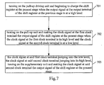
- Embodiments of the present disclosure also provide a gate driving method implemented by taking advantage of the aforesaid gate driving circuit, and the implementation flow of said method can refer to Figure 7 , comprising:
- the high level of the clock signal at said second clock terminal is lower than the high level of the clock signal at said first clock terminal.
- the difference between the high level of the clock signal at said second clock terminal and that of the clock signal at said first clock terminal is determined according to the specific situation of the actual application.
Landscapes
- Engineering & Computer Science (AREA)
- Chemical & Material Sciences (AREA)
- Crystallography & Structural Chemistry (AREA)
- Physics & Mathematics (AREA)
- Computer Hardware Design (AREA)
- General Physics & Mathematics (AREA)
- Theoretical Computer Science (AREA)
- Control Of Indicators Other Than Cathode Ray Tubes (AREA)
- Liquid Crystal Display Device Control (AREA)
- Shift Register Type Memory (AREA)
- Liquid Crystal (AREA)
Claims (10)
- Gate-Ansteuerschaltung mit Schieberegistern an einer Vielzahl von Stufen, wobei die Schieberegister an jeder Stufe eine Pull-Up-Ansteuereinheit, eine Pull-Up-Einheit, eine Reset-Einheit und eine Pull-Down-Einheit, wobei das Schieberegister weiter aufweist: eine Zusatzeinheit aufweisen; wobei
die Pull-Up-Einheit (M3, C1) konfiguriert ist zum Bilden eines Taktsignals an einem ersten Taktanschluss (CLK1) als ein Ausgabesignal des Schieberegisters an der vorliegenden Stufe, wenn es während einer Phase eingeschaltet wird, in der ein Eingangsknoten (PU) der Pull-Up-Einheit sich auf einem H-Pegel befindet, das Taktsignal an dem ersten Taktanschluss (CLK1) sich an seinem H-Pegel befindet und ein Taktsignal an einem zweiten Taktanschluss (CLK2) sich an einem L-Pegel befindet; gekennzeichnet dadurch, dass
die Zusatzeinheit (32), welche mit der Pull-Up-Einheit verbunden ist, konfiguriert ist zum Bilden des Taktsignals an dem zweiten Taktanschluss (CLK2) als das Ausgangssignal des Schieberegisters an der vorliegenden Stufe, wenn es während einer anderen Phase eingeschaltet wird, unmittelbar nach der Phase, in der der Eingangsknoten (PU) der Pull-Up-Einheit auf dem H-Pegel verbleibt, das Taktsignal an dem ersten Taktanschluss (CLK1) auf einen L-Pegel springt und das Taktsignal an dem zweiten Taktanschluss (CLK2) auf seinen H-Pegel springt, wobei der H-Pegel des Taktsignals an dem zweiten Taktanschluss niedriger als der H-Pegel des Taktsignals an dem ersten Taktanschluss ist. - Gate-Ansteuerschaltung gemäß Anspruch 1, wobei die Pull-Up-Ansteuereinheit, die mit dem Eingangsknoten (PU) der Pull-Up-Einheit verbunden ist, zum Steuern des EIN und AUS der Pull-Up-Einheit konfiguriert ist.
- Gate-Ansteuerschaltung gemäß Anspruch 2, wobei die Pull-Up-Ansteuereinheit eine erste TFT-Schaltvorrichtung (M1) und eine zweite TFT-Schaltvorrichtung (M2) aufweist; wobei,
ein Drain und ein Gate der ersten TFT-Schaltvorrichtung (M1) verbunden sind mit einem Ausgangsanschluss (INPUT) des Schieberegisters an einer vorhergehenden Stufe;
ein Drain der zweiten TFT-Schaltvorrichtung (M2) mit der Source der ersten TFT-Schaltvorrichtung (M1) verbunden ist, ein Gate der zweiten TFT-Schaltvorrichtung (M2) mit einem Ausgangsanschluss (RESET) des Schieberegisters an einer nächsten Stufe verbunden ist, und eine Source der zweiten TFT-Schaltvorrichtung mit einem L-Pegel verbunden ist. - Gate-Ansteuerschaltung gemäß Anspruch 3, wobei die Pull-Up-Einheit eine dritte TFT-Schaltvorrichtung (M3) und eine Verstärkervorrichtung (C1) aufweist; wobei
ein Drain der dritten TFT-Schaltvorrichtung (M3) mit dem ersten Taktanschluss (CLK1) verbunden ist, ein Gate der dritten TFT-Schaltvorrichtung (M3) mit der Source der ersten TFT-Schaltvorrichtung (M1) verbunden ist, und eine Source der dritten TFT-Schaltvorrichtung (M3) mit einem Ausgangsanschluss (OUTPUT) des Schieberegisters an der vorliegenden Stufe verbunden ist;
die Verstärkervorrichtung (C1) einen ersten Anschluss aufweist, der jeweils mit der Source der ersten TFT-Schaltvorrichtung (M1) und dem Gate der dritten TFT-Schaltvorrichtung (M3) verbunden ist und ein zweiter Anschluss mit der Source der dritten TFT-Schaltvorrichtung (M3) verbunden ist. - Gate-Ansteuerschaltung gemäß Anspruch 4, wobei die Reset-Einheit eine vierte TFT-Schaltvorrichtung (M4) aufweist; wobei ein Drain der vierten TFT-Schaltvorrichtung (M4) mit der Source der dritten TFT-Schaltvorrichtung (M3) verbunden ist, ein Gate der vierten TFT-Schaltvorrichtung (M4) mit dem Ausgangsanschluss (RESET) des Schieberegisters an der nächsten Stufe verbunden ist, und eine Source der vierten TFT-Schaltvorrichtung (M4) mit einem L-Pegel verbunden ist.
- Gate-Ansteuerschaltung gemäß Anspruch 5, wobei die Zusatzeinheit eine fünfte TFT-Schaltvorrichtung (M5) und eine sechste TFT-Schaltvorrichtung (M6) aufweist; wobei
ein Drain und ein Gate der fünften TFT-Schaltvorrichtung (M5) verbunden sind mit dem zweiten Taktanschluss (CLK2), ein Drain der sechsten TFT-Schaltvorrichtung (M6) verbunden ist mit einer Source der fünften TFT-Schaltvorrichtung (M5), ein Gate der sechsten TFT-Schaltvorrichtung (M6) verbunden ist mit der Source der ersten TFT-Schaltvorrichtung (M1) der Pull-Up-Ansteuereinheit, und eine Source der sechsten TFT-Schaltvorrichtung (M6) verbunden ist mit dem Ausgangsanschluss der Pull-Up-Einheit und auch als der Ausgangsanschluss (OUTPUT) des Schieberegisters an der vorliegenden Stufe dient. - Gate-Ansteuerschaltung gemäß Anspruch 6, wobei die fünfte Schaltvorrichtung (M5) und die sechste TFT-Schaltvorrichtung (M6) Metalloxyd-Halbleiter-Feldeffekttransistoren sind.
- Gate-Ansteuerschaltung gemäß Anspruch 6, wobei das Taktsignal an dem zweiten Taktanschluss (CLK2) in dem Augenblick auf seinen H-Pegel springt, in dem das Taktsignal an dem ersten Taktanschluss (CLK1) den L-Pegel einnimmt.
- Flüssigkristallanzeige mit der Gate-Ansteuerschaltung gemäß einem der Ansprüche 1 bis 8.
- Gate-Ansteuerverfahren für die Gate-Ansteuerschaltung gemäß einem der Ansprüche 1 bis 8, aufweisend:während einer ersten Phase, Einschalten der Pull-Up-Ansteuereinheit und Beginnen das Schieberegister an der vorliegenden Stufe derart zu laden, dass ein Eingangsknoten (PU) der Pull-Up-Einheit sich an einem H-Pegel befindet, wenn das Ausgangssignal an dem Ausgangsanschluss (INPUT) des Schieberegisters an einer vorhergehenden Stufe sich auf einem H-Pegel befindet und sowohl das Taktsignal an dem ersten Taktanschluss (CLK1) als auch das Taktsignal an dem zweiten Taktanschluss (CLK2) sich auf einem L-Pegel befinden;während einer zweiten Phase unmittelbar nach der ersten Phase, das Ausgangssignal an dem Ausgangsanschluss (INPUT) des Schieberegisters an der vorhergehenden Stufe auf den L-Pegel springt, das Taktsignal an dem ersten Taktanschluss (CLK1) auf seinen H-Pegel springt, und das Taktsignal an dem zweiten Taktanschluss (CLK2) auf seinem L-Pegel verbleibt, Einschalten der Pull-Up-Einheit durch den H-Pegel an dem Eingangsknoten (PU) der Pull-Up-Einheit und Bilden des Taktsignals an dem ersten Taktanschluss (CLK1) als das Ausgangssignal des Schieberegisters an der vorliegenden Stufe;während einer dritten Phase, unmittelbar nach der zweiten Phase, Springen des Taktsignals an dem ersten Taktanschluss (CLK1) auf den L-Pegel, Springen des Taktsignals an dem zweiten Taktanschluss (CLK2) auf seinen H-Pegel, Einschalten der Zusatzeinheit durch das Taktsignal an dem zweiten Taktanschluss (CLK2) und des H-Pegels an dem Eingangsknoten (PU) der Pull-Up-Einheit, und Bilden des Taktsignals an dem zweiten Taktanschluss als das Ausgangssignal des Schieberegisters an der vorliegenden Stufe, wobei H-Pegel des Taktsignals an dem zweiten Taktanschluss niedriger als der H-Pegel des Taktsignals an dem ersten Taktanschluss ist.
Applications Claiming Priority (2)
| Application Number | Priority Date | Filing Date | Title |
|---|---|---|---|
| CN201210089393.9A CN102779494B (zh) | 2012-03-29 | 2012-03-29 | 一种栅极驱动电路、方法及液晶显示器 |
| PCT/CN2012/085194 WO2013143307A1 (zh) | 2012-03-29 | 2012-11-23 | 栅极驱动电路、栅极驱动方法及液晶显示器 |
Publications (3)
| Publication Number | Publication Date |
|---|---|
| EP2667376A1 EP2667376A1 (de) | 2013-11-27 |
| EP2667376A4 EP2667376A4 (de) | 2015-06-10 |
| EP2667376B1 true EP2667376B1 (de) | 2017-07-19 |
Family
ID=47124397
Family Applications (1)
| Application Number | Title | Priority Date | Filing Date |
|---|---|---|---|
| EP12842680.6A Active EP2667376B1 (de) | 2012-03-29 | 2012-11-23 | Gate-elektroden-treiberschaltung, gate-elektroden-ansteuerverfahren und flüssigkristallanzeigevorrichtung |
Country Status (6)
| Country | Link |
|---|---|
| US (1) | US9378692B2 (de) |
| EP (1) | EP2667376B1 (de) |
| JP (1) | JP6193969B2 (de) |
| KR (1) | KR101521732B1 (de) |
| CN (1) | CN102779494B (de) |
| WO (1) | WO2013143307A1 (de) |
Families Citing this family (37)
| Publication number | Priority date | Publication date | Assignee | Title |
|---|---|---|---|---|
| CN102779494B (zh) * | 2012-03-29 | 2015-08-05 | 北京京东方光电科技有限公司 | 一种栅极驱动电路、方法及液晶显示器 |
| CN102915714B (zh) * | 2012-10-11 | 2015-05-27 | 京东方科技集团股份有限公司 | 一种移位寄存器、液晶显示栅极驱动装置和液晶显示装置 |
| KR102015396B1 (ko) * | 2012-11-27 | 2019-08-28 | 엘지디스플레이 주식회사 | 쉬프트 레지스터와 이의 구동방법 |
| CN103198783B (zh) * | 2013-04-01 | 2015-04-29 | 京东方科技集团股份有限公司 | 移位寄存器单元、移位寄存器和显示装置 |
| JP6139777B2 (ja) * | 2013-04-02 | 2017-05-31 | ビーオーイー・テクノロジー・グループ・カンパニー・リミテッド | 残像除去装置、ディスプレイ及び残像除去方法 |
| CN103247275B (zh) * | 2013-04-22 | 2015-03-11 | 合肥京东方光电科技有限公司 | 一种移位寄存器单元、栅极驱动电路及阵列基板 |
| CN103258514B (zh) * | 2013-05-06 | 2015-05-20 | 深圳市华星光电技术有限公司 | Goa驱动电路及驱动方法 |
| CN103680388B (zh) * | 2013-12-26 | 2015-11-11 | 深圳市华星光电技术有限公司 | 用于平板显示的可修复的goa电路及显示装置 |
| TWI539435B (zh) | 2014-08-29 | 2016-06-21 | 友達光電股份有限公司 | 驅動電路 |
| CN104240766A (zh) * | 2014-09-26 | 2014-12-24 | 合肥京东方光电科技有限公司 | 移位寄存器单元及栅极驱动装置 |
| CN104575435B (zh) * | 2015-02-05 | 2017-12-15 | 京东方科技集团股份有限公司 | 显示基板栅极线驱动方法及驱动单元、显示装置 |
| KR20160137866A (ko) | 2015-05-22 | 2016-12-01 | 삼성디스플레이 주식회사 | 게이트 구동 장치, 그것을 포함하는 표시 장치 및 그 구동 방법 |
| KR102339648B1 (ko) * | 2015-06-24 | 2021-12-16 | 엘지디스플레이 주식회사 | 게이트 구동회로와 이를 이용한 표시장치 |
| CN204946515U (zh) * | 2015-09-08 | 2016-01-06 | 京东方科技集团股份有限公司 | 阵列基板行驱动goa单元的保护电路和阵列基板 |
| CN105609137B (zh) * | 2016-01-05 | 2019-06-07 | 京东方科技集团股份有限公司 | 移位寄存器、栅线集成驱动电路、阵列基板及显示装置 |
| CN105549289B (zh) * | 2016-03-09 | 2018-12-21 | 武汉华星光电技术有限公司 | 一种阵列基板、显示器和测试系统 |
| US20180161866A1 (en) | 2016-12-13 | 2018-06-14 | General Electric Company | Multi-piece integrated core-shell structure for making cast component |
| US11813669B2 (en) | 2016-12-13 | 2023-11-14 | General Electric Company | Method for making an integrated core-shell structure |
| KR102643465B1 (ko) | 2017-01-17 | 2024-03-05 | 삼성디스플레이 주식회사 | 표시 장치 및 그 구동 방법 |
| CN106782336B (zh) * | 2017-02-07 | 2019-01-22 | 京东方科技集团股份有限公司 | 栅极驱动单元及其驱动方法、栅极驱动电路和显示装置 |
| CN106991984B (zh) * | 2017-05-12 | 2018-05-18 | 惠科股份有限公司 | 移位元暂存电路及其应用的显示面板 |
| CN109389926B (zh) * | 2017-08-11 | 2022-02-25 | 京东方科技集团股份有限公司 | 移位寄存器、栅极驱动电路、阵列基板 |
| KR102508522B1 (ko) | 2017-11-09 | 2023-03-10 | 삼성전자주식회사 | 3차원 반도체 메모리 소자 및 이의 전기적 불량 판별 방법 |
| CN108364622B (zh) * | 2018-04-24 | 2020-11-06 | 京东方科技集团股份有限公司 | 移位寄存器单元及其驱动方法、驱动装置和显示装置 |
| US11205382B2 (en) * | 2018-11-22 | 2021-12-21 | Novatek Microelectronics Corp. | Sensing circuit for OLED driver and OLED driver using the same |
| CN109935188B (zh) * | 2019-03-08 | 2020-11-24 | 合肥京东方卓印科技有限公司 | 栅极驱动单元、方法、栅极驱动模组、电路及显示装置 |
| CN110223655A (zh) * | 2019-06-28 | 2019-09-10 | 昆山龙腾光电有限公司 | 栅极驱动电路及显示装置 |
| CN113450732B (zh) * | 2020-03-25 | 2023-06-02 | Oppo广东移动通信有限公司 | 像素电路及其驱动方法、显示装置、电子设备 |
| US11315473B2 (en) * | 2020-06-16 | 2022-04-26 | Tcl China Star Optoelectronics Technology Co., Ltd. | Gate-on-array driving circuit |
| CN114974163B (zh) * | 2022-06-28 | 2023-05-26 | 惠科股份有限公司 | 扫描驱动电路、阵列基板和显示面板 |
| US12618332B2 (en) | 2022-11-01 | 2026-05-05 | General Electric Company | Gas turbine engine |
| US12196131B2 (en) | 2022-11-01 | 2025-01-14 | General Electric Company | Gas turbine engine |
| US12618378B2 (en) | 2022-11-01 | 2026-05-05 | General Electric Company | Gas turbine engine |
| US12410753B2 (en) | 2022-11-01 | 2025-09-09 | General Electric Company | Gas turbine engine |
| US12503980B2 (en) | 2022-11-01 | 2025-12-23 | General Electric Company | Gas turbine engine |
| US12428992B2 (en) | 2022-11-01 | 2025-09-30 | General Electric Company | Gas turbine engine |
| CN120089107A (zh) * | 2025-04-21 | 2025-06-03 | 昆山龙腾光电股份有限公司 | 栅极驱动电路及显示装置 |
Family Cites Families (22)
| Publication number | Priority date | Publication date | Assignee | Title |
|---|---|---|---|---|
| JP3292520B2 (ja) * | 1991-10-11 | 2002-06-17 | 株式会社東芝 | 液晶表示装置 |
| KR100495798B1 (ko) * | 1997-09-09 | 2005-09-20 | 삼성전자주식회사 | 액정표시장치및킥백전압보상회로 |
| KR100617611B1 (ko) * | 1999-12-30 | 2006-09-01 | 비오이 하이디스 테크놀로지 주식회사 | 다중 레벨을 갖는 게이트 구동 신호 발생 회로 |
| KR100619162B1 (ko) * | 2000-12-30 | 2006-09-05 | 비오이 하이디스 테크놀로지 주식회사 | 액정표시모듈의 저소비전력 구동장치 |
| KR20020091451A (ko) | 2001-05-30 | 2002-12-06 | 주식회사 현대 디스플레이 테크놀로지 | 박막트랜지스터 액정표시장치의 멀티 레벨 게이트구동전압발생회로 |
| GB2397710A (en) * | 2003-01-25 | 2004-07-28 | Sharp Kk | A shift register for an LCD driver, comprising reset-dominant RS flip-flops |
| KR100551729B1 (ko) * | 2003-03-19 | 2006-02-13 | 비오이 하이디스 테크놀로지 주식회사 | 액정표시장치의 게이트 라인 구동방법 및 그 구동회로 |
| US7319452B2 (en) | 2003-03-25 | 2008-01-15 | Samsung Electronics Co., Ltd. | Shift register and display device having the same |
| KR100697387B1 (ko) * | 2004-09-03 | 2007-03-20 | 비오이 하이디스 테크놀로지 주식회사 | 액정표시장치용 쉬프트 레지스터 |
| KR101300038B1 (ko) * | 2006-08-08 | 2013-08-29 | 삼성디스플레이 주식회사 | 게이트 구동회로 및 이를 포함하는 표시 장치 |
| JP4990034B2 (ja) * | 2006-10-03 | 2012-08-01 | 三菱電機株式会社 | シフトレジスタ回路およびそれを備える画像表示装置 |
| KR101281498B1 (ko) | 2006-10-31 | 2013-07-02 | 삼성디스플레이 주식회사 | 게이트 구동회로 및 이를 갖는 표시장치 |
| CN101779227B (zh) * | 2007-10-24 | 2012-03-28 | 夏普株式会社 | 显示面板和显示装置 |
| WO2010067643A1 (ja) * | 2008-12-12 | 2010-06-17 | シャープ株式会社 | シフトレジスタ回路および表示装置ならびにシフトレジスタ回路の駆動方法 |
| KR101579082B1 (ko) * | 2008-12-23 | 2015-12-22 | 삼성디스플레이 주식회사 | 게이트 구동회로 및 이의 구동 방법 |
| TWI406218B (zh) * | 2009-01-09 | 2013-08-21 | Chunghwa Picture Tubes Ltd | 高可靠度閘極驅動電路 |
| CN102012591B (zh) * | 2009-09-04 | 2012-05-30 | 北京京东方光电科技有限公司 | 移位寄存器单元及液晶显示器栅极驱动装置 |
| CN101763900A (zh) * | 2010-01-18 | 2010-06-30 | 友达光电股份有限公司 | 移位寄存器电路 |
| JP5435481B2 (ja) * | 2010-02-26 | 2014-03-05 | 株式会社ジャパンディスプレイ | シフトレジスタ、走査線駆動回路、電気光学装置および電子機器 |
| TWI415099B (zh) * | 2010-11-10 | 2013-11-11 | Au Optronics Corp | 液晶顯示器驅動電路及相關驅動方法 |
| CN202102694U (zh) * | 2011-05-25 | 2012-01-04 | 京东方科技集团股份有限公司 | 一种薄膜晶体管移位寄存器、液晶面板及显示设备 |
| CN102779494B (zh) * | 2012-03-29 | 2015-08-05 | 北京京东方光电科技有限公司 | 一种栅极驱动电路、方法及液晶显示器 |
-
2012
- 2012-03-29 CN CN201210089393.9A patent/CN102779494B/zh active Active
- 2012-11-23 WO PCT/CN2012/085194 patent/WO2013143307A1/zh not_active Ceased
- 2012-11-23 JP JP2015502060A patent/JP6193969B2/ja active Active
- 2012-11-23 US US13/884,713 patent/US9378692B2/en active Active
- 2012-11-23 EP EP12842680.6A patent/EP2667376B1/de active Active
- 2012-11-23 KR KR1020137012244A patent/KR101521732B1/ko active Active
Also Published As
| Publication number | Publication date |
|---|---|
| CN102779494B (zh) | 2015-08-05 |
| JP2015516591A (ja) | 2015-06-11 |
| KR101521732B1 (ko) | 2015-05-28 |
| US9378692B2 (en) | 2016-06-28 |
| WO2013143307A1 (zh) | 2013-10-03 |
| KR20130131332A (ko) | 2013-12-03 |
| US20140111413A1 (en) | 2014-04-24 |
| JP6193969B2 (ja) | 2017-09-06 |
| CN102779494A (zh) | 2012-11-14 |
| EP2667376A1 (de) | 2013-11-27 |
| EP2667376A4 (de) | 2015-06-10 |
Similar Documents
| Publication | Publication Date | Title |
|---|---|---|
| US9378692B2 (en) | Gate driving circuit and method, and liquid crystal display | |
| US9368230B2 (en) | Shift register unit, gate driving circuit, driving method and display apparatus | |
| US9466254B2 (en) | Shift register unit, gate driving circuit and display apparatus | |
| EP2743929B1 (de) | Schieberegistereinheit, Gate-Treiber und Anzeigevorrichtung | |
| KR101443126B1 (ko) | 게이트 드라이버 온 어레이, 시프팅 레지스터 및 디스플레이 스크린 | |
| US8049706B2 (en) | Gate driving circuit capable of suppressing threshold voltage drift | |
| US9530370B2 (en) | Shift register unit and driving method thereof, gate driving circuit and display device | |
| EP2879126B1 (de) | Gate-treiberschaltung, verfahren und flüssigkristallanzeige | |
| US9659540B1 (en) | GOA circuit of reducing power consumption | |
| CN108932933B (zh) | 移位寄存器、栅极驱动电路、显示装置 | |
| US9666152B2 (en) | Shift register unit, gate driving circuit and display device | |
| KR102156769B1 (ko) | 표시장치와 그의 게이트 쉬프트 레지스터 초기화방법 | |
| US10650904B2 (en) | Shift register unit and driving method thereof, gate driving apparatus and display apparatus | |
| CN102682699B (zh) | 栅极驱动电路及显示器 | |
| TWI540554B (zh) | Liquid crystal display device and driving method thereof | |
| US9928797B2 (en) | Shift register unit and driving method thereof, gate driving apparatus and display apparatus | |
| US10096373B2 (en) | Shift register and driving method therefor, gate driver on array circuit and display device | |
| US20180040382A1 (en) | Shift registers and driving methods thereof, gate driving apparatus and display apparatuses | |
| TW200405235A (en) | Shift register and liquid crystal display having the same | |
| US9030397B2 (en) | Gate driver, driving circuit, and LCD | |
| US10685615B2 (en) | Shift register and driving method thereof, gate driving circuit, and display device | |
| JP6555842B2 (ja) | Goa回路及びその駆動方法、液晶ディスプレイ | |
| US20160284309A1 (en) | Semiconductor device and electronic apparatus | |
| KR20180062185A (ko) | 시프트 레지스터 및 이를 이용한 표시장치 | |
| KR102031365B1 (ko) | 스캔 구동부 및 이를 이용한 표시장치 |
Legal Events
| Date | Code | Title | Description |
|---|---|---|---|
| PUAI | Public reference made under article 153(3) epc to a published international application that has entered the european phase |
Free format text: ORIGINAL CODE: 0009012 |
|
| 17P | Request for examination filed |
Effective date: 20130426 |
|
| AK | Designated contracting states |
Kind code of ref document: A1 Designated state(s): AL AT BE BG CH CY CZ DE DK EE ES FI FR GB GR HR HU IE IS IT LI LT LU LV MC MK MT NL NO PL PT RO RS SE SI SK SM TR |
|
| RA4 | Supplementary search report drawn up and despatched (corrected) |
Effective date: 20150512 |
|
| RIC1 | Information provided on ipc code assigned before grant |
Ipc: G02F 1/1368 20060101ALI20150506BHEP Ipc: G11C 19/28 20060101ALI20150506BHEP Ipc: G02F 1/133 20060101ALI20150506BHEP Ipc: G02F 1/1362 20060101ALI20150506BHEP Ipc: G09G 3/36 20060101AFI20150506BHEP |
|
| DAX | Request for extension of the european patent (deleted) | ||
| GRAP | Despatch of communication of intention to grant a patent |
Free format text: ORIGINAL CODE: EPIDOSNIGR1 |
|
| STAA | Information on the status of an ep patent application or granted ep patent |
Free format text: STATUS: GRANT OF PATENT IS INTENDED |
|
| INTG | Intention to grant announced |
Effective date: 20170203 |
|
| GRAS | Grant fee paid |
Free format text: ORIGINAL CODE: EPIDOSNIGR3 |
|
| GRAA | (expected) grant |
Free format text: ORIGINAL CODE: 0009210 |
|
| STAA | Information on the status of an ep patent application or granted ep patent |
Free format text: STATUS: THE PATENT HAS BEEN GRANTED |
|
| AK | Designated contracting states |
Kind code of ref document: B1 Designated state(s): AL AT BE BG CH CY CZ DE DK EE ES FI FR GB GR HR HU IE IS IT LI LT LU LV MC MK MT NL NO PL PT RO RS SE SI SK SM TR |
|
| REG | Reference to a national code |
Ref country code: GB Ref legal event code: FG4D |
|
| REG | Reference to a national code |
Ref country code: CH Ref legal event code: EP |
|
| REG | Reference to a national code |
Ref country code: IE Ref legal event code: FG4D |
|
| REG | Reference to a national code |
Ref country code: AT Ref legal event code: REF Ref document number: 911081 Country of ref document: AT Kind code of ref document: T Effective date: 20170815 |
|
| REG | Reference to a national code |
Ref country code: NL Ref legal event code: FP |
|
| REG | Reference to a national code |
Ref country code: DE Ref legal event code: R096 Ref document number: 602012034856 Country of ref document: DE |
|
| REG | Reference to a national code |
Ref country code: FR Ref legal event code: PLFP Year of fee payment: 6 |
|
| REG | Reference to a national code |
Ref country code: LT Ref legal event code: MG4D |
|
| REG | Reference to a national code |
Ref country code: AT Ref legal event code: MK05 Ref document number: 911081 Country of ref document: AT Kind code of ref document: T Effective date: 20170719 |
|
| PG25 | Lapsed in a contracting state [announced via postgrant information from national office to epo] |
Ref country code: FI Free format text: LAPSE BECAUSE OF FAILURE TO SUBMIT A TRANSLATION OF THE DESCRIPTION OR TO PAY THE FEE WITHIN THE PRESCRIBED TIME-LIMIT Effective date: 20170719 Ref country code: SE Free format text: LAPSE BECAUSE OF FAILURE TO SUBMIT A TRANSLATION OF THE DESCRIPTION OR TO PAY THE FEE WITHIN THE PRESCRIBED TIME-LIMIT Effective date: 20170719 Ref country code: HR Free format text: LAPSE BECAUSE OF FAILURE TO SUBMIT A TRANSLATION OF THE DESCRIPTION OR TO PAY THE FEE WITHIN THE PRESCRIBED TIME-LIMIT Effective date: 20170719 Ref country code: NO Free format text: LAPSE BECAUSE OF FAILURE TO SUBMIT A TRANSLATION OF THE DESCRIPTION OR TO PAY THE FEE WITHIN THE PRESCRIBED TIME-LIMIT Effective date: 20171019 Ref country code: LT Free format text: LAPSE BECAUSE OF FAILURE TO SUBMIT A TRANSLATION OF THE DESCRIPTION OR TO PAY THE FEE WITHIN THE PRESCRIBED TIME-LIMIT Effective date: 20170719 Ref country code: AT Free format text: LAPSE BECAUSE OF FAILURE TO SUBMIT A TRANSLATION OF THE DESCRIPTION OR TO PAY THE FEE WITHIN THE PRESCRIBED TIME-LIMIT Effective date: 20170719 |
|
| PG25 | Lapsed in a contracting state [announced via postgrant information from national office to epo] |
Ref country code: LV Free format text: LAPSE BECAUSE OF FAILURE TO SUBMIT A TRANSLATION OF THE DESCRIPTION OR TO PAY THE FEE WITHIN THE PRESCRIBED TIME-LIMIT Effective date: 20170719 Ref country code: BG Free format text: LAPSE BECAUSE OF FAILURE TO SUBMIT A TRANSLATION OF THE DESCRIPTION OR TO PAY THE FEE WITHIN THE PRESCRIBED TIME-LIMIT Effective date: 20171019 Ref country code: RS Free format text: LAPSE BECAUSE OF FAILURE TO SUBMIT A TRANSLATION OF THE DESCRIPTION OR TO PAY THE FEE WITHIN THE PRESCRIBED TIME-LIMIT Effective date: 20170719 Ref country code: ES Free format text: LAPSE BECAUSE OF FAILURE TO SUBMIT A TRANSLATION OF THE DESCRIPTION OR TO PAY THE FEE WITHIN THE PRESCRIBED TIME-LIMIT Effective date: 20170719 Ref country code: GR Free format text: LAPSE BECAUSE OF FAILURE TO SUBMIT A TRANSLATION OF THE DESCRIPTION OR TO PAY THE FEE WITHIN THE PRESCRIBED TIME-LIMIT Effective date: 20171020 Ref country code: IS Free format text: LAPSE BECAUSE OF FAILURE TO SUBMIT A TRANSLATION OF THE DESCRIPTION OR TO PAY THE FEE WITHIN THE PRESCRIBED TIME-LIMIT Effective date: 20171119 Ref country code: PL Free format text: LAPSE BECAUSE OF FAILURE TO SUBMIT A TRANSLATION OF THE DESCRIPTION OR TO PAY THE FEE WITHIN THE PRESCRIBED TIME-LIMIT Effective date: 20170719 |
|
| REG | Reference to a national code |
Ref country code: DE Ref legal event code: R097 Ref document number: 602012034856 Country of ref document: DE |
|
| PG25 | Lapsed in a contracting state [announced via postgrant information from national office to epo] |
Ref country code: RO Free format text: LAPSE BECAUSE OF FAILURE TO SUBMIT A TRANSLATION OF THE DESCRIPTION OR TO PAY THE FEE WITHIN THE PRESCRIBED TIME-LIMIT Effective date: 20170719 Ref country code: DK Free format text: LAPSE BECAUSE OF FAILURE TO SUBMIT A TRANSLATION OF THE DESCRIPTION OR TO PAY THE FEE WITHIN THE PRESCRIBED TIME-LIMIT Effective date: 20170719 Ref country code: CZ Free format text: LAPSE BECAUSE OF FAILURE TO SUBMIT A TRANSLATION OF THE DESCRIPTION OR TO PAY THE FEE WITHIN THE PRESCRIBED TIME-LIMIT Effective date: 20170719 |
|
| PLBE | No opposition filed within time limit |
Free format text: ORIGINAL CODE: 0009261 |
|
| STAA | Information on the status of an ep patent application or granted ep patent |
Free format text: STATUS: NO OPPOSITION FILED WITHIN TIME LIMIT |
|
| PG25 | Lapsed in a contracting state [announced via postgrant information from national office to epo] |
Ref country code: EE Free format text: LAPSE BECAUSE OF FAILURE TO SUBMIT A TRANSLATION OF THE DESCRIPTION OR TO PAY THE FEE WITHIN THE PRESCRIBED TIME-LIMIT Effective date: 20170719 Ref country code: SM Free format text: LAPSE BECAUSE OF FAILURE TO SUBMIT A TRANSLATION OF THE DESCRIPTION OR TO PAY THE FEE WITHIN THE PRESCRIBED TIME-LIMIT Effective date: 20170719 Ref country code: IT Free format text: LAPSE BECAUSE OF FAILURE TO SUBMIT A TRANSLATION OF THE DESCRIPTION OR TO PAY THE FEE WITHIN THE PRESCRIBED TIME-LIMIT Effective date: 20170719 Ref country code: SK Free format text: LAPSE BECAUSE OF FAILURE TO SUBMIT A TRANSLATION OF THE DESCRIPTION OR TO PAY THE FEE WITHIN THE PRESCRIBED TIME-LIMIT Effective date: 20170719 |
|
| 26N | No opposition filed |
Effective date: 20180420 |
|
| PG25 | Lapsed in a contracting state [announced via postgrant information from national office to epo] |
Ref country code: MC Free format text: LAPSE BECAUSE OF FAILURE TO SUBMIT A TRANSLATION OF THE DESCRIPTION OR TO PAY THE FEE WITHIN THE PRESCRIBED TIME-LIMIT Effective date: 20170719 |
|
| PG25 | Lapsed in a contracting state [announced via postgrant information from national office to epo] |
Ref country code: CH Free format text: LAPSE BECAUSE OF NON-PAYMENT OF DUE FEES Effective date: 20171130 Ref country code: LI Free format text: LAPSE BECAUSE OF NON-PAYMENT OF DUE FEES Effective date: 20171130 |
|
| PG25 | Lapsed in a contracting state [announced via postgrant information from national office to epo] |
Ref country code: SI Free format text: LAPSE BECAUSE OF FAILURE TO SUBMIT A TRANSLATION OF THE DESCRIPTION OR TO PAY THE FEE WITHIN THE PRESCRIBED TIME-LIMIT Effective date: 20170719 Ref country code: LU Free format text: LAPSE BECAUSE OF NON-PAYMENT OF DUE FEES Effective date: 20171123 |
|
| REG | Reference to a national code |
Ref country code: BE Ref legal event code: MM Effective date: 20171130 |
|
| REG | Reference to a national code |
Ref country code: IE Ref legal event code: MM4A |
|
| PG25 | Lapsed in a contracting state [announced via postgrant information from national office to epo] |
Ref country code: MT Free format text: LAPSE BECAUSE OF NON-PAYMENT OF DUE FEES Effective date: 20171123 |
|
| REG | Reference to a national code |
Ref country code: FR Ref legal event code: PLFP Year of fee payment: 7 |
|
| PG25 | Lapsed in a contracting state [announced via postgrant information from national office to epo] |
Ref country code: IE Free format text: LAPSE BECAUSE OF NON-PAYMENT OF DUE FEES Effective date: 20171123 |
|
| PG25 | Lapsed in a contracting state [announced via postgrant information from national office to epo] |
Ref country code: BE Free format text: LAPSE BECAUSE OF NON-PAYMENT OF DUE FEES Effective date: 20171130 |
|
| PG25 | Lapsed in a contracting state [announced via postgrant information from national office to epo] |
Ref country code: HU Free format text: LAPSE BECAUSE OF FAILURE TO SUBMIT A TRANSLATION OF THE DESCRIPTION OR TO PAY THE FEE WITHIN THE PRESCRIBED TIME-LIMIT; INVALID AB INITIO Effective date: 20121123 |
|
| PG25 | Lapsed in a contracting state [announced via postgrant information from national office to epo] |
Ref country code: CY Free format text: LAPSE BECAUSE OF NON-PAYMENT OF DUE FEES Effective date: 20170719 |
|
| PG25 | Lapsed in a contracting state [announced via postgrant information from national office to epo] |
Ref country code: MK Free format text: LAPSE BECAUSE OF FAILURE TO SUBMIT A TRANSLATION OF THE DESCRIPTION OR TO PAY THE FEE WITHIN THE PRESCRIBED TIME-LIMIT Effective date: 20170719 |
|
| PG25 | Lapsed in a contracting state [announced via postgrant information from national office to epo] |
Ref country code: TR Free format text: LAPSE BECAUSE OF FAILURE TO SUBMIT A TRANSLATION OF THE DESCRIPTION OR TO PAY THE FEE WITHIN THE PRESCRIBED TIME-LIMIT Effective date: 20170719 |
|
| PG25 | Lapsed in a contracting state [announced via postgrant information from national office to epo] |
Ref country code: PT Free format text: LAPSE BECAUSE OF FAILURE TO SUBMIT A TRANSLATION OF THE DESCRIPTION OR TO PAY THE FEE WITHIN THE PRESCRIBED TIME-LIMIT Effective date: 20170719 |
|
| PG25 | Lapsed in a contracting state [announced via postgrant information from national office to epo] |
Ref country code: AL Free format text: LAPSE BECAUSE OF FAILURE TO SUBMIT A TRANSLATION OF THE DESCRIPTION OR TO PAY THE FEE WITHIN THE PRESCRIBED TIME-LIMIT Effective date: 20170719 |
|
| PGFP | Annual fee paid to national office [announced via postgrant information from national office to epo] |
Ref country code: NL Payment date: 20251117 Year of fee payment: 14 |
|
| PGFP | Annual fee paid to national office [announced via postgrant information from national office to epo] |
Ref country code: DE Payment date: 20251121 Year of fee payment: 14 |
|
| PGFP | Annual fee paid to national office [announced via postgrant information from national office to epo] |
Ref country code: GB Payment date: 20251117 Year of fee payment: 14 |
|
| PGFP | Annual fee paid to national office [announced via postgrant information from national office to epo] |
Ref country code: FR Payment date: 20251117 Year of fee payment: 14 |