EP2668723B1 - Frequenzteiler mit synchroner bereichserweiterung über oktavengrenzen - Google Patents
Frequenzteiler mit synchroner bereichserweiterung über oktavengrenzen Download PDFInfo
- Publication number
- EP2668723B1 EP2668723B1 EP12703652.3A EP12703652A EP2668723B1 EP 2668723 B1 EP2668723 B1 EP 2668723B1 EP 12703652 A EP12703652 A EP 12703652A EP 2668723 B1 EP2668723 B1 EP 2668723B1
- Authority
- EP
- European Patent Office
- Prior art keywords
- divide
- input
- frequency divider
- cell
- circuit
- Prior art date
- Legal status (The legal status is an assumption and is not a legal conclusion. Google has not performed a legal analysis and makes no representation as to the accuracy of the status listed.)
- Active
Links
Images








Classifications
-
- H—ELECTRICITY
- H03—ELECTRONIC CIRCUITRY
- H03L—AUTOMATIC CONTROL, STARTING, SYNCHRONISATION OR STABILISATION OF GENERATORS OF ELECTRONIC OSCILLATIONS OR PULSES
- H03L7/00—Automatic control of frequency or phase; Synchronisation
- H03L7/06—Automatic control of frequency or phase; Synchronisation using a reference signal applied to a frequency- or phase-locked loop
- H03L7/16—Indirect frequency synthesis, i.e. generating a desired one of a number of predetermined frequencies using a frequency- or phase-locked loop
- H03L7/18—Indirect frequency synthesis, i.e. generating a desired one of a number of predetermined frequencies using a frequency- or phase-locked loop using a frequency divider or counter in the loop
- H03L7/183—Indirect frequency synthesis, i.e. generating a desired one of a number of predetermined frequencies using a frequency- or phase-locked loop using a frequency divider or counter in the loop a time difference being used for locking the loop, the counter counting between fixed numbers or the frequency divider dividing by a fixed number
- H03L7/193—Indirect frequency synthesis, i.e. generating a desired one of a number of predetermined frequencies using a frequency- or phase-locked loop using a frequency divider or counter in the loop a time difference being used for locking the loop, the counter counting between fixed numbers or the frequency divider dividing by a fixed number the frequency divider/counter comprising a commutable pre-divider, e.g. a two modulus divider
-
- G—PHYSICS
- G06—COMPUTING OR CALCULATING; COUNTING
- G06F—ELECTRIC DIGITAL DATA PROCESSING
- G06F1/00—Details not covered by groups G06F3/00 - G06F13/00 and G06F21/00
- G06F1/04—Generating or distributing clock signals or signals derived directly therefrom
-
- G—PHYSICS
- G06—COMPUTING OR CALCULATING; COUNTING
- G06F—ELECTRIC DIGITAL DATA PROCESSING
- G06F1/00—Details not covered by groups G06F3/00 - G06F13/00 and G06F21/00
- G06F1/04—Generating or distributing clock signals or signals derived directly therefrom
- G06F1/08—Clock generators with changeable or programmable clock frequency
-
- H—ELECTRICITY
- H03—ELECTRONIC CIRCUITRY
- H03K—PULSE TECHNIQUE
- H03K23/00—Pulse counters comprising counting chains; Frequency dividers comprising counting chains
- H03K23/64—Pulse counters comprising counting chains; Frequency dividers comprising counting chains with a base or radix other than a power of two
- H03K23/66—Pulse counters comprising counting chains; Frequency dividers comprising counting chains with a base or radix other than a power of two with a variable counting base, e.g. by presetting or by adding or suppressing pulses
- H03K23/667—Pulse counters comprising counting chains; Frequency dividers comprising counting chains with a base or radix other than a power of two with a variable counting base, e.g. by presetting or by adding or suppressing pulses by switching the base during a counting cycle
Definitions
- the present invention relates generally to frequency dividers, and in particular to a circuit apparatus for dividing an input signal with synchronous range extension across octave boundaries.
- FIG. 1 shows an example MMD application in a phase locked loop (PLL).
- PLL 100 includes voltage controlled oscillator (VCO) 160 and crystal reference oscillator 110.
- VCO 160 is divided in frequency by N (in block 180) and crystal reference oscillator 110 is divided in frequency by R (in block 120).
- Fout and Fref are fixed leading to the divider divisor requirement.
- N varies accordingly.
- operation of a divider over a large range of N is desirable. Due to the non-integer relationship between Fout and Fref, correct divider operation during divider dithering or programming word variation is required. Otherwise incorrect average frequencies and spurs would result. Delta sigma modulation is one possible means of varying the divider values to effectively synthesize a non-integer MMD divisor.
- FIG. 2A A commonly used MMD architecture was first published in " A Family of Low-Power Truly Modular Programmable Dividers in Standard 0.35- um CMOS Technology," by Cicero Vaucher in the IEEE Journal of Solid-State Circuits in July 2000 , and is shown in FIG. 2A .
- the basic architecture consists of a cascade of divide-by-2/3 cells. The overall circuit will divide by values of 2 n to (2 n+1 -1), where n is the number of 2/3 cells. This range is almost one octave.
- 2A divider would be capable of dividing by a range of 16-to-31. If more than an octave range is desired then the circuit of FIG. 2B can be used to add "extended division range".
- the architecture based on the cascade of divide-by-2/3 cells has several advantages. Since the 2/3 cells are not all clocked in parallel or at the same frequency, current can be scaled down in successive stages. The dominant current consumption and the most stringent timing will be restricted to the first stage, similar to a ripple divider. But unlike a ripple divider, there is an output near the first stage which is clocked at high frequency. This has phase noise advantages as opposed to using an output at the back end of the cascade where slew rates are lower and jitter can be accumulated. In general the output of Figure 2A could be taken at any of the modout signals or Fo n . They all have frequency equal to Fin/N, where N is the divider programmed word.
- FIG. 3A shows a circuit diagram of D flip-flop 310 used to create a divide-by-2 circuit.
- FIG. 3B shows a circuit diagram of a different implementation used to create a divide-by-2 circuit.
- Master latch (320) and slave latch (330) are used to create a divide-by-2 circuit that is positive-edge triggered.
- FIG. 3C shows a circuit diagram of a third implementation used to create a divide-by-2 circuit.
- Master latch (340) and slave latch (350) are used to create a divide-by-2 circuit that is negative-edge triggered.
- Figures 3A-C may be referred to as "Johnson counters" since the output of the last latch is inverted and fed back as an input to the first latch.
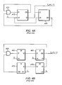
- FIG. 4A shows a circuit diagram of a divide-by-3 circuit implemented with two D flip-flops (415 and 420) and a two-input AND gate 410.
- FIG. 4B shows a different implementation of a divide-by-3 circuit, using master latches 460 and 475, slave latches 465 and 470, and two-input AND gate 455.
- FIG. 4B illustrates a negative-edge triggered implementation of a divide-by-3 circuit, such that the output frequency (f out ) will only transition on the negative edges of the input frequency (f in ).
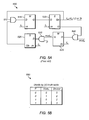
- FIG. 5A illustrates a circuit diagram of a divide-by-2/3 cell used in the architecture described by Vaucher.
- Circuit 500 may divide the input frequency (f in ) by a divisor of either two or three to generate the output frequency (f out ).
- Two control nodes, modulus control input (mode in ) and programming input (P), determine the selection of the divisor for circuit 500.
- Circuit 500 includes two master latches (515 and 535), two slave latches (520 and 525), and three two-input AND gates (510, 530, and 540).
- Master latches 515 and 535 are enabled when the input clock (port label CK) is high (i.e., logic '1', Vcc), and slave latches 520 and 525 are enabled when the input clock is low (i.e., logic '0', ground (GND)).
- FIG. 5B illustrates a truth table for circuit 500 of FIG. 5A .
- the truth table 550 contains columns for control signals P and mod in and for the divisor.
- the divisor represents the value (either 2 or 3) the input frequency of circuit 500 will be divided by to generate the output frequency.
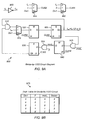
- FIG. 6A illustrates a divide-by-2/3 cell set to divide-by-2 mode.
- divide-by-2 mode either signal mod in or P or both are set to '0', which sets the divisor of circuit 600 as '2'. If control signal mod in is '0', then the signal passing through master latch 635, AND gate 630, and into port D of slave latch 625 will be '0'. If control signal P is '0', then the signal passing through AND gate 630 and into port D of slave latch 625 will be '0'. In either case, the signal output from port Qb of slave latch 625 will be '1'.
- Port Qb of slave latch 625 connects to one of the inputs of AND gate 610, and so if Qb of slave latch 625 is '1', then circuit 600 will function as though latches 625 and 635 were not part of circuit 600, and as if the Qb port of latch 620 were directly connected to the D port of latch 615. In this case, circuit 600 will behave like the functional equivalent of the circuit from FIG. 3C .
- FIG. 6B illustrates a divide-by-2/3 cell set to divide-by-3 mode.
- the signals mod in and P are both set to '1', which sets the divisor of circuit 650 as '3'. Since control signals mod in and P are both '1', circuit, 650 will behave like the functional equivalent of the circuit in FIG. 4B .
- FIG. 7A shows a schematic diagram of a divider with range 4-to-15 as described by Vaucher.
- Divider 700 is a two octave divider utilizing the "extended division range" technique of FIG. 2B .
- Divider 700 includes three stages of division, and each stage includes a divide-by-2/3 cell.
- Each divide-by-2/3 cell has five nodes, which include a first input node (fin), a second input node (mod in ), a third input node (P), a first output node (Fo23), and a second output node (mod out ).
- the fin node of the first divide-by-2/3 cell (710) is coupled to the frequency input to divider 700.
- the Fo23 node of cell 710 is coupled to the fin node of the second divide-by-2/3 cell (715).
- the fin node of each stage is coupled to the Fo23 node of the preceding stage.
- the mod in node of cell 710 is coupled to the mod out node of cell 715.
- the mod out node of cell 725 is coupled to an input to the two-input OR gate 720.
- the other input of OR gate 720 is coupled to inverted control signal P3.
- FIG. 7B illustrates a truth table for divider 700 (of FIG. 7A ) with divisor range 4-to-15.
- Truth table 750 includes columns for the divisor, signals P0-P3, mod2in, and the stage 3 divisor.
- the divisor takes on all integer values from 4 to 15 in truth table 750.
- FIG. 8 shows a schematic diagram of a divider chain with an extended division range.
- the schematic diagram in FIG. 8 is described by Neurauter et al. in U.S. Patent No. 7,109,762 "Frequency-Dividing Circuit Arrangement and Phase Locked Loop Employing such Circuit Arrangement".
- Divider 800 has a divisor range of 4-to-15.
- Divider 800 has four division cells 852, 860, 868, and 876. The first two cells (852 and 860) of the divider chain are divide-by-2/3 cells and the last two cells (868 and 876) are divide-by-1/2/3 cells.
- Divider 800 also includes AND gates 854, 856, 862, 864, 870, 872, 878, and 880 and inverters 858, 866, 874, and 882.
- divider 800 is able to extend the divisor range to greater than an octave.
- the divisor range of a divider described by Neurauter is extended to the range of 2 j to (2 i - 1), where 'j' represents the number of divide-by-2/3 cells and 'i' represents the total number of divide-by-2/3 cells and divide-by-1/2/3 cells. Therefore, for circuit 800 of FIG. 8 , 'j' is two and 'i' is four and the divisor range is 4-to-15.
- a frequency divider comprising a series divide-by-2/3 cells and a divide-by-1/1.5 cell, is disclosed by the publication YANG ET AL: "A Quantization Noise Suppression Technique for Fractional-Frequency Synthesizers", IEEE JOURNAL OF SOLID-STATE CIRCUITS, IEEE SERVICE CENTER, PISCATAWAY, NJ, USA, vol. 41, no. 11, 1 November 2006 (2006-11-01), pages 2500-2511, ISSN: 0018-9200 , DOI: 10.1109/JSSC.2006.883325.
- a frequency divider includes a series of divide-by-2/3 cells and divide-by-1/2/3 cells coupled together.
- the series of divide-by-2/3 cells and divide-by-1/2/3 cells may be cascaded together to create an extended division range for the frequency divider, such that the extended division range spans more than one octave.
- the effective range of possible divisor values N may be determined by the formula 2 j ⁇ N ⁇ (2 (i+1) - 1), wherein j represents the number of divide-by-2/3 cells and wherein i represents the total number of divide-by-2/3 cells and divide-by-1/2/3 cells. Any number of divide-by-2/3 cells and divide-by-1/2/3 cells may be cascaded together to create a frequency divider with a preferred division range.
- the divider circuit including the series of divide-by-2/3 cells and divide-by-1/2/3 cells may be designed such that the circuit does not suffer from any discontinuities while transitioning across a (2 n -1)-to-2 n octave boundary, wherein n is a positive integer.
- the divider circuit may correctly divide by the value specified by a programming word even while the programming word is transitioning across an octave boundary on successive clock cycles.
- the divider circuit may include a corresponding latch, inverter gate, and two-input OR gate.
- a Div1 node of the divide-by-1/2/3 cell may be coupled to a first input node of the two-input OR gate and to a Qb node of the latch.
- a mod out port of each divide-by-1/2/3 cell may be coupled to a second input node of the two-input OR gate and to the input node of the inverter gate.
- the output node of the inverter gate may be coupled to a clock port of the latch.
- the P control signal corresponding to the subsequent divide-by-1/2/3 cell may be coupled to the D node of the latch.
- a mod in port of each divide-by-1/2/3 cell may be coupled to an output node of the two-input OR gate corresponding to a subsequent divide-by-1/2/3 cell.
- the mod in port may be coupled to a high logic level.
- the two highest P control signals corresponding to the two MSB's of the programming divisor word may be coupled to the input nodes of a first two-input OR gate.
- the output of the first two-input OR gate may be coupled to an input node of a second two-input OR gate and to the D node of the latch corresponding to the next to last divide-by-1/2/3 cell in the series of cells.
- the third MSB of the P control signals may be coupled to the other input of the second two-input OR gate.
- the frequency divider described herein may be utilized in a variety of applications, including as a prescaler or multi-modulus divider (MMD).
- MMD multi-modulus divider
- the frequency divider may also be utilized in a frequency synthesizer, phase locked loop (PLL), fractional-N frequency synthesizer, receiver, transmitter, or transceiver.
- PLL phase locked loop
- the frequency divider may also be utilized as part of a radio, including a multi-standard or multi-mode radio, cognitive radio, or software defined radio (SDR).
- SDR software defined radio
- FIG. 9A illustrates one embodiment of a circuit diagram of a divide-by-1/2/3 circuit.
- Divide-by-1/2/3 circuit 900 includes the following elements: three two-to-one multiplexers (915, 955, and 960), three two-input AND gates (910, 935, and 945), one inverter (950), two master latches (920 and 940), and two slave latches (925 and 930).
- the input nodes of circuit 900 include the following: an input frequency (f in ) and three control signals (Div1, mod in , and P).
- the divisor of circuit 900 may be set by the three control signals.
- the output nodes of circuit 900 include the following: f out and mod out .
- the f out node may output a signal with a frequency equal to the input frequency (f in ) divided by one, two, or three.
- the mod out node may be coupled to the mod in node of a preceding cell within a larger divider circuit composed of a series of divide by 2/3 and divide-by-1/2/3 cells.
- the output of two-to-one multiplexer 955 is signal CLKM.
- Signal CLKM connects to node ck of master latches 920 and 940.
- the inputs to multiplexer 955 are the following: f in is coupled to the "0" node, logic '1' is coupled to the "1" node, and Div1 is coupled to the "sel" (select) node.
- the output of two-to-one multiplexer 960 is signal CLKS.
- Signal CLKS is coupled to node ck of slave latches 925 and 930.
- the inputs to multiplexer 960 are the following: f in is coupled to the "0" node, logic '0' is coupled to the "1" node, and Div1 is coupled to the "sel” node.
- Master latches 920 and 940 are active high latches (i.e., the value coupled to input node (D) passes through to the output nodes (Q and Qb) when logic '1' is present at node ck).
- a convention used herein of appending a "b" to the end of a signal name signifies that the signal has been inverted.
- the signal coupled to node Qb is the inverse of the signal coupled to node Q.
- Slave latches 925 and 930 are active low latches (i.e., the value coupled to input node (D) passes through to the outputs nodes (Q and Qb) when logic '0' is present at node ck).
- the Qb node of slave latch 925 is coupled to one of the inputs of two-input AND gate 910, and the Qb node of slave latch 930 is coupled to the other input of AND gate 910.
- the output of AND gate 910 is coupled to the '0' node of multiplexer 915.
- the '1' node of multiplexer 915 is coupled to the output node of inverter 950, which is labeled "f inb " in FIG. 9A .
- the 'sel' node of multiplexer 915 is coupled to input signal "Div1".
- the output node of multiplexer 915 is coupled to the D node of master latch 920.
- circuit elements in circuit 900 may be replaced individually or collectively with other functionally equivalent circuit elements.
- latches 920-940 may be replaced by registers or flip-flops.
- inverter 950 may be replaced by a two-input NAND gate with both inputs tied together.
- Divide-by-1/2/3 circuit 900 may be incorporated into a larger circuit with a series of divide-by-2/3 and divide-by-1/2/3 cells; the larger circuit may be used for dividing a clock frequency by an extended range of divisors.
- truth table 970 includes four columns, with three columns for the following three control signals: Div1, P, and mod in .
- the fourth column of truth table 970 shows the divisor value by which the input frequency to circuit 900 will be divided to generate the output frequency, with the divisor value set by the three control signals.
- Div1 is '0'
- the control signals P and mod in select a divisor value of two or three.
- the divisor has a value of one.
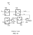
- Circuit 1000 generates an output frequency (fout) at the same frequency as the input frequency (fin).
- Circuit 1000 is an equivalent circuit to circuit 900, and some of the circuit elements (multiplexers, inverter, AND gate) are not shown for the purpose of simplicity.
- the input control signals to circuit 1000 are the following: Div1 is '1', P is '1', and mod in is '1'.
- Div1 is '1'
- P is '1'
- mod in is '1'.
- P and mod in are set to '1' for ease of illustration. However, both signals may also be set to '0' and circuit 1000 will also remain in divide-by-1 mode.
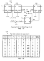
- circuit 1100 may not suffer from a discontinuity (i.e., incorrect value of a divisor) when transitioning across a 2 n -1 to 2 n boundary.
- Circuit 1100 includes divide-by-2/3 cells 1110 and 1115 and divide-by-1/2/3 cell 1125. These three cells are arranged in a series with signals coupled between consecutive elements. Divide-by-2/3 cells 1110 and 1115 may be implemented using circuit 500 of FIG. 5A .
- circuit 500 is only one possible embodiment of a divide-by-2/3 cell which may be used, and other types of divide-by-2/3 cells may also be used with the approaches and mechanisms described herein.
- alternative divide-by-2/3 cells may use flip-flops instead of latches.
- Other types and configurations of divide-by-2/3 cells are also possible.
- Divide-by-1/2/3 cell 1125 may be implemented using circuit 900 of FIG. 9A .
- divide-by-1/2/3 cell 1125 may be implemented using different circuit elements, structures, or configurations than those of circuit 900.
- Circuit 1100 also includes two-input OR gate 1120, latch 1130, and inverter 1135.
- an active low latch may be substituted for latch 1130 and inverter 1135.
- circuit elements 1120, 1130, and 1135 may be replaced individually or collectively with other functionally equivalent circuit elements.
- two-input OR gate 1120 may be replaced by a two-input NAND gate with inverters coupled to each of the two inputs.
- Type latch 1130 may be replaced by one or more latches, registers, and/or flip-flops. Other structures of circuit elements may be arranged that are the functional equivalent of circuit 1100.
- the first circuit element in the cascaded series of dividers of circuit 1100 is divide-by-2/3 cell 1110.
- the frequency input to cell 1110 is the input frequency (f in ) to circuit 1100; f in is the frequency being divided by circuit 1100.
- the frequency output port (Fo23) of cell 1110 is coupled to the frequency input port (fin) of divide-by-2/3 cell 1115.
- the mod in port of cell 1110 is coupled to the mod out port of cell 1115.
- the frequency output port (f out ) of circuit 1100 is tapped off of the mod in port of cell 1110.
- the frequency output port (Fo23) of cell 1115 is coupled to the frequency input port (fin) of divide-by-1/2/3 cell 1125.
- the mod in port of cell 1115 is coupled to the output port of OR gate 1120.
- the mod in port of cell 1115 is also labeled with the signal name "mod2in" in FIG. 11A .
- the frequency output port (Fo123) of cell 1125 and the mod out port of cell 1110 are left unconnected or floating.
- Cell 1110 is the first cell in the series of cells in circuit 1100, and therefore, the mod out port of cell 1110 may be unconnected.
- Cell 1125 is the last cell in the series of cells in circuit 1100, and therefore, the frequency output port (Fo123) of cell 1125 may be unconnected.
- the mod in port of cell 1125 is coupled to logic '1'.
- the DIV1 port of cell 1125 is coupled to the Qb output port of latch 1130.
- the mod out port of cell 1125 (also labeled with the signal name "mod2") is coupled to one of the input ports of OR gate 1120 and to the input port of inverter 1135.
- the output port of inverter 1135 (mod2b) is coupled to the ck port of latch 1130.
- the ck port of latch 1130 may also be referred to as the clock, enable, or clock enable port.
- Latch 1130 includes four ports.
- the Q port is left unconnected or floating.
- the Qb output port is connected to the DIV1 port of cell 1125.
- the Qb output port is also connected to one of the inputs of the two-input OR gate 1120.
- the clock port on latch 1130 is connected to the output of inverter 1135.
- the input to inverter 1135 is connected to the mod out port of the cell 1125.
- the four control signals P0, P1, P2, and P3, are the signals of the programming divisor word that select the value of the divisor.
- the signals P0-P3 may be generated from a control or decoder circuit (not shown).
- the divisor may be any integer value between four and fifteen, and the divisor may change on each f out cycle.
- P0 connects to the P port of cell 1110
- P1 connects to the P port of cell 1115
- P2 connects to the P port of the cell 1125
- P3 connects to the D port of latch 1130.
- Circuit 1100 of FIG. 11a may be expanded to create other clock dividing circuits with different divisor ranges. More 2/3 and 1/2/3 divider cells may be added to the series of cells to create different ranges of possible divisors. Also, a two-input OR gate, latch, and inverter may be added for each 1/2/3 divider cell added to the series.
- the effective range of possible divisor values 'N' may be determined by the formula 2 j ⁇ N ⁇ 2( i+1 ) - 1, where 'j' represents the number of divide-by-2/3 cells and 'i' represents the total number of divide-by-2/3 cells and divide-by-1/2/3 cells. As compared to the prior art of FIG. 8 , circuit 1100 achieves the same range of divisor values (4-to-15) with one less divide-by-1/2/3 cell.
- circuit elements of circuit 1100 may be implemented using any of a variety of types of logic gates, including transistor-transistor logic (TTL), complementary metal-oxide-semiconductor (CMOS), emitter-coupled logic (ECL), positive emitter-coupled logic (PECL), current-mode logic (CML), and others.
- TTL transistor-transistor logic
- CMOS complementary metal-oxide-semiconductor
- ECL emitter-coupled logic
- PECL positive emitter-coupled logic
- CML current-mode logic
- the signals passing between circuit elements may be implemented as single-ended signals or differential signals.
- Circuit 1100 may be utilized as a prescaler or as a multi-modulus divider (MMD). Circuit 1100 may also be utilized in a frequency synthesizer, fractional-N frequency synthesizer, phase locked loop (PLL), receiver, transmitter, or transceiver. In addition, circuit 1100 may also be utilized as part of a radio (e.g., multi-standard radio, multi-mode radio, cognitive radio, software defined radio (SDR)). Other utilizations of circuit 1100 are possible and are contemplated.
- a radio e.g., multi-standard radio, multi-mode radio, cognitive radio, software defined radio (SDR)
- Circuit 1100 may be implemented in a variety of ways. In one embodiment, circuit 1100 may be built out of discrete circuit elements or integrated circuit (IC) chips soldered onto a printed circuit board. In another embodiment, circuit 1100 may be designed using a hardware description language (HDL) (e.g., very high speed integrated circuit hardware description language (VHDL), Verilog). The HDL design may be implemented in a programmable logic device (PLD) (e.g., field programmable gate array (FPGA), complex programmable logic device (CPLD)). In a further embodiment, circuit 1100 may be implemented in an application-specific integrated circuit (ASIC). Circuit 1100 may be designed initially in a HDL.
- HDL hardware description language
- VHDL very high speed integrated circuit hardware description language
- Verilog Verilog
- the HDL design may be implemented in a programmable logic device (PLD) (e.g., field programmable gate array (FPGA), complex programmable logic device (CPLD)).
- PLD programmable logic
- circuit 1100 may be designed or drawn in a schematic form and converted (i.e., compiled and synthesized) into a form suitable to be used as an input to a PLD or ASIC.
- circuit 1100 may be designed or drawn in a schematic form and converted into a HDL format. Then the HDL format may be compiled and synthesized into a format (e.g., netlist) used to program a PLD or fabricate an ASIC.
- the circuit of FIG. 11A may not suffer any discontinuities from small steps across an octave boundary, such as a step from a divisor of seven to a divisor of eight. However, on large steps across an octave boundary, such as a step from a divisor of seven to a divisor of twelve, a discontinuity may occur for the circuit of FIG. 11A .
- discontinuities may occur when transitioning with a large hop across an octave boundary, such that the hop transitions from a divisor of less than 2 n to a divisor of (1.5 * 2 n ) or greater, where n is a positive integer.
- the discontinuity may occur when divide-by-1/2/3 cell 1125 transitions from a divisor of one to a divisor of three.
- Truth table 1150 contains one column for the divisor value, and the divisor value is any integer value between 4 and 15. There is a row in the truth table for each of the divisors ranging from 4 to 15. For each of the divisor values listed in the truth table, the P0-P3 values are listed. The P0-P3 values are the values which control the divisor value. An external circuit may control the P0-P3 values in order to control the divisor value and the output frequency. The signals used to control the P0-P3 values may be referred to as a programming word.
- the signal mod2in is the signal coupled to the mod in port of cell 1115.
- the signal mod2in is also connected to the output node of OR gate 1120.
- the column for mod2in shows the value of this signal for the different P0-P3 values.
- the value of mod2in is '1' for a P3 value of '0'. When P3 has a value of '1', then mod2in has a value equal to the signal mod2.
- the signal mod2 is connected to the mod out port of cell 1125.
- the Div1 column shows the value of the signal Div1, which is the inverse of signal P3.
- the 'Stage3 Divisor' column shows the divisor used in cell 1125 to divide the frequency input coupled to the fin port.
- “Ref [1]” refers to the divider circuit described by Vaucher and shown in FIG. 7A .
- Ref [2] refers to the divider circuit described by Neurauter et al. and shown in FIG. 8 .
- the figure labeled “this work” refers to the divider circuit 1100 shown in FIG. 11A . All three dividers divide by 4-15 correctly in static cases, as can be seen by the plots of divisor value versus P.
- FIG. 13 a simulation of three different frequency dividers with a divisor randomly hopping over a range of 4-to-7 is shown.
- the simulation shows results from the same three dividers shown in FIG. 12 .
- the divisor values are changed randomly over a range of 4-to-7.
- FIG. 14 is similar to FIG. 13 , except the divisor value is changed randomly over a range of 8-to-11.
- the input frequency is constant and the output frequency and divisor are calculated once a cycle.
- the programmed random divisor value is constant, which is why the programmed divisor value looks like a stairstep response and the simulated divisor value has sharp vertices.
- the calculated divisor values track the programmed divisor values.
- all three dividers work correctly for the cases shown in Figures 12-14 .
- the divisor values are randomly varied between 7 and 8, which is a (2 n -1) to 2 n octave boundary region.
- the third divider circuit 1100 of FIG. 11A
- the first two dividers miss one cycle during each octave boundary transition, while divider circuit 1100 does not miss any cycles.
- At least one improvement of circuit 1100 of FIG. 11A over circuit 700 of FIG. 7A comprises recognizing the asynchronous nature of the unused 2/3 cells in "extended division range" mode and forcing them into an alternate synchronous mode instead. This entails creating a divide-by-1 mode which passes the input clock in the unused latches, as opposed to having the latches in divide-by-3 mode and creating an asynchronous signal state.
- the new architecture of circuit 1100 has modified divide-by-1/2/3 cell 1125 at the end of the cascade to accomplish this, and a control bit (P3) to tell the last stage to enter the divide-by-1 or clock-bypass mode.
- FIG. 16 and FIG. 17 show similar sweeps of the three dividers for programming divisor values of 6-9 and 4-11, respectively. These divisor values of 6-9 and 4-11 pass over the octave boundary of 7-to-8. As can be seen from FIG. 16 and FIG. 17 , only divider circuit 1100 of FIG. 11A (this work) functions correctly, while the circuits of Ref [1] ( FIG. 7A ) and Ref [2] ( FIG. 8 ) divide by an incorrect value during a transition over the octave boundary of 7-to-8.
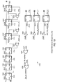
- FIG. 18 one embodiment of a schematic diagram of a frequency divider with a divisor range of 16-to-255 is shown.
- FIG. 18 utilizes the same design technique utilized in circuit 1100 (of FIG. 11A ) but extended to a divider with a divisor range of 16-to-255. In general, the same technique can be applied to various multi-octave divider ranges of interest.
- Divider circuit 1800 includes a series of four divide-by-2/3 cells (1802, 1804, 1806, and 1808) and three divide-by-1/2/3 cells (1812, 1816, and 1820).
- the effective range of possible divisor values 'N' may be determined by the formula 2 j ⁇ N ⁇ 2 (i+1) - 1, where 'j' represents the number of divide-by-2/3 cells and 'i' represents the total number of divide-by-2/3 cells and divide-by-1/2/3 cells.
- 'j' is four and 'i' is seven, so the effective range of possible divisor values is 16-to-255.
- circuit 1800 includes an additional series of two-input OR gates (1832 and 1830).
- the two highest P control signals (P7 and P6) corresponding to the two MSB's of the programming divisor word, may be coupled to the input nodes of the first two-input OR gate (1832) of the series.
- the output of OR gate 1832 may be coupled to an input node of the second two-input OR gate (1830) and to the D node of latch 1846; latch 1846 corresponds to the next to last divide-by-1/2/3 cell (1816) in the series of cells.
- the next or third MSB of the P control signals (P5) may be coupled to the other input node of the second OR gate 1830.
- OR gate 1830 may be coupled to the D node of latch 1850; latch 1850 corresponds to cell 1812.
- the arrangement of the additional series of two-input OR gates and coupling of corresponding signals may continue in a like fashion for the plurality of divide-by-1/2/3 cells and associated circuit elements.
- a latch, inverter gate, and two-input OR gate may be included in the frequency divider circuit.
- the Div1 node of each divide-by-1/2/3 cell may be coupled to a first input node of the two-input OR gate and to a Qb node of the latch.
- the mod out port of each divide-by-1/2/3 cell may be coupled to a second input node of the two-input OR gate and to an input node of the inverter gate.
- the output node of the inverter gate may be coupled to a clock port of the latch.
- the P control signal may be coupled to a D node of the corresponding latch if the series of cells includes only a single divide-by-1/2/3 cell.
- the signal coupled to the D node may come from the corresponding signal from the additional series of OR gates described above.
- the mod in port of each divide-by-1/2/3 cell may be coupled to an output node of the two-input OR gate corresponding to a subsequent divide-by-1/2/3 cell.
- the mod in port may be coupled to a high logic level (logic '1').
- Radio 1900 includes antenna 1905 for transmitting and receiving signals.
- Duplexer 1910 is coupled to antenna 1905, and duplexer 1910 is coupled to band-pass filter (BPF) 1915 on the receive path.
- Duplexer 1910 is also coupled to power amplifier (PA) 1985 on the transmit path of radio 1900.
- BPF 1915 is coupled to low-noise amplifier (LNA) 1920 on the receive path, and then LNA 1920 is coupled to demodulator 1925.
- Demodulator 1925 may be a quadrature demodulator or other type of demodulator.
- PLL 1930 may be employed as a local oscillator for demodulator 1925.
- PLL 1930 may include a crystal reference oscillator 1931, phase detector/charge pump/loop filter (PD/CP/LF) 1932, frequency divider 1933, and VCO 1934.
- Frequency divider 1933 may be a frequency divider with synchronous range extension, such as divider 1800 (of FIG. 18 ) or divider 1100 (of FIG. 11A ).
- Demodulator 1925 is coupled to baseband amplifier (BA) 1940, and (BA) 1940 is coupled to low-pass filter (LPF) 1945.
- LPF 1945 is coupled to analog-to-digital converter (ADC) 1950, and then ADC 1950 is coupled to baseband circuit 1955.
- Baseband circuit 1955 may receive and process the digital data received from ADC 1950 on the receive path.
- baseband circuit may generate digital data for transmission by radio 1900, and then convey the digital data to digital-to-analog converter (DAC) 1960.
- DAC 1960 is coupled to modulator 1965, and modulator 1965 may be a quadrature modulator or other type of modulator.
- PLL 1970 may be employed as a local oscillator for modulator 1965.
- PLL 1970 may include a crystal reference oscillator 1971, PD/CP/LF 1972, frequency divider 1973, and VCO 1974.
- Frequency divider 1973 may be a frequency divider with synchronous range extension, such as divider 1800 or divider 1100.
- the output of modulator 1965 is coupled to BPF 1980, and BPF 1980 is coupled to PA 1985.
- PA 1985 is coupled to duplexer 1910, and then duplexer 1910 may convey the transmit signal to antenna 1905.
- Radio 1900 depicts one embodiment of a radio or transceiver which may utilize a frequency divider as described in this specification.
- Other embodiments of radios may include other components not shown in FIG. 19 and/or omit certain of the components shown in FIG. 19 .
- Radio 1900 and frequency dividers 1933 and 1973 may be utilized in many types of radio applications, such as a multi-standard or multi-mode radio, a cognitive radio, or a software defined radio (SDR).
- the frequency dividers described in this specification may also be employed in frequency synthesizers or PLL's within many different types of products or applications, including cell phones, cordless phones, radar, electronic warfare systems, television, computers, cable modems, cable set-top boxes, and others.
- circuit 2000 may be incorporated in a radar 2010, cell phone 2020, radio 2030, or in various other devices or systems.
- Radio 2030 may be a multi-standard or multi-mode radio, cognitive radio, software defined radio (SDR), or other type of radio.
- the circuit 2000 includes at least one instance of frequency divider 1933.
- circuit 2000 may include functionality for any of various devices, such as fractional-N synthesizers, prescalers, multi-modulus dividers, PLLs, receivers, transmitters, transceivers, and other devices.
- circuit 2000 may include one or more of the components of radio 1900 shown in FIG. 19 .
Landscapes
- Engineering & Computer Science (AREA)
- Theoretical Computer Science (AREA)
- Physics & Mathematics (AREA)
- General Engineering & Computer Science (AREA)
- General Physics & Mathematics (AREA)
- Stabilization Of Oscillater, Synchronisation, Frequency Synthesizers (AREA)
Claims (13)
- Frequenzteiler aufweisend eine Reihe von einer oder mehreren geteilt-durch-2/3 Zellen und einer oder mehreren geteilt-durch-1/2/3 Zellen, wobei der Frequenzteiler ausgestaltet ist um eine Eingangsfrequenz durch einen Divisor auf aufeinanderfolgenden Ausgangszyklen zu teilen und wobei eine letzte geteilt-durch-1/2/3 Zelle der Reihe ausgestaltet ist um zwischen einem geteilt-durch-2 Modus und einem geteilt-durch-1 Modus überzugehen ansprechend auf Übergehen des Divisors über eine Oktavengrenze auf den aufeinanderfolgenden Ausgangszyklen.
- Frequenzteiler gemäß Anspruch 1, wobei der Frequenzteiler ausgestaltet ist um erweiterten Teilungsbereich, welcher sich über mehr als eine Oktave erstreckt, zu verwenden.
- Frequenzteiler gemäß Anspruch 1, wobei der Divisor von einer ersten positiven ganzen Zahl zu einer zweiten positiven ganzen Zahl über die Oktavengrenze übergeht.
- Frequenzteiler gemäß Anspruch 3, wobei das Übergehen über die Oktavengrenze Übergehen von einem Divisor gleich 2N - 1 zu einem Divisor gleich 2N oder Übergehen von einem Divisor gleich 2N zu einem Divisor gleich 2N - 1 umfasst, wobei N eine positive ganze Zahl ist.
- Frequenzteiler gemäß Anspruch 1, wobei die eine oder mehrere geteilt-durch-1/2/3 Zellen an einem Ende der Reihe sind.
- Frequenzteiler gemäß Anspruch 1, wobei zumindest eine geteilt-durch-1/2/3 Zelle ausgestaltet ist um in einen synchronen geteilt-durch-1 Modus einzutreten.
- Frequenzteiler gemäß Anspruch 6, wobei der Frequenzteiler weiterhin ausgestaltet ist um ein Steuerungsbit zu verwenden um die zumindest eine geteilt-durch-1/2/3 Zelle zu zwingen in den synchronen geteilt-durch-1 Modus einzutreten.
- Frequenzteiler gemäß Anspruch 1, wobei der Frequenzteiler weiterhin einen Latch, ein Inverter-Gatter, und ein Doppeleingang OR-Gatter aufweist, welche jeder geteilt-durch-1/2/3 Zelle entsprechen, wobei jede geteilt-durch-1/2/3 Zelle einen Div1 Port, einen modout Port und einen modin Port aufweist, und wobei jede geteilt-durch-1/2/3 Zelle ausgestaltet ist um:den Div1 Port an einen ersten Eingangsknoten des entsprechenden Doppeleingang OR-Gatters und einen Qb Knoten des entsprechenden Latches zu koppeln;den modout Port an einen zweiten Eingangsknoten des entsprechenden Doppeleingang OR-Gatters und an einen Eingangsknoten des entsprechenden Inverter-Gatters zu koppeln;einen Ausgangsknoten des entsprechenden Inverter-Gatters an einen Takt-Knoten des entsprechenden Latches zu koppeln;ein P Steuerungssignal an einen D Knoten des entsprechenden Latches zu koppeln; undden modin Port an einen Ausgangsknoten des Doppeleingang OR-Gatters, welches einer nachfolgenden Zelle in der Reihe entspricht, zu koppeln.
- Frequenzteiler gemäß Anspruch 8, wobei ein modin Port einer letzten geteilt-durch-1/2/3 Zelle in der Reihe an einen hohen Logikpegel gekoppelt ist.
- Frequenzteiler gemäß Anspruch 8, wobei der Frequenzteiler weiterhin aufweist:zwei oder mehr geteilt-durch-1/2/3 Zellen; undeine Vielzahl von zusammen kaskadierten Doppeleingang OR-Gattern;wobei für jedes Doppeleingang OR-Gatter der Vielzahl von Doppeleingang OR-Gattern, der Frequenzteiler ausgestaltet ist um:einen D Knoten eines entsprechenden Latches an einen Ausgangsknoten des Doppeleingang OR-Gatters zu koppeln;einen ersten Eingangsknoten des Doppeleingang OR-Gatters an ein P Steuerungssignal einer entsprechenden geteilt-durch-1/2/3 Zelle zu koppeln; undeinen zweiten Eingangsknoten des Doppeleingang OR-Gatters an ein P Steuerungssignal einer geteilt-durch-1/2/3 Zelle, welche der entsprechenden geteilt-durch-1/2/3 Zelle nachfolgt, zu koppeln.
- Frequenzteiler gemäß Anspruch 8, wobei ein effektiver Bereich von möglichen Divisor-Werten N durch eine Formel 2j≤N≤2(i+1) - 1 bestimmt ist, wobei j eine ganze Zahl ist, welche für eine Anzahl von geteilt-durch-2/3 Zellen steht und wobei i eine ganze Zahl ist, welche für eine Gesamtzahl von geteilt-durch-213 Zellen und geteilt-durch-1/2/3 Zellen steht.
- Frequenzteiler gemäß Anspruch 8, wobei der Frequenzteiler weiterhin ausgestaltet ist um ein Eingangs-Programmierwort zu empfangen, welches den Divisor-Wert spezifiziert.
- Schaltung gemäß Anspruch 6, wobei ein synchroner geteilt-durch-1 Modus Durchlaufen eines Eingangstakts in einem oder mehreren nicht verwendeten Latches umfasst.
Applications Claiming Priority (3)
| Application Number | Priority Date | Filing Date | Title |
|---|---|---|---|
| US201161437126P | 2011-01-28 | 2011-01-28 | |
| US13/356,995 US8552770B2 (en) | 2011-01-28 | 2012-01-24 | Frequency divider with synchronous range extension across octave boundaries |
| PCT/US2012/022364 WO2012103090A1 (en) | 2011-01-28 | 2012-01-24 | Frequency divider with synchronous range extension across octave boundaries |
Publications (2)
| Publication Number | Publication Date |
|---|---|
| EP2668723A1 EP2668723A1 (de) | 2013-12-04 |
| EP2668723B1 true EP2668723B1 (de) | 2014-11-26 |
Family
ID=46576842
Family Applications (1)
| Application Number | Title | Priority Date | Filing Date |
|---|---|---|---|
| EP12703652.3A Active EP2668723B1 (de) | 2011-01-28 | 2012-01-24 | Frequenzteiler mit synchroner bereichserweiterung über oktavengrenzen |
Country Status (5)
| Country | Link |
|---|---|
| US (1) | US8552770B2 (de) |
| EP (1) | EP2668723B1 (de) |
| JP (1) | JP5837617B2 (de) |
| CN (1) | CN103229420B (de) |
| WO (1) | WO2012103090A1 (de) |
Families Citing this family (20)
| Publication number | Priority date | Publication date | Assignee | Title |
|---|---|---|---|---|
| TWI463799B (zh) * | 2011-07-29 | 2014-12-01 | Mstar Semiconductor Inc | 多模數除頻器以及相關之控制方法 |
| US8891725B2 (en) * | 2012-07-02 | 2014-11-18 | Qualcomm Incorporated | Frequency divider with improved linearity for a fractional-N synthesizer using a multi-modulus prescaler |
| US8963599B2 (en) | 2012-12-13 | 2015-02-24 | Coherent Logix, Incorporated | Multi-frequency clock skew control for inter-chip communication in synchronous digital systems |
| US9018988B2 (en) * | 2013-04-18 | 2015-04-28 | MEMS Vision LLC | Methods and architectures for extended range arbitrary ratio dividers |
| US9118333B1 (en) * | 2013-08-29 | 2015-08-25 | Integrated Device Technology Inc. | Self-adaptive multi-modulus dividers containing div2/3 cells therein |
| US8917122B1 (en) * | 2013-09-06 | 2014-12-23 | Infinion Technologies AG | Frequency dividers |
| US9397667B2 (en) | 2014-09-04 | 2016-07-19 | Texas Instruments Deutschland Gmbh | Shared divide by N clock divider |
| CN105471427B (zh) | 2014-09-04 | 2019-07-26 | 中芯国际集成电路制造(上海)有限公司 | 一种多模分频器和电子装置 |
| US9306574B1 (en) * | 2015-03-04 | 2016-04-05 | Apple Inc. | Clock divider circuit with synchronized switching |
| US9900012B2 (en) | 2015-04-16 | 2018-02-20 | Bae Systems Information And Electronic Systems Integration Inc. | Multi-modulus divider with power-of-2 boundary condition support |
| US9438257B1 (en) * | 2015-07-02 | 2016-09-06 | Aura Semiconductor Pvt. Ltd | Programmable frequency divider providing output with reduced duty-cycle variations over a range of divide ratios |
| US9577646B1 (en) * | 2015-08-07 | 2017-02-21 | Qualcomm Incorporated | Fractional phase locked loop (PLL) architecture |
| JP6437142B2 (ja) * | 2016-03-16 | 2018-12-12 | 三菱電機株式会社 | 可変分周器 |
| CN107547082B (zh) * | 2016-06-23 | 2023-10-13 | 豪威科技股份有限公司 | 用于数字系统中时钟合成器的1-16和1.5-7.5分频器 |
| US10523211B2 (en) | 2016-08-17 | 2019-12-31 | Silicon Laboratories Inc. | Wide range glitchless switchable clock divider with modified 2/3 divider stages |
| US10230381B2 (en) * | 2017-05-04 | 2019-03-12 | Cavium, Llc | Frequency divider |
| US10700669B2 (en) | 2018-06-19 | 2020-06-30 | Aura Semiconductor Pvt. Ltd | Avoiding very low duty cycles in a divided clock generated by a frequency divider |
| RU197065U1 (ru) * | 2019-12-12 | 2020-03-27 | Евгений Борисович Колесников | Делитель частоты гармонического сигнала |
| RU206322U1 (ru) * | 2021-05-24 | 2021-09-06 | Евгений Борисович Колесников | Делитель частоты гармонического сигнала |
| RU206323U1 (ru) * | 2021-05-24 | 2021-09-06 | Евгений Борисович Колесников | Делитель частоты гармонического сигнала |
Family Cites Families (8)
| Publication number | Priority date | Publication date | Assignee | Title |
|---|---|---|---|---|
| FR2719728A1 (fr) * | 1994-05-04 | 1995-11-10 | Philips Composants | Diviseur de fréquence, synthétiseur de fréquence comportant un tel diviseur et radiotéléphone comportant un tel synthétiseur. |
| EP0872959B1 (de) * | 1997-04-15 | 2003-12-10 | Koninklijke Philips Electronics N.V. | Rauscharmer Frequenzteiler |
| US5948046A (en) * | 1997-12-15 | 1999-09-07 | Telefonaktiebolaget Lm Ericsson | Multi-divide frequency division |
| US6959063B1 (en) * | 2000-02-29 | 2005-10-25 | Telefonaktiebolaget L M Ericsson (Publ) | Fractional-N phase locked loop |
| DE10251703B4 (de) | 2002-11-06 | 2005-08-04 | Infineon Technologies Ag | Schaltungsanordnung zur Frequenzteilung und Phasenregelschleife mit der Schaltungsanordnung |
| TWI222786B (en) * | 2003-09-17 | 2004-10-21 | Mediatek Inc | Multi-modulus programmable frequency divider |
| DE102005030356B4 (de) * | 2005-06-29 | 2011-07-07 | Infineon Technologies AG, 81669 | Digitaler Phasenregelkreis und Verfahren zur Regelung eines digitalen Phasenregelkreises |
| CN101465645B (zh) * | 2007-12-19 | 2010-12-15 | 中国科学院微电子研究所 | 一种小数/整数分频器 |
-
2012
- 2012-01-24 CN CN201280003904.9A patent/CN103229420B/zh active Active
- 2012-01-24 JP JP2013551286A patent/JP5837617B2/ja active Active
- 2012-01-24 WO PCT/US2012/022364 patent/WO2012103090A1/en not_active Ceased
- 2012-01-24 US US13/356,995 patent/US8552770B2/en active Active
- 2012-01-24 EP EP12703652.3A patent/EP2668723B1/de active Active
Also Published As
| Publication number | Publication date |
|---|---|
| CN103229420B (zh) | 2016-09-28 |
| US8552770B2 (en) | 2013-10-08 |
| US20120194220A1 (en) | 2012-08-02 |
| WO2012103090A1 (en) | 2012-08-02 |
| JP5837617B2 (ja) | 2015-12-24 |
| EP2668723A1 (de) | 2013-12-04 |
| JP2014510439A (ja) | 2014-04-24 |
| CN103229420A (zh) | 2013-07-31 |
Similar Documents
| Publication | Publication Date | Title |
|---|---|---|
| US8552770B2 (en) | Frequency divider with synchronous range extension across octave boundaries | |
| CN101371444B (zh) | 用于多模移动通信设备的可配置多模数分频器及其相关方法 | |
| KR101611814B1 (ko) | 분수 분주형 주파수 합성기의 광범위 멀티-모듈러스 분할기 | |
| CN101496284B (zh) | 多模除法器重定时电路 | |
| US9018988B2 (en) | Methods and architectures for extended range arbitrary ratio dividers | |
| US9900012B2 (en) | Multi-modulus divider with power-of-2 boundary condition support | |
| US9843334B2 (en) | Frequency synthesizer | |
| US8466720B2 (en) | Frequency division of an input clock signal | |
| CN1864333B (zh) | 相位切换双模除频器及包括该除频器的频率合成器 | |
| Ergintav et al. | Low-power and low-noise programmable frequency dividers in a 130 nm SiGe BiCMOS technology | |
| US7653168B2 (en) | Digital clock dividing circuit | |
| JPH0548433A (ja) | 多段分周器 | |
| Wang et al. | A generic multi-modulus divider architecture for fractional-N frequency synthesisers | |
| KR101091488B1 (ko) | 프리스케일러 및 이를 구비한 위상고정루프 주파수 합성기 | |
| Xiangning et al. | A Low Voltage Delta-Sigma Fractional Frequency Divider for Multi-band WSN Frequency Synthesizers | |
| JP2003324345A (ja) | 分周器、分周回路及びpll回路 | |
| HK1133960A (en) | Multi-modulus divider retiming circuit |
Legal Events
| Date | Code | Title | Description |
|---|---|---|---|
| PUAI | Public reference made under article 153(3) epc to a published international application that has entered the european phase |
Free format text: ORIGINAL CODE: 0009012 |
|
| 17P | Request for examination filed |
Effective date: 20130711 |
|
| AK | Designated contracting states |
Kind code of ref document: A1 Designated state(s): AL AT BE BG CH CY CZ DE DK EE ES FI FR GB GR HR HU IE IS IT LI LT LU LV MC MK MT NL NO PL PT RO RS SE SI SK SM TR |
|
| DAX | Request for extension of the european patent (deleted) | ||
| GRAP | Despatch of communication of intention to grant a patent |
Free format text: ORIGINAL CODE: EPIDOSNIGR1 |
|
| INTG | Intention to grant announced |
Effective date: 20140611 |
|
| GRAS | Grant fee paid |
Free format text: ORIGINAL CODE: EPIDOSNIGR3 |
|
| GRAA | (expected) grant |
Free format text: ORIGINAL CODE: 0009210 |
|
| AK | Designated contracting states |
Kind code of ref document: B1 Designated state(s): AL AT BE BG CH CY CZ DE DK EE ES FI FR GB GR HR HU IE IS IT LI LT LU LV MC MK MT NL NO PL PT RO RS SE SI SK SM TR |
|
| REG | Reference to a national code |
Ref country code: GB Ref legal event code: FG4D |
|
| REG | Reference to a national code |
Ref country code: CH Ref legal event code: EP |
|
| REG | Reference to a national code |
Ref country code: AT Ref legal event code: REF Ref document number: 698686 Country of ref document: AT Kind code of ref document: T Effective date: 20141215 |
|
| REG | Reference to a national code |
Ref country code: IE Ref legal event code: FG4D |
|
| REG | Reference to a national code |
Ref country code: DE Ref legal event code: R096 Ref document number: 602012003992 Country of ref document: DE Effective date: 20150108 |
|
| REG | Reference to a national code |
Ref country code: NL Ref legal event code: VDEP Effective date: 20141126 |
|
| REG | Reference to a national code |
Ref country code: AT Ref legal event code: MK05 Ref document number: 698686 Country of ref document: AT Kind code of ref document: T Effective date: 20141126 |
|
| REG | Reference to a national code |
Ref country code: LT Ref legal event code: MG4D |
|
| PG25 | Lapsed in a contracting state [announced via postgrant information from national office to epo] |
Ref country code: LT Free format text: LAPSE BECAUSE OF FAILURE TO SUBMIT A TRANSLATION OF THE DESCRIPTION OR TO PAY THE FEE WITHIN THE PRESCRIBED TIME-LIMIT Effective date: 20141126 Ref country code: FI Free format text: LAPSE BECAUSE OF FAILURE TO SUBMIT A TRANSLATION OF THE DESCRIPTION OR TO PAY THE FEE WITHIN THE PRESCRIBED TIME-LIMIT Effective date: 20141126 Ref country code: ES Free format text: LAPSE BECAUSE OF FAILURE TO SUBMIT A TRANSLATION OF THE DESCRIPTION OR TO PAY THE FEE WITHIN THE PRESCRIBED TIME-LIMIT Effective date: 20141126 Ref country code: IS Free format text: LAPSE BECAUSE OF FAILURE TO SUBMIT A TRANSLATION OF THE DESCRIPTION OR TO PAY THE FEE WITHIN THE PRESCRIBED TIME-LIMIT Effective date: 20150326 Ref country code: PT Free format text: LAPSE BECAUSE OF FAILURE TO SUBMIT A TRANSLATION OF THE DESCRIPTION OR TO PAY THE FEE WITHIN THE PRESCRIBED TIME-LIMIT Effective date: 20150326 Ref country code: NL Free format text: LAPSE BECAUSE OF FAILURE TO SUBMIT A TRANSLATION OF THE DESCRIPTION OR TO PAY THE FEE WITHIN THE PRESCRIBED TIME-LIMIT Effective date: 20141126 Ref country code: NO Free format text: LAPSE BECAUSE OF FAILURE TO SUBMIT A TRANSLATION OF THE DESCRIPTION OR TO PAY THE FEE WITHIN THE PRESCRIBED TIME-LIMIT Effective date: 20150226 |
|
| PG25 | Lapsed in a contracting state [announced via postgrant information from national office to epo] |
Ref country code: SE Free format text: LAPSE BECAUSE OF FAILURE TO SUBMIT A TRANSLATION OF THE DESCRIPTION OR TO PAY THE FEE WITHIN THE PRESCRIBED TIME-LIMIT Effective date: 20141126 Ref country code: GR Free format text: LAPSE BECAUSE OF FAILURE TO SUBMIT A TRANSLATION OF THE DESCRIPTION OR TO PAY THE FEE WITHIN THE PRESCRIBED TIME-LIMIT Effective date: 20150227 Ref country code: LV Free format text: LAPSE BECAUSE OF FAILURE TO SUBMIT A TRANSLATION OF THE DESCRIPTION OR TO PAY THE FEE WITHIN THE PRESCRIBED TIME-LIMIT Effective date: 20141126 Ref country code: AT Free format text: LAPSE BECAUSE OF FAILURE TO SUBMIT A TRANSLATION OF THE DESCRIPTION OR TO PAY THE FEE WITHIN THE PRESCRIBED TIME-LIMIT Effective date: 20141126 Ref country code: RS Free format text: LAPSE BECAUSE OF FAILURE TO SUBMIT A TRANSLATION OF THE DESCRIPTION OR TO PAY THE FEE WITHIN THE PRESCRIBED TIME-LIMIT Effective date: 20141126 Ref country code: HR Free format text: LAPSE BECAUSE OF FAILURE TO SUBMIT A TRANSLATION OF THE DESCRIPTION OR TO PAY THE FEE WITHIN THE PRESCRIBED TIME-LIMIT Effective date: 20141126 Ref country code: CY Free format text: LAPSE BECAUSE OF FAILURE TO SUBMIT A TRANSLATION OF THE DESCRIPTION OR TO PAY THE FEE WITHIN THE PRESCRIBED TIME-LIMIT Effective date: 20141126 |
|
| PG25 | Lapsed in a contracting state [announced via postgrant information from national office to epo] |
Ref country code: RO Free format text: LAPSE BECAUSE OF FAILURE TO SUBMIT A TRANSLATION OF THE DESCRIPTION OR TO PAY THE FEE WITHIN THE PRESCRIBED TIME-LIMIT Effective date: 20141126 Ref country code: SK Free format text: LAPSE BECAUSE OF FAILURE TO SUBMIT A TRANSLATION OF THE DESCRIPTION OR TO PAY THE FEE WITHIN THE PRESCRIBED TIME-LIMIT Effective date: 20141126 Ref country code: DK Free format text: LAPSE BECAUSE OF FAILURE TO SUBMIT A TRANSLATION OF THE DESCRIPTION OR TO PAY THE FEE WITHIN THE PRESCRIBED TIME-LIMIT Effective date: 20141126 Ref country code: EE Free format text: LAPSE BECAUSE OF FAILURE TO SUBMIT A TRANSLATION OF THE DESCRIPTION OR TO PAY THE FEE WITHIN THE PRESCRIBED TIME-LIMIT Effective date: 20141126 Ref country code: CZ Free format text: LAPSE BECAUSE OF FAILURE TO SUBMIT A TRANSLATION OF THE DESCRIPTION OR TO PAY THE FEE WITHIN THE PRESCRIBED TIME-LIMIT Effective date: 20141126 |
|
| REG | Reference to a national code |
Ref country code: DE Ref legal event code: R097 Ref document number: 602012003992 Country of ref document: DE |
|
| REG | Reference to a national code |
Ref country code: CH Ref legal event code: PL |
|
| PG25 | Lapsed in a contracting state [announced via postgrant information from national office to epo] |
Ref country code: PL Free format text: LAPSE BECAUSE OF FAILURE TO SUBMIT A TRANSLATION OF THE DESCRIPTION OR TO PAY THE FEE WITHIN THE PRESCRIBED TIME-LIMIT Effective date: 20141126 Ref country code: LU Free format text: LAPSE BECAUSE OF FAILURE TO SUBMIT A TRANSLATION OF THE DESCRIPTION OR TO PAY THE FEE WITHIN THE PRESCRIBED TIME-LIMIT Effective date: 20150124 |
|
| PG25 | Lapsed in a contracting state [announced via postgrant information from national office to epo] |
Ref country code: MC Free format text: LAPSE BECAUSE OF FAILURE TO SUBMIT A TRANSLATION OF THE DESCRIPTION OR TO PAY THE FEE WITHIN THE PRESCRIBED TIME-LIMIT Effective date: 20141126 |
|
| PLBE | No opposition filed within time limit |
Free format text: ORIGINAL CODE: 0009261 |
|
| STAA | Information on the status of an ep patent application or granted ep patent |
Free format text: STATUS: NO OPPOSITION FILED WITHIN TIME LIMIT |
|
| PG25 | Lapsed in a contracting state [announced via postgrant information from national office to epo] |
Ref country code: LI Free format text: LAPSE BECAUSE OF NON-PAYMENT OF DUE FEES Effective date: 20150131 Ref country code: CH Free format text: LAPSE BECAUSE OF NON-PAYMENT OF DUE FEES Effective date: 20150131 |
|
| 26N | No opposition filed |
Effective date: 20150827 |
|
| REG | Reference to a national code |
Ref country code: IE Ref legal event code: MM4A |
|
| PG25 | Lapsed in a contracting state [announced via postgrant information from national office to epo] |
Ref country code: IT Free format text: LAPSE BECAUSE OF FAILURE TO SUBMIT A TRANSLATION OF THE DESCRIPTION OR TO PAY THE FEE WITHIN THE PRESCRIBED TIME-LIMIT Effective date: 20141126 |
|
| REG | Reference to a national code |
Ref country code: FR Ref legal event code: PLFP Year of fee payment: 5 |
|
| PG25 | Lapsed in a contracting state [announced via postgrant information from national office to epo] |
Ref country code: IE Free format text: LAPSE BECAUSE OF NON-PAYMENT OF DUE FEES Effective date: 20150124 |
|
| PG25 | Lapsed in a contracting state [announced via postgrant information from national office to epo] |
Ref country code: SI Free format text: LAPSE BECAUSE OF FAILURE TO SUBMIT A TRANSLATION OF THE DESCRIPTION OR TO PAY THE FEE WITHIN THE PRESCRIBED TIME-LIMIT Effective date: 20141126 |
|
| PG25 | Lapsed in a contracting state [announced via postgrant information from national office to epo] |
Ref country code: MT Free format text: LAPSE BECAUSE OF FAILURE TO SUBMIT A TRANSLATION OF THE DESCRIPTION OR TO PAY THE FEE WITHIN THE PRESCRIBED TIME-LIMIT Effective date: 20141126 |
|
| REG | Reference to a national code |
Ref country code: FR Ref legal event code: PLFP Year of fee payment: 6 |
|
| PG25 | Lapsed in a contracting state [announced via postgrant information from national office to epo] |
Ref country code: HU Free format text: LAPSE BECAUSE OF FAILURE TO SUBMIT A TRANSLATION OF THE DESCRIPTION OR TO PAY THE FEE WITHIN THE PRESCRIBED TIME-LIMIT; INVALID AB INITIO Effective date: 20120124 Ref country code: SM Free format text: LAPSE BECAUSE OF FAILURE TO SUBMIT A TRANSLATION OF THE DESCRIPTION OR TO PAY THE FEE WITHIN THE PRESCRIBED TIME-LIMIT Effective date: 20141126 Ref country code: BG Free format text: LAPSE BECAUSE OF FAILURE TO SUBMIT A TRANSLATION OF THE DESCRIPTION OR TO PAY THE FEE WITHIN THE PRESCRIBED TIME-LIMIT Effective date: 20141126 |
|
| PG25 | Lapsed in a contracting state [announced via postgrant information from national office to epo] |
Ref country code: BE Free format text: LAPSE BECAUSE OF NON-PAYMENT OF DUE FEES Effective date: 20150131 |
|
| PG25 | Lapsed in a contracting state [announced via postgrant information from national office to epo] |
Ref country code: TR Free format text: LAPSE BECAUSE OF FAILURE TO SUBMIT A TRANSLATION OF THE DESCRIPTION OR TO PAY THE FEE WITHIN THE PRESCRIBED TIME-LIMIT Effective date: 20141126 |
|
| REG | Reference to a national code |
Ref country code: FR Ref legal event code: PLFP Year of fee payment: 7 |
|
| PG25 | Lapsed in a contracting state [announced via postgrant information from national office to epo] |
Ref country code: MK Free format text: LAPSE BECAUSE OF FAILURE TO SUBMIT A TRANSLATION OF THE DESCRIPTION OR TO PAY THE FEE WITHIN THE PRESCRIBED TIME-LIMIT Effective date: 20141126 |
|
| PG25 | Lapsed in a contracting state [announced via postgrant information from national office to epo] |
Ref country code: AL Free format text: LAPSE BECAUSE OF FAILURE TO SUBMIT A TRANSLATION OF THE DESCRIPTION OR TO PAY THE FEE WITHIN THE PRESCRIBED TIME-LIMIT Effective date: 20141126 |
|
| REG | Reference to a national code |
Ref country code: GB Ref legal event code: 732E Free format text: REGISTERED BETWEEN 20251120 AND 20251126 |
|
| REG | Reference to a national code |
Ref country code: DE Ref legal event code: R081 Ref document number: 602012003992 Country of ref document: DE Owner name: HYPERX HOLDINGS LLC, AUSTIN, US Free format text: FORMER OWNER: COHERENT LOGIX INC., AUSTIN, TEX., US |
|
| PGFP | Annual fee paid to national office [announced via postgrant information from national office to epo] |
Ref country code: GB Payment date: 20260127 Year of fee payment: 15 |
|
| PGFP | Annual fee paid to national office [announced via postgrant information from national office to epo] |
Ref country code: DE Payment date: 20260128 Year of fee payment: 15 |
|
| PGFP | Annual fee paid to national office [announced via postgrant information from national office to epo] |
Ref country code: FR Payment date: 20260126 Year of fee payment: 15 |