EP2669957A2 - Cellule solaire et procédé de fabrication de cette dernière - Google Patents
Cellule solaire et procédé de fabrication de cette dernière Download PDFInfo
- Publication number
- EP2669957A2 EP2669957A2 EP12739255.3A EP12739255A EP2669957A2 EP 2669957 A2 EP2669957 A2 EP 2669957A2 EP 12739255 A EP12739255 A EP 12739255A EP 2669957 A2 EP2669957 A2 EP 2669957A2
- Authority
- EP
- European Patent Office
- Prior art keywords
- barrier layer
- layer
- substrate
- solar cell
- electrode layer
- Prior art date
- Legal status (The legal status is an assumption and is not a legal conclusion. Google has not performed a legal analysis and makes no representation as to the accuracy of the status listed.)
- Withdrawn
Links
Images


Classifications
-
- H—ELECTRICITY
- H10—SEMICONDUCTOR DEVICES; ELECTRIC SOLID-STATE DEVICES NOT OTHERWISE PROVIDED FOR
- H10F—INORGANIC SEMICONDUCTOR DEVICES SENSITIVE TO INFRARED RADIATION, LIGHT, ELECTROMAGNETIC RADIATION OF SHORTER WAVELENGTH OR CORPUSCULAR RADIATION
- H10F77/00—Constructional details of devices covered by this subclass
- H10F77/20—Electrodes
- H10F77/206—Electrodes for devices having potential barriers
- H10F77/211—Electrodes for devices having potential barriers for photovoltaic cells
-
- H—ELECTRICITY
- H10—SEMICONDUCTOR DEVICES; ELECTRIC SOLID-STATE DEVICES NOT OTHERWISE PROVIDED FOR
- H10F—INORGANIC SEMICONDUCTOR DEVICES SENSITIVE TO INFRARED RADIATION, LIGHT, ELECTROMAGNETIC RADIATION OF SHORTER WAVELENGTH OR CORPUSCULAR RADIATION
- H10F10/00—Individual photovoltaic cells, e.g. solar cells
-
- H—ELECTRICITY
- H10—SEMICONDUCTOR DEVICES; ELECTRIC SOLID-STATE DEVICES NOT OTHERWISE PROVIDED FOR
- H10F—INORGANIC SEMICONDUCTOR DEVICES SENSITIVE TO INFRARED RADIATION, LIGHT, ELECTROMAGNETIC RADIATION OF SHORTER WAVELENGTH OR CORPUSCULAR RADIATION
- H10F10/00—Individual photovoltaic cells, e.g. solar cells
- H10F10/10—Individual photovoltaic cells, e.g. solar cells having potential barriers
- H10F10/16—Photovoltaic cells having only PN heterojunction potential barriers
- H10F10/167—Photovoltaic cells having only PN heterojunction potential barriers comprising Group I-III-VI materials, e.g. CdS/CuInSe2 [CIS] heterojunction photovoltaic cells
-
- H—ELECTRICITY
- H10—SEMICONDUCTOR DEVICES; ELECTRIC SOLID-STATE DEVICES NOT OTHERWISE PROVIDED FOR
- H10F—INORGANIC SEMICONDUCTOR DEVICES SENSITIVE TO INFRARED RADIATION, LIGHT, ELECTROMAGNETIC RADIATION OF SHORTER WAVELENGTH OR CORPUSCULAR RADIATION
- H10F77/00—Constructional details of devices covered by this subclass
- H10F77/10—Semiconductor bodies
- H10F77/16—Material structures, e.g. crystalline structures, film structures or crystal plane orientations
- H10F77/169—Thin semiconductor films on metallic or insulating substrates
- H10F77/1694—Thin semiconductor films on metallic or insulating substrates the films including Group I-III-VI materials, e.g. CIS or CIGS
-
- H—ELECTRICITY
- H10—SEMICONDUCTOR DEVICES; ELECTRIC SOLID-STATE DEVICES NOT OTHERWISE PROVIDED FOR
- H10F—INORGANIC SEMICONDUCTOR DEVICES SENSITIVE TO INFRARED RADIATION, LIGHT, ELECTROMAGNETIC RADIATION OF SHORTER WAVELENGTH OR CORPUSCULAR RADIATION
- H10F77/00—Constructional details of devices covered by this subclass
- H10F77/20—Electrodes
- H10F77/244—Electrodes made of transparent conductive layers, e.g. transparent conductive oxide [TCO] layers
- H10F77/251—Electrodes made of transparent conductive layers, e.g. transparent conductive oxide [TCO] layers comprising zinc oxide [ZnO]
-
- H—ELECTRICITY
- H10—SEMICONDUCTOR DEVICES; ELECTRIC SOLID-STATE DEVICES NOT OTHERWISE PROVIDED FOR
- H10P—GENERIC PROCESSES OR APPARATUS FOR THE MANUFACTURE OR TREATMENT OF DEVICES COVERED BY CLASS H10
- H10P14/00—Formation of materials, e.g. in the shape of layers or pillars
- H10P14/20—Formation of materials, e.g. in the shape of layers or pillars of semiconductor materials
- H10P14/29—Formation of materials, e.g. in the shape of layers or pillars of semiconductor materials characterised by the substrates
- H10P14/2901—Materials
- H10P14/2923—Materials being conductive materials, e.g. metallic silicides
-
- H—ELECTRICITY
- H10—SEMICONDUCTOR DEVICES; ELECTRIC SOLID-STATE DEVICES NOT OTHERWISE PROVIDED FOR
- H10P—GENERIC PROCESSES OR APPARATUS FOR THE MANUFACTURE OR TREATMENT OF DEVICES COVERED BY CLASS H10
- H10P14/00—Formation of materials, e.g. in the shape of layers or pillars
- H10P14/20—Formation of materials, e.g. in the shape of layers or pillars of semiconductor materials
- H10P14/32—Formation of materials, e.g. in the shape of layers or pillars of semiconductor materials characterised by intermediate layers between substrates and deposited layers
- H10P14/3202—Materials thereof
-
- H—ELECTRICITY
- H10—SEMICONDUCTOR DEVICES; ELECTRIC SOLID-STATE DEVICES NOT OTHERWISE PROVIDED FOR
- H10P—GENERIC PROCESSES OR APPARATUS FOR THE MANUFACTURE OR TREATMENT OF DEVICES COVERED BY CLASS H10
- H10P14/00—Formation of materials, e.g. in the shape of layers or pillars
- H10P14/20—Formation of materials, e.g. in the shape of layers or pillars of semiconductor materials
- H10P14/32—Formation of materials, e.g. in the shape of layers or pillars of semiconductor materials characterised by intermediate layers between substrates and deposited layers
- H10P14/3202—Materials thereof
- H10P14/3224—Materials thereof being Group IIB-VIA semiconductors
- H10P14/3226—Oxides
-
- H—ELECTRICITY
- H10—SEMICONDUCTOR DEVICES; ELECTRIC SOLID-STATE DEVICES NOT OTHERWISE PROVIDED FOR
- H10P—GENERIC PROCESSES OR APPARATUS FOR THE MANUFACTURE OR TREATMENT OF DEVICES COVERED BY CLASS H10
- H10P14/00—Formation of materials, e.g. in the shape of layers or pillars
- H10P14/20—Formation of materials, e.g. in the shape of layers or pillars of semiconductor materials
- H10P14/32—Formation of materials, e.g. in the shape of layers or pillars of semiconductor materials characterised by intermediate layers between substrates and deposited layers
- H10P14/3242—Structure
- H10P14/3244—Layer structure
- H10P14/3251—Layer structure consisting of three or more layers
-
- H—ELECTRICITY
- H10—SEMICONDUCTOR DEVICES; ELECTRIC SOLID-STATE DEVICES NOT OTHERWISE PROVIDED FOR
- H10P—GENERIC PROCESSES OR APPARATUS FOR THE MANUFACTURE OR TREATMENT OF DEVICES COVERED BY CLASS H10
- H10P14/00—Formation of materials, e.g. in the shape of layers or pillars
- H10P14/20—Formation of materials, e.g. in the shape of layers or pillars of semiconductor materials
- H10P14/34—Deposited materials, e.g. layers
- H10P14/3402—Deposited materials, e.g. layers characterised by the chemical composition
- H10P14/3436—Deposited materials, e.g. layers characterised by the chemical composition being chalcogenide semiconductor materials not being oxides, e.g. ternary compounds
-
- Y—GENERAL TAGGING OF NEW TECHNOLOGICAL DEVELOPMENTS; GENERAL TAGGING OF CROSS-SECTIONAL TECHNOLOGIES SPANNING OVER SEVERAL SECTIONS OF THE IPC; TECHNICAL SUBJECTS COVERED BY FORMER USPC CROSS-REFERENCE ART COLLECTIONS [XRACs] AND DIGESTS
- Y02—TECHNOLOGIES OR APPLICATIONS FOR MITIGATION OR ADAPTATION AGAINST CLIMATE CHANGE
- Y02E—REDUCTION OF GREENHOUSE GAS [GHG] EMISSIONS, RELATED TO ENERGY GENERATION, TRANSMISSION OR DISTRIBUTION
- Y02E10/00—Energy generation through renewable energy sources
- Y02E10/50—Photovoltaic [PV] energy
- Y02E10/541—CuInSe2 material PV cells
Definitions
- the embodiment relates to a solar cell and a method for manufacturing the same.
- a solar cell converts solar energy into electrical energy. Recently, as energy consumption is increased, the solar cell has been extensively used commercially.
- a solar cell according to the related art is formed by forming a semiconductor layer on a transparent substrate.
- a metal substrate, a glass substrate, or a plastic substrate is used as the transparent substrate.
- the embodiment provides a solar cell capable of preventing the efficiency from being deteriorated due to a metal component contained in a substrate and a method for manufacturing the same.
- a solar cell including: a substrate; a back electrode layer, a light absorbing layer, and a transparent electrode layer sequentially formed on the substrate; and a barrier layer formed between the substrate and the back electrode layer and including a group II element.
- a method for manufacturing a solar cell including: preparing a metal substrate; forming a barrier layer including a group II element on the metal substrate; and sequentially forming a back electrode layer, a light absorbing layer, and a transparent electrode layer on the barrier layer.
- a barrier layer for preventing diffusion of a metal is formed on the substrate, so that the efficiency of the solar cell can be prevented from being deteriorated due to a metal component contained in the substrate.
- the barrier layer contains a sodium (Na) component so that the efficiency of the solar cell can be improved due to diffusion of the Na component.
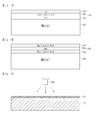
- FIG. 1 is a sectional view showing a solar cell on which a barrier layer is formed according to an embodiment of the invention
- FIG. 2 is sectional view showing the barrier layer according to the embodiment of the invention.
- FIGS. 3 to 6 are sectional views showing modified examples of a barrier layer according to the embodiment of the invention.
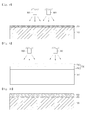
- FIGS. 7 to 12 are sectional views showing a method of manufacturing a solar cell according to an embodiment of the invention.
- FIG. 1 is a sectional view showing a solar cell on which a barrier layer is formed according to an embodiment of the invention
- FIG. 2 is sectional view showing the barrier layer according to the embodiment of the invention
- FIGS. 3 to 6 are sectional views showing modified examples of a barrier layer according to the embodiment of the invention.
- the solar cell according to the embodiment includes a substrate 100 as well as a back electrode layer 200, a light absorbing layer 300, and a transparent electrode layer 600 which are sequentially formed on the substrate 100, and a barrier layer 700 formed between the substrate 100 and the back electrode layer 200 to prevent diffusion of a metal component contained in the substrate 100.
- a first buffer 400 and a second buffer layer 500 may be further formed on the light absorbing layer 300.
- the substrate 100 has a rectangular plate shape and may include a transparent material.
- a metal substrate containing a metal component may be used as the substrate 100 according to the embodiment.
- the back electrode layer 200 is formed on the substrate 100.
- the back electrode layer 200 serves as an n-type electrode, and may include molybdenum (Mo).
- the back electrode layer 200 may include at least one of aluminum (Al), nickel (Ni), chromium (Cr), titanium (Ti), silver (Ag), and gold (Au) being a conductive material in addition to the Mo.
- the back electrode layer 200 may be formed to provide at least two layers using homogeneous or heterogeneous metal.
- the light absorbing layer 300 is formed on the back electrode layer 200.
- the light absorbing layer 300 may have a group I-III-VI compound.
- the light absorbing layer 300 may include at least one of CIGS, CIGSS, CZTS, CIS, CGS, and CdTe.
- the light absorbing layer 300 may include at least one material selected from the group consisting of CdTe, CuInSe 2 , Cu(In,Ga)Se 2 , Cu(In,Ga)(Se,S) 2 , Ag(InGa)Se 2 , Cu(In,Al)Se 2 , and CuGaSe 2 .
- a first buffer layer 400 and a second buffer layer 500 may be sequentially formed on the light absorbing layer 300.
- the first buffer layer 400 may be formed by using a material including cadmium sulfide (CdS).
- the first buffer layer 400 may include a material such as CdSe, ZnS, ZnSe, or ZnMgxOy in addition to the CdS.
- the first buffer layer 400 may have an energy bandgap in the range of about 1.9 eV to about 2.3 eV corresponding to the intermediate energy bandgap between the back electrode layer 200 and the transparent electrode layer 600.
- the first buffer layer 400 may include at least two layers.
- the second buffer layer 500 is formed of ZnO to have a high resistance.
- the second buffer layer 500 may insulate the transparent electrode layer 600 to be described later and prevent shock damage.
- the second buffer 500 may be omitted according to a type of the first buffer 400.
- the transparent electrode layer 600 is formed on the second buffer layer 500.
- the transparent electrode layer 600 includes a transparent conductive material, or may include aluminum doped zinc oxide (AZO; ZnO:Al).
- the transparent electrode layer 600 may be formed by using GZO, BZO, FTO, or ITO as well as the AZO.
- a material of the transparent electrode layer 600 is not limited to the above-mentioned material. That is, the transparent electrode layer 600 may be formed by using one of zinc oxide (ZnO), tin oxide (SnO 2 ), and indium tin oxide (ITO), each of which has high light transmittance and electric conductivity.
- ZnO zinc oxide
- SnO 2 tin oxide
- ITO indium tin oxide
- the barrier layer 700 according to the embodiment is formed between the substrate 100 and the back electrode layer 200. In other words, the barrier layer 700 is formed on the substrate 100.
- the barrier layer 700 serves to prevent a metal component contained in the substrate 100 from moving into a semiconductor layer of the solar cell.
- the barrier layer 700 may include ZnO and may be formed on the substrate 100 to have a predetermined thickness in a range of, for example, 50 nm to 1 ⁇ m.
- Al 2 O 3 , SiO 2 , and Cr may be used as the barrier layer 700 in addition to the ZnO.
- the barrier layer 700 is formed by using Al 2 O 3 , SiO 2 , or Cr, the barrier layer 700 has a thickness of 1 ⁇ m or more in order to prevent the metal from being diffused.
- the barrier layer 700 can be formed with a thickness of 1 ⁇ m or less, thereby reducing a process cost and producing a thinner solar cell.
- the barrier layer 700 includes ZnO, the embodiment is not limited thereto.
- the barrier layer 700 may contain a Na component. That is, the barrier layer 700 may include one or both of Na 2 O having sodium component and K 2 O together with ZnO.
- the barrier layer 700 is formed to have one of Na 2 O and K 2 O together with ZnO, the diffusion of a metal component contained in the substrate 100 can be prevented and the Na component is supplied to the light absorbing layer 300 so that the efficiency of the solar cell can be improved.
- the Na component may be naturally diffused due to heat generated during a process for manufacturing the solar cell.
- Contents of ZnO and Na 2 O or K 2 O contained in the barrier layer 700 may be flexibly determined based on a preset reference value.
- the barrier layer 700 is formed as one layer including only ZnO, or ZnO and Na 2 O or K 2 O, the embodiment is not limited thereto. That is, the barrier layer 700 may have a multi-layer structure.
- the barrier layer 700 is formed on the metal substrate 100 and may include a group II element.
- the barrier layer 700 may include a first barrier layer 720 and a second barrier layer 740.
- the first barrier layer 720 includes ZnO and prevents a metal from being diffused
- the second barrier layer 740 may include one or both of Na 2 O and K 2 O and may diffuse sodium during the manufacturing process.
- the barrier layer 700 may be configured by forming the first barrier layer 720 on the substrate 100 and forming a second barrier layer 740 on the first barrier layer 720 as shown in FIG. 3 .
- the first barrier layer 720 may be formed on the second barrier layer 740.
- the barrier layer 700 may be formed as three layers on the substrate 100.
- the first barrier layer 720 may include ZnO and the second barrier layer 740 may include one or both of Na 2 O and K 2 O.
- the barrier layer 700 may be formed by sequentially laminating the first barrier layer 720, the second barrier layer 740, and the first barrier layer 720 on the substrate 100.
- the barrier layer 700 may be configured by sequentially laminating the second barrier layer 740, the first barrier layer 720, and the second barrier layer 740.
- the barrier layer 700 having a single-layer structure, a two-layer structure, or a three-layer structure is described in the foregoing embodiment, the embodiment is not limited thereto.
- the barrier layer 700 having at least four-layer structure may be formed.
- the barrier layer 700 having at least four-layer structure may be formed by alternately aligning the first barrier layers and the second barrier layers.
- the barrier layer according to the embodiment can improve the efficiency of the solar cell by diffusing sodium while preventing power efficiency of the solar cell from being deteriorated due to diffusion of the metal component contained in the substrate.
- the metal substrate is used in the foregoing embodiment as an example, if a substrate having no metal component is used as the substrate 100, the barrier layer may be formed to contain the Na 2 O or K 2 O component without the ZnO component.
- FIGS. 7 to 12 are sectional views showing a method of manufacturing a solar cell according to the embodiment.
- a step of forming a barrier layer 700 according to the embodiment by spraying ZnO 800 on the substrate 100 is performed.
- the barrier layer 700 may have a thickness of 50 nm to 1 ⁇ m.
- the barrier layer 700 when the barrier layer 700 is formed using a plurality of materials, as shown in FIG. 8 , the barrier layer 700 may be formed by simultaneously spraying two deposition materials which are separately mounted.
- a first barrier layer 720 is formed on the substrate 100 by firstly spraying a first deposition material 800 containing ZnO. Then, after a predetermined time has elapsed, a second barrier layer 740 may be formed on the first barrier layer 720 by spraying a second deposition material 900 including one or a mixture of Na 2 O and K 2 O.
- the barrier layer 700 may be formed on the substrate 100 as two layers. At least three barrier layers may be formed through the foregoing deposition process.
- the back electrode layer 200 may be formed by depositing Mo to have a predetermined thickness of, for example, 0.7 ⁇ m, for example, by a sputtering process.
- a step of sequentially forming the light absorbing layer 300, the first buffer 400, and the second buffer layer 500 on the back electrode layer 200 is performed.
- the light absorbing layer 300 may be formed by depositing CIGS using co-evaporation.
- the n-type first buffer layer 400 and the second buffer layer 500 may be formed on the light absorbing layer 300 by depositing cadmium sulfide (CdS) and ZnO, respectively, using a Chemical Bath Deposition (CBD) and a sputtering process.
- CdS cadmium sulfide
- ZnO Chemical Bath Deposition
- a step of forming the transparent electrode layer 600 on the second buffer layer 500 is performed.
- the transparent electrode layer 600 may be formed on the second buffer layer 500 by depositing AZO through the sputtering process. Accordingly, the manufacturing process for the high efficiency solar cell according to the embodiment may be completed.
Landscapes
- Photovoltaic Devices (AREA)
Applications Claiming Priority (2)
| Application Number | Priority Date | Filing Date | Title |
|---|---|---|---|
| KR1020110006994A KR20120085577A (ko) | 2011-01-24 | 2011-01-24 | 태양전지 및 그의 제조방법 |
| PCT/KR2012/000550 WO2012102533A2 (fr) | 2011-01-24 | 2012-01-20 | Cellule solaire et procédé de fabrication de cette dernière |
Publications (2)
| Publication Number | Publication Date |
|---|---|
| EP2669957A2 true EP2669957A2 (fr) | 2013-12-04 |
| EP2669957A4 EP2669957A4 (fr) | 2018-01-24 |
Family
ID=46581272
Family Applications (1)
| Application Number | Title | Priority Date | Filing Date |
|---|---|---|---|
| EP12739255.3A Withdrawn EP2669957A4 (fr) | 2011-01-24 | 2012-01-20 | Cellule solaire et procédé de fabrication de cette dernière |
Country Status (5)
| Country | Link |
|---|---|
| EP (1) | EP2669957A4 (fr) |
| JP (1) | JP2014504038A (fr) |
| KR (1) | KR20120085577A (fr) |
| CN (1) | CN103430322B (fr) |
| WO (1) | WO2012102533A2 (fr) |
Cited By (1)
| Publication number | Priority date | Publication date | Assignee | Title |
|---|---|---|---|---|
| WO2019245433A1 (fr) * | 2018-06-19 | 2019-12-26 | Solibro Research Ab | Cellule solaire cigs à couche barrière et son procédé de production |
Families Citing this family (2)
| Publication number | Priority date | Publication date | Assignee | Title |
|---|---|---|---|---|
| KR101436539B1 (ko) * | 2012-11-06 | 2014-09-02 | 엘에스엠트론 주식회사 | 박막형 태양전지 및 그 제조방법 |
| KR101709999B1 (ko) * | 2015-10-30 | 2017-02-24 | 한국생산기술연구원 | ZnO 확산 방지층을 갖는 태양 전지 및 그 제조 방법 |
Family Cites Families (7)
| Publication number | Priority date | Publication date | Assignee | Title |
|---|---|---|---|---|
| US7732229B2 (en) * | 2004-09-18 | 2010-06-08 | Nanosolar, Inc. | Formation of solar cells with conductive barrier layers and foil substrates |
| JP2006140414A (ja) * | 2004-11-15 | 2006-06-01 | Matsushita Electric Ind Co Ltd | 太陽電池用基板及びこれを用いた太陽電池 |
| CN101093863A (zh) * | 2007-06-12 | 2007-12-26 | 南开大学 | ZnO为电绝缘与杂质阻挡层的薄膜太阳电池及其制备方法 |
| KR101047941B1 (ko) * | 2007-10-31 | 2011-07-11 | 주식회사 엘지화학 | Ci(g)s 태양전지 후면 전극의 제조방법 |
| FR2924863B1 (fr) * | 2007-12-07 | 2017-06-16 | Saint Gobain | Perfectionnements apportes a des elements capables de collecter de la lumiere. |
| JP4629151B2 (ja) * | 2009-03-10 | 2011-02-09 | 富士フイルム株式会社 | 光電変換素子及び太陽電池、光電変換素子の製造方法 |
| DE102009013904A1 (de) * | 2009-03-19 | 2010-09-23 | Clariant International Limited | Solarzellen mit einer Verkapselungsschicht auf Basis von Polysilazan |
-
2011
- 2011-01-24 KR KR1020110006994A patent/KR20120085577A/ko not_active Withdrawn
-
2012
- 2012-01-20 EP EP12739255.3A patent/EP2669957A4/fr not_active Withdrawn
- 2012-01-20 JP JP2013551896A patent/JP2014504038A/ja active Pending
- 2012-01-20 CN CN201280012896.4A patent/CN103430322B/zh not_active Expired - Fee Related
- 2012-01-20 WO PCT/KR2012/000550 patent/WO2012102533A2/fr not_active Ceased
Non-Patent Citations (1)
| Title |
|---|
| See references of WO2012102533A2 * |
Cited By (1)
| Publication number | Priority date | Publication date | Assignee | Title |
|---|---|---|---|---|
| WO2019245433A1 (fr) * | 2018-06-19 | 2019-12-26 | Solibro Research Ab | Cellule solaire cigs à couche barrière et son procédé de production |
Also Published As
| Publication number | Publication date |
|---|---|
| JP2014504038A (ja) | 2014-02-13 |
| KR20120085577A (ko) | 2012-08-01 |
| WO2012102533A3 (fr) | 2012-11-29 |
| CN103430322A (zh) | 2013-12-04 |
| EP2669957A4 (fr) | 2018-01-24 |
| CN103430322B (zh) | 2016-08-03 |
| WO2012102533A2 (fr) | 2012-08-02 |
Similar Documents
| Publication | Publication Date | Title |
|---|---|---|
| EP2668666B1 (fr) | Appareil à pile solaire | |
| EP2439788A2 (fr) | Générateur photovoltaïque et son procédé de fabrication | |
| US9941424B2 (en) | Solar cell | |
| US20140090706A1 (en) | Solar cell apparatus and method of fabricating the same | |
| US20120055544A1 (en) | Solar cell and method of manufacturing the same | |
| WO2014089557A2 (fr) | Dispositif photovoltaïque et procédé de fabrication | |
| EP2533298A1 (fr) | Dispositif photovoltaïque et son procédé de fabrication | |
| EP2669957A2 (fr) | Cellule solaire et procédé de fabrication de cette dernière | |
| KR101428146B1 (ko) | 태양전지 모듈 및 이의 제조방법 | |
| KR101405639B1 (ko) | 태양전지 및 이의 제조 방법 | |
| CN103597606B (zh) | 太阳能电池及其制造方法 | |
| CN103828067B (zh) | 太阳能电池及其制造方法 | |
| KR20150039534A (ko) | 태양전지 | |
| KR20120116806A (ko) | 태양 전지 | |
| KR101382819B1 (ko) | 태양광 발전장치 및 이의 제조방법 | |
| KR101393859B1 (ko) | 태양전지 및 이의 제조 방법 | |
| KR101934434B1 (ko) | 태양전지 및 이의 제조 방법 | |
| KR101327102B1 (ko) | 태양전지 및 이의 제조방법 | |
| KR101417321B1 (ko) | 태양전지 및 이의 제조 방법 | |
| KR101349596B1 (ko) | 태양전지 및 이의 제조방법 | |
| US9842950B2 (en) | Solar cell module apparatus and method of fabricating the same | |
| JP2013522926A (ja) | 太陽光発電装置及びその製造方法 | |
| KR20120116807A (ko) | 태양전지 및 그의 제조방법 | |
| KR20130052477A (ko) | 태양전지 및 이의 제조방법 | |
| KR20120086202A (ko) | 태양광 발전장치 및 이의 제조방법 |
Legal Events
| Date | Code | Title | Description |
|---|---|---|---|
| PUAI | Public reference made under article 153(3) epc to a published international application that has entered the european phase |
Free format text: ORIGINAL CODE: 0009012 |
|
| 17P | Request for examination filed |
Effective date: 20130802 |
|
| AK | Designated contracting states |
Kind code of ref document: A2 Designated state(s): AL AT BE BG CH CY CZ DE DK EE ES FI FR GB GR HR HU IE IS IT LI LT LU LV MC MK MT NL NO PL PT RO RS SE SI SK SM TR |
|
| DAX | Request for extension of the european patent (deleted) | ||
| RAP1 | Party data changed (applicant data changed or rights of an application transferred) |
Owner name: LG INNOTEK CO., LTD. |
|
| A4 | Supplementary search report drawn up and despatched |
Effective date: 20180102 |
|
| RIC1 | Information provided on ipc code assigned before grant |
Ipc: H01L 21/02 20060101ALI20171219BHEP Ipc: H01L 31/0749 20120101ALI20171219BHEP Ipc: H01L 31/0224 20060101ALI20171219BHEP Ipc: H01L 31/042 20140101AFI20171219BHEP Ipc: H01L 31/18 20060101ALI20171219BHEP Ipc: H01L 31/0392 20060101ALI20171219BHEP |
|
| STAA | Information on the status of an ep patent application or granted ep patent |
Free format text: STATUS: EXAMINATION IS IN PROGRESS |
|
| 17Q | First examination report despatched |
Effective date: 20190211 |
|
| STAA | Information on the status of an ep patent application or granted ep patent |
Free format text: STATUS: THE APPLICATION IS DEEMED TO BE WITHDRAWN |
|
| 18D | Application deemed to be withdrawn |
Effective date: 20190622 |