EP2670047A1 - Communications RF - Google Patents
Communications RF Download PDFInfo
- Publication number
- EP2670047A1 EP2670047A1 EP12170564.4A EP12170564A EP2670047A1 EP 2670047 A1 EP2670047 A1 EP 2670047A1 EP 12170564 A EP12170564 A EP 12170564A EP 2670047 A1 EP2670047 A1 EP 2670047A1
- Authority
- EP
- European Patent Office
- Prior art keywords
- signal
- power
- amplitude
- mapping
- amplifier
- Prior art date
- Legal status (The legal status is an assumption and is not a legal conclusion. Google has not performed a legal analysis and makes no representation as to the accuracy of the status listed.)
- Withdrawn
Links
- 238000004891 communication Methods 0.000 title description 5
- 238000013507 mapping Methods 0.000 claims abstract description 67
- 238000000034 method Methods 0.000 claims description 17
- 238000012545 processing Methods 0.000 claims description 11
- 238000012886 linear function Methods 0.000 claims description 6
- 230000006870 function Effects 0.000 description 41
- 230000006735 deficit Effects 0.000 description 14
- 238000001228 spectrum Methods 0.000 description 6
- 230000008901 benefit Effects 0.000 description 4
- 230000006835 compression Effects 0.000 description 4
- 238000007906 compression Methods 0.000 description 4
- 238000013461 design Methods 0.000 description 4
- 238000010586 diagram Methods 0.000 description 4
- 230000007246 mechanism Effects 0.000 description 4
- 208000021907 Central cloudy dystrophy of François Diseases 0.000 description 3
- 230000036961 partial effect Effects 0.000 description 3
- 230000005540 biological transmission Effects 0.000 description 2
- 238000006243 chemical reaction Methods 0.000 description 2
- 230000000295 complement effect Effects 0.000 description 2
- 230000001186 cumulative effect Effects 0.000 description 2
- 230000001934 delay Effects 0.000 description 2
- 238000009826 distribution Methods 0.000 description 2
- 230000000694 effects Effects 0.000 description 2
- 238000002474 experimental method Methods 0.000 description 2
- 238000001914 filtration Methods 0.000 description 2
- 238000013139 quantization Methods 0.000 description 2
- 230000009467 reduction Effects 0.000 description 2
- 238000005070 sampling Methods 0.000 description 2
- 238000000926 separation method Methods 0.000 description 2
- 230000007704 transition Effects 0.000 description 2
- 238000004458 analytical method Methods 0.000 description 1
- 230000002238 attenuated effect Effects 0.000 description 1
- 238000004364 calculation method Methods 0.000 description 1
- 230000015556 catabolic process Effects 0.000 description 1
- 238000006731 degradation reaction Methods 0.000 description 1
- 230000009977 dual effect Effects 0.000 description 1
- 230000007774 longterm Effects 0.000 description 1
- 238000004519 manufacturing process Methods 0.000 description 1
- 238000005457 optimization Methods 0.000 description 1
- 238000012827 research and development Methods 0.000 description 1
- 230000004044 response Effects 0.000 description 1
- 238000007493 shaping process Methods 0.000 description 1
- 230000003595 spectral effect Effects 0.000 description 1
- 238000010408 sweeping Methods 0.000 description 1
- 230000036962 time dependent Effects 0.000 description 1
- 238000012546 transfer Methods 0.000 description 1
Images



Classifications
-
- H—ELECTRICITY
- H03—ELECTRONIC CIRCUITRY
- H03G—CONTROL OF AMPLIFICATION
- H03G3/00—Gain control in amplifiers or frequency changers
- H03G3/20—Automatic control
-
- H—ELECTRICITY
- H03—ELECTRONIC CIRCUITRY
- H03F—AMPLIFIERS
- H03F1/00—Details of amplifiers with only discharge tubes, only semiconductor devices or only unspecified devices as amplifying elements
- H03F1/02—Modifications of amplifiers to raise the efficiency, e.g. gliding Class A stages, use of an auxiliary oscillation
- H03F1/0205—Modifications of amplifiers to raise the efficiency, e.g. gliding Class A stages, use of an auxiliary oscillation in transistor amplifiers
- H03F1/0211—Modifications of amplifiers to raise the efficiency, e.g. gliding Class A stages, use of an auxiliary oscillation in transistor amplifiers with control of the supply voltage or current
- H03F1/0216—Continuous control
- H03F1/0222—Continuous control by using a signal derived from the input signal
Definitions
- the present disclosure relates to the general field of radio frequency communication.
- PA power amplifier
- the power amplifier In many wireless communication applications power consumption is dominated by the radio transmitter and in particular the last gain stage usually referred to as the power amplifier (PA).
- PA power amplifier
- the power amplifier is fed with a modulated signal which is amplified and transmitted via an antenna.
- a bandpass filter is placed between power amplifier and antenna to suppress out-of-band power.
- the power consumption of the power amplifier is of key significance for the battery lifetime of the device.
- ET envelope tracking
- An advantage of envelope tracking is that the power amplifier operating point can be controlled with respect to the compression point so that the power-added efficiency (PAE) of the amplifier is maintained at a desired level.
- PAE power-added efficiency
- the envelope tracking scheme is particularly suited for waveforms with a large peak-to-mean power ratio like orthogonal frequency division multiplexing (OFDM) and related transmission schemes (e.g. E-UTRAN's Single Carrier frequency division multiple access [SC-FDMA]).
- OFDM orthogonal frequency division multiplexing
- SC-FDMA Single Carrier frequency division multiple access
- duplex spacing is just three times the channel bandwidth. This means that the distance between the extremes of transmit and receive channels may be just twice the signal bandwidth. In such a case, out-of-band noise at the output of the power amplifier should be limited to a very low level in order to minimize degradation of the receiver which is operating in a nearby frequency band.
- FIG. 1 shows a partial block diagram of a common front-end architecture with an FDD transceiver using a single antenna (11) for receive and transmit signals.
- the transceiver consists of a signal processing / transceiver chip (13) in use providing an RF output (14) to a power amplifier (15) that in turn feeds a duplexer (17) coupled to the dual purpose antenna (11).
- the signal processing part also has an RF input (16) coupled to the duplexer (17) for processing signals received on the antenna (11).
- An envelope signal (18) is output from the signal processing / transceiver chip (13) to an envelope tracking modulator (19).
- the envelope modulator (19) receives a voltage from a battery (21) and supplies voltage (22) to the power amplifier (15) to meet the needs of the RF signal (14) being amplified.
- Noise at receive-frequency from the power amplifier (15) is attenuated by the duplexer (17).
- the duplexer attenuation is limited in practical systems to around 50dB. This results in stringent power amplifier noise requirements. For example, to limit the noise at the receiver input to -180dBm/Hz (6dB below noise floor), the noise at the power amplifier output must be kept below -130dBm/Hz.
- Noise at the output of the power amplifier (15) may be due to amplified noise from the signal processing / transceiver chip (13) or thermal noise added by the power amplifier (15) itself, or more likely both.
- the first mechanism relates to noise in the voltage supply line. Because the supply line of the power amplifier (15) has relatively low impedance and the power amplifier output is normally matched to 50 ⁇ , any noise voltage at the power amplifier supply is effectively amplified. Typically, the voltage gain is around 4-6dB across the power amplifier.
- the envelope tracking modulator (19) typically also has 6dB voltage gain as it translates a reference signal with IV differential peak-to-peak amplitude to a power amplifier supply voltage of 1-5V. This results in extremely stringent noise requirements on the analog reference signal at frequencies corresponding to the FDD duplex separation.
- the second mechanism relates to mixing products. Mismatch between the signal envelope and the supply voltage creates mixing products, especially when the power amplifier (15) is operated close to its compression point. For example, if the transmit signal (14) and supply voltage (22) are not perfectly aligned in time then the peaks and troughs of the signal are out of sync with the required voltage and clipping occurs when the signal amplitude changes. Clipping in turn results in unwanted out-of-band power.
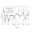
- FIG. 2 shows scaled versions of the transmit signal envelope and the power amplifier supply voltage along with a digital reference signal. Slight distortions mainly due to filtering imperfections and local oscillator (LO) leakage create mismatches between the signals which result in out-of-band noise at the power amplifier output.
- LO local oscillator
- FIG. 3 shows a partial block diagram of a chip (30) where the signal envelope is calculated in the digital domain in direct conversion receiver architecture.
- digital I and Q (in-phase and quadrature) samples (32,34) are fed to respective digital-to-analog converters (35, 37), each having a respective analog output fed to respective I/Q filters (39,41) and thence to variable gain I and Q amplifiers (43, 45).
- the amplified outputs are fed to respective mixers (47,49) where they are mixed with in-phase and quadrature versions of a local oscillator frequency (LO, LO').
- the mixer outputs are combined together and fed to a buffer/driver (51) and output to a power amplifier and antenna (not shown).
- the digital I and Q samples (32,34) are also fed to a processing path (33) which first (55) calculates I 2 (t) + Q 2 (t).
- the squaring doubles the frequency space occupied by the signal with respect to the transmit signal bandwidth. Therefore, the I/Q sampling frequency must be high enough to avoid aliasing.
- gain (57) and delay (59) are adjusted so that they match as closely as possible the delay and gain in the transmit path (and any gain and delay off-chip).
- a mapping or shaping function (61) is applied to relate the instantaneous signal amplitude to the required power amplifier voltage, before conversion to analog in an envelope digital-to-analog converter (63) and passing through an envelope filter (65).
- mapping function is specific to the power amplifier design but conventionally it may consist of a minimum constant level corresponding to a minimum voltage required by the power amplifier for small signals (typically around 1.0V) and a non-linear term closely following a square-root profile for larger signal amplitudes.
- the transition region between flat region and square-root profile is smoothed to avoid creating high harmonic content when the signal moves through the transition region.
- One possible implementation for the mapping function is a look-up table.
- FIG. 4 shows the spectra of a filtered 20MHz 100RB LTE uplink signal and its envelope on a 1 GHz carrier (for illustration).
- the envelope signal has significant power contributions (around -10 dBV/MHz) beyond twice the bandwidth of the transmit signal.
- the envelope filter (65) has a cut-off frequency well beyond the transmit signal bandwidth. This, however, means that any quantization noise from the envelope digital-to-analog converter (63) is not efficiently filtered and digital-to-analog converter noise thus will appear on the power amplifier voltage supply. This means that the envelope digital-to-analog converter (63) needs to be a very high precision digital-to-analog converter if FDD bands with small duplex spacing are to be supported.
- the envelope digital-to-analog converter (63) is not the only circuit with challenging requirements. Because mismatches between the envelope signal (Env) and the transmit signal (TX) have to be kept to a minimum, very stringent requirements have to be placed on all circuitry generating these signals.
- the timing mismatch between the transmit signal and envelope signal is ideally in the region of 1ns to maximize the power amplifier efficiency.
- This also means that the group delay ripple of both I/Q filters (39, 41) and envelope filter (65) are to be well below a few nanoseconds.
- the gain response would need to be very flat. More stringent requirements likely result in a higher power consumption and reduce the power saving benefit of the envelope tracking scheme.
- envelope distortion of different blocks in the signal chain add up as root of sum of squares of the individual envelope distortion contributions. This allows quantifying of the contributions from different circuit blocks.
- the envelope distortion contribution is the same as the contribution to EVM.
- LO leakage does not contribute to EVM in LTE systems as the subcarrier at zero offset carries no data. However, it does contribute to envelope distortion.
- envelope distortion metric For example, -25dBc LO leakage is equivalent to 5.6% envelope distortion or 2.8ns relative delay. For a realistic system the total envelope distortion combining all impairments will be in the order of 10% equivalent to 5ns delay.
- a power amplifier operating in a linear region (substantially constant gain versus input power) is fairly forgiving to imperfections.
- the same amplifier operated in non-linear conditions, for example in a compression region amplifies imperfections. For example, LO leakage is a phenomenon where an extra tone is added into the transmit signal. If the power amplifier is linear this tone is passed through. If, however, the power amplifier is run at 2dB compression the gain will move up and down with the extra tone present and this will create mixing products.
- a method of transmitting an RF signal derived from baseband samples comprising modulating information derived from the baseband samples onto a RF carrier, and amplifying the modulated signal in an amplifier, wherein the step of amplifying comprises applying a voltage mapping to the amplitude of the baseband samples to control the amplifier supply, wherein the voltage mapping is a linear function of the square of the amplitude of the baseband samples.
- the method may comprise converting a digital signal to analog to form said resultant signal.
- mapping function is typically constructed such that the power efficiency of the power amplifier is maximized whilst at the same time the linearity requirements are met. This particular choice of mapping function is referred to herein as the "power mapping function”.
- the method may further comprise determining a power mapping signal, and forming the voltage mapping to be tangential to the power mapping signal.
- the method may further comprise selecting a point on the power mapping signal at which the voltage mapping signal is tangential to the power mapping signal.
- the point is a point corresponding to the average of the baseband signal amplitude squared.
- the point is in a range between 0.75 times the square of the average signal amplitude and 3 times the square of the average signal amplitude.
- the point is selected based upon out-of-band noise requirements.
- the RF signal may be a signal meeting LTE standards.
- a transceiver having a transmitter configured to transmit, via a transmit antenna, an RF signal derived from baseband samples and a receiver for receiving signals from a receive antenna, the transmitter comprising a modulator for modulating information derived from the baseband samples onto a RF carrier, and an amplifier for amplifying the modulated signal for application to the transmit antenna, wherein the transmitter comprises processing circuitry for deriving a amplitude signal indicative of the instantaneous amplitude squared of the baseband samples, the processing circuitry configured to apply a voltage mapping to the amplitude signal to provide a resultant signal and an envelope modulator for using the resultant signal to control the voltage applied to the amplifier, wherein the voltage mapping is a linear function of the square of the amplitude of the baseband samples.
- the transceiver may be a frequency division duplex transceiver wherein the transmit and receive antennas are a single duplex antenna.
- the FDD transceiver may be adapted for LTE signals.
- the envelope signal is modified so that voltage headroom is provided to the power amplifier.
- This headroom may be scalable so that it can be adjusted depending on the power amplifier output noise requirements.
- power amplifier output noise is not critical (e.g. for TDD bands or FDD bands with large duplex spacing) or where power amplifier noise in the receive band is known to be lower (e.g. because of narrow transmit bandwidth or low transmit power) the headroom can be reduced so that the full power efficiency gain of the envelope tracking scheme can be exploited.
- the headroom can be increased in order to accommodate any circuit impairments.
- This disclosure proposes a different way of providing voltage headroom.
- ⁇ .. ⁇ signifies the time average over a suitably large duration.
- the power mapping function approximately follows a square-root profile at least for large signal amplitudes.
- the power mapping function can be approximated to be M + d t / 2 ⁇ M .
- This disclosure suggests a mapping function that is tangential to this power mapping function and is linear.
- M is the parameter that relates to this choice.
- Figure 5 shows the power mapping function (which, as noted above, maximizes power amplifier efficiency) compared to a linear approximation.
- the disclosure is of particular importance to LTE transceivers.
- the LTE signal is formed such that most of the time its amplitude is close to the average amplitude - see Figure 6a .
- the CCDF plot resolves very well the very low probability tail-end of the distribution where the signal power is well above the average. However, the PA will clip signals larger than around 4-5dB above the RMS power. The resultant out-of-band power is acceptable.
- the supply voltage associated with the very highest signal peaks will also be high.
- a practical power supply will not be able to exceed a certain supply level and will also start clipping the supply peaks.
- the supply would hit the limit more often than with the power mapping function because it's trying to achieve a greater headroom.
- the supply voltage with the linear mapping will be at least as high and typically higher than with the power mapping and therefore the average unwanted out-of-band products are lower.
- the parameter M can be selected according to needs. Close to one for aggressive power optimization when out-of-band noise is not an issue (e.g. when overall TX power is low or signal bandwidth is low) or higher up on the curve when the out-of-band noise must be controlled.
- Figure 7 shows spectra of a filtered 20MHz LTE uplink signal, its envelope and the linear approximation of the envelope signal at one a 1 GHz carrier (for illustration).
- the linear approximation means the power amplifier voltage signal is confined to twice the transmit signal bandwidth.
- the digital-to-analog converter sampling frequency may be as low as four times the signal rate and a filter in the envelope path can effectively remove any digital-to-analog converter noise at the duplex spacing frequency. This drastically reduces the digital-to-analog converter precision requirements.
- the lower signal bandwidth of the envelope signal path also means that the power supply for the envelope tracking does not need to follow frequencies beyond twice the signal bandwidth. This allows simplification of the design of the power supply and can allow its intrinsic efficiency to be increased.
- linear mapping Another advantage of the linear mapping is that the digital implementation is simplified. While the non-linear mapping is typically achieved using a look-up table which may involve large memory requirements, the linear mapping can be done efficiently using hard coded logic circuitry.
- the first order approximation is a strict upper bound to the square-root function. Therefore, the power amplifier power added efficiency is reduced.
- the exact level of reduction depends on the minimum voltage required by the power amplifier and also on the modulation scheme.
- the sacrificed power efficiency is surprisingly small. This is because the SC-FDMA modulation (used in LTE) achieves a signal whose amplitude distribution is closely concentrated around the average power level.
- the amount of average headroom is also adjustable through the parameter M as defined above.
- Figure 8 shows three plots of mapping function output with time for an LTE 100 RB uplink signal, as the lowest plot (solid line).
- the model is of a 20MHz 100RB LTE uplink signal, with analysis restricted to a single impairment, a relative delay between transmit signal and power amplifier voltage signal.
- the relative delay results in envelope distortion as defined above.
- the relation between the two is shown in Figure. 9 , which shows power amplifier output noise as a function of delay mismatch for the power mapping function (achieving 67.4% power added efficiency) and for applied constant headroom of 10%, 20% and 30% of the mean value of the power mapping voltage signal.
- the power density is measured outside the transmit band.
- the most critical out-of-band requirement may be at different frequency offsets. Focus here is on the noise density at 50MHz offset from the transmit carrier where the aim is for a noise density of -135dBm/Hz.
- Figure 12 shows the power amplifier power-added efficiency as a trade-off against the allowable signal mismatch.
- the target noise power density at 50MHz offset from the LTE uplink carrier is set to -135dBm/Hz.
- the curve marked "linear mapping function” shows the performance of the proposed scheme.
- the curve marked "power mapping function and constant headroom” provides a comparison for the technique where constant headroom is added.
- the "no envelope tracking" curve shows the power added efficiency of the power with constant supply voltage. All points achieve a noise level of -135dBm/Hz at 50MHz from the LTE carrier at full power.
- the disclosure envisages a scheme where the mapping function relating instantaneous signal amplitude squared to power amplifier voltage is linearized.
- the linearization adds headroom to the power amplifier voltage supply which means some power efficiency is sacrificed.
- the scheme of using an envelope signal with the linear relation to the square of the instantaneous signal amplitude reduces the envelope signal bandwidth and thereby allows significant relaxation of requirements on the circuit design, in particular digital-to-analog converter precision and filtering requirements but also requirements on the ET power supply.
- the linear approximation provides a flexible supply voltage headroom to the power amplifier which maybe tuned according to the transmission scenario (band, occupied signal bandwidth, transmit power level).
- the headroom makes the system more tolerant to impairments like delay mismatch between transmit signal and envelope signal. This leads to further easing of design constraints and can also reduce the amount of production calibration necessary.
- I and Q signals are associated with certain types of transmitter architectures (quadrature modulators). However, in any system there will be a baseband representation of the RF signal that is ultimately transmitted. All that is then necessary in the digital processing domain is to calculate the square of the signal amplitude. Depending on how the signal is represented this can be performed in different ways but it will always be possible. If the signal is presented as real and imaginary part then the preceding explanation applies. If the signal is represented in polar coordinates, for example, then the amplitude is already known and only needs to be squared.
Landscapes
- Engineering & Computer Science (AREA)
- Power Engineering (AREA)
- Amplifiers (AREA)
- Transmitters (AREA)
Priority Applications (2)
| Application Number | Priority Date | Filing Date | Title |
|---|---|---|---|
| EP12170564.4A EP2670047A1 (fr) | 2012-06-01 | 2012-06-01 | Communications RF |
| US13/907,092 US9496838B2 (en) | 2012-06-01 | 2013-05-31 | Envelope tracking amplifier for a transmitter having a voltage mapping linearly related to the square of the amplitude of the baseband signal |
Applications Claiming Priority (1)
| Application Number | Priority Date | Filing Date | Title |
|---|---|---|---|
| EP12170564.4A EP2670047A1 (fr) | 2012-06-01 | 2012-06-01 | Communications RF |
Publications (1)
| Publication Number | Publication Date |
|---|---|
| EP2670047A1 true EP2670047A1 (fr) | 2013-12-04 |
Family
ID=46466102
Family Applications (1)
| Application Number | Title | Priority Date | Filing Date |
|---|---|---|---|
| EP12170564.4A Withdrawn EP2670047A1 (fr) | 2012-06-01 | 2012-06-01 | Communications RF |
Country Status (2)
| Country | Link |
|---|---|
| US (1) | US9496838B2 (fr) |
| EP (1) | EP2670047A1 (fr) |
Families Citing this family (4)
| Publication number | Priority date | Publication date | Assignee | Title |
|---|---|---|---|---|
| US9391649B2 (en) | 2014-11-17 | 2016-07-12 | Microsoft Technology Licensing, Llc | Envelope shaping in envelope tracking power amplification |
| US9813029B2 (en) * | 2015-06-30 | 2017-11-07 | Skyworks Solutions, Inc. | Differential amplifier linearization in a radio frequency system |
| JP6665565B2 (ja) * | 2016-02-08 | 2020-03-13 | 株式会社富士通ゼネラル | 電力増幅装置 |
| CN115473541A (zh) * | 2021-05-24 | 2022-12-13 | 深圳市万普拉斯科技有限公司 | 射频调节方法及射频电路、电子设备、可读存储介质 |
Citations (3)
| Publication number | Priority date | Publication date | Assignee | Title |
|---|---|---|---|---|
| GB2345212A (en) * | 1997-12-31 | 2000-06-28 | Motorola Inc | An arrangement for controlling the supply of an rf power amplifier in dependence on the envelope of the baseband input |
| WO2004001958A1 (fr) * | 2002-06-19 | 2003-12-31 | Telefonaktiebolaget Lm Ericsson (Publ) | Production efficace de courants haute frequence |
| WO2004019486A1 (fr) * | 2002-08-21 | 2004-03-04 | Siemens Aktiengesellschaft | Systeme amplificateur de puissance |
Family Cites Families (4)
| Publication number | Priority date | Publication date | Assignee | Title |
|---|---|---|---|---|
| US20110150038A1 (en) * | 2009-10-27 | 2011-06-23 | Victor Korol | System and method for uwb transmission predistortion and rf wire-bond interface technique related application |
| US8854128B2 (en) * | 2010-01-14 | 2014-10-07 | Sumitomo Electric Industries, Ltd. | Amplifying device and signal processing device |
| US8447245B2 (en) * | 2010-01-22 | 2013-05-21 | Freescale Semiconductor, Inc. | Radio frequency transmitter having an amplifier with power supply modulation |
| US8718188B2 (en) * | 2011-04-25 | 2014-05-06 | Skyworks Solutions, Inc. | Apparatus and methods for envelope tracking |
-
2012
- 2012-06-01 EP EP12170564.4A patent/EP2670047A1/fr not_active Withdrawn
-
2013
- 2013-05-31 US US13/907,092 patent/US9496838B2/en active Active
Patent Citations (3)
| Publication number | Priority date | Publication date | Assignee | Title |
|---|---|---|---|---|
| GB2345212A (en) * | 1997-12-31 | 2000-06-28 | Motorola Inc | An arrangement for controlling the supply of an rf power amplifier in dependence on the envelope of the baseband input |
| WO2004001958A1 (fr) * | 2002-06-19 | 2003-12-31 | Telefonaktiebolaget Lm Ericsson (Publ) | Production efficace de courants haute frequence |
| WO2004019486A1 (fr) * | 2002-08-21 | 2004-03-04 | Siemens Aktiengesellschaft | Systeme amplificateur de puissance |
Also Published As
| Publication number | Publication date |
|---|---|
| US20140018133A1 (en) | 2014-01-16 |
| US9496838B2 (en) | 2016-11-15 |
Similar Documents
| Publication | Publication Date | Title |
|---|---|---|
| KR101821294B1 (ko) | 감소된 대역폭 이티 및 디피디 처리장치 및 그 처리방법 | |
| US8095093B2 (en) | Multi-mode transmitter having adaptive operating mode control | |
| EP3032738B1 (fr) | Procédé et appareil pour corriger des caractéristiques de charge d'un amplificateur de puissance incorrectes dans un système à base de repérage d'enveloppe | |
| US8879665B2 (en) | Controlling a power amplifier based on transmitter output emissions | |
| US8081935B2 (en) | Multiple-mode modulator to process baseband signals | |
| EP3061184B1 (fr) | Largeur de bande réduite de signal dans un chemin d'enveloppe d'un système de suivi d'enveloppe | |
| CN100589462C (zh) | 宽带码分多址基站系统多通道多载波数字预失真发信机 | |
| EP2169837B1 (fr) | Technique pour supprimer le bruit dans un dispositif de transmetteur | |
| US20140355718A1 (en) | Device for modifying trajectories | |
| JP6119735B2 (ja) | 送信装置および送信方法 | |
| US8489046B2 (en) | Signal decomposition methods and apparatus for multi-mode transmitters | |
| JP6827613B2 (ja) | 衛星信号伝送システムにおける予歪み | |
| US20140135050A1 (en) | Method and apparatus for improving efficiency and distortion leakage in awireless power amplifier | |
| US20140233677A1 (en) | Method and equipment for controlling radio-frequency signal | |
| US9496838B2 (en) | Envelope tracking amplifier for a transmitter having a voltage mapping linearly related to the square of the amplitude of the baseband signal | |
| US9668208B2 (en) | Operating point setting of an amplifier | |
| US8131233B2 (en) | Time alignment methods and apparatus for polar modulation transmitters | |
| Talonen et al. | System requirements for OFDM polar transmitter | |
| US9853608B2 (en) | Temperature compensation technique for envelope tracking system | |
| WO2005076495A1 (fr) | Procedes d'amelioration de la linearite d'un amplificateur de puissance | |
| EP2568754A1 (fr) | Étalonnage d'émetteur dynamique | |
| Yang et al. | A polar transmitter using interleaving pulse modulation for multimode handsets | |
| CN106664179A (zh) | 载波聚合信号的波峰因子降低 | |
| CN117559918A (zh) | 一种电压校正方法、设备和存储介质 | |
| JP2009033250A (ja) | 送信装置 |
Legal Events
| Date | Code | Title | Description |
|---|---|---|---|
| PUAI | Public reference made under article 153(3) epc to a published international application that has entered the european phase |
Free format text: ORIGINAL CODE: 0009012 |
|
| AK | Designated contracting states |
Kind code of ref document: A1 Designated state(s): AL AT BE BG CH CY CZ DE DK EE ES FI FR GB GR HR HU IE IS IT LI LT LU LV MC MK MT NL NO PL PT RO RS SE SI SK SM TR |
|
| AX | Request for extension of the european patent |
Extension state: BA ME |
|
| 17P | Request for examination filed |
Effective date: 20140529 |
|
| RBV | Designated contracting states (corrected) |
Designated state(s): AL AT BE BG CH CY CZ DE DK EE ES FI FR GB GR HR HU IE IS IT LI LT LU LV MC MK MT NL NO PL PT RO RS SE SI SK SM TR |
|
| STAA | Information on the status of an ep patent application or granted ep patent |
Free format text: STATUS: THE APPLICATION IS DEEMED TO BE WITHDRAWN |
|
| 18D | Application deemed to be withdrawn |
Effective date: 20190103 |