EP2671294B1 - Vorrichtung mit einem laser - Google Patents
Vorrichtung mit einem laser Download PDFInfo
- Publication number
- EP2671294B1 EP2671294B1 EP12702454.5A EP12702454A EP2671294B1 EP 2671294 B1 EP2671294 B1 EP 2671294B1 EP 12702454 A EP12702454 A EP 12702454A EP 2671294 B1 EP2671294 B1 EP 2671294B1
- Authority
- EP
- European Patent Office
- Prior art keywords
- laser
- stripe
- lateral
- corrugations
- output
- Prior art date
- Legal status (The legal status is an assumption and is not a legal conclusion. Google has not performed a legal analysis and makes no representation as to the accuracy of the status listed.)
- Active
Links
Images





Classifications
-
- H—ELECTRICITY
- H01—ELECTRIC ELEMENTS
- H01S—DEVICES USING THE PROCESS OF LIGHT AMPLIFICATION BY STIMULATED EMISSION OF RADIATION [LASER] TO AMPLIFY OR GENERATE LIGHT; DEVICES USING STIMULATED EMISSION OF ELECTROMAGNETIC RADIATION IN WAVE RANGES OTHER THAN OPTICAL
- H01S5/00—Semiconductor lasers
- H01S5/10—Construction or shape of the optical resonator, e.g. extended or external cavity, coupled cavities, bent-guide, varying width, thickness or composition of the active region
- H01S5/1003—Waveguide having a modified shape along the axis, e.g. branched, curved, tapered, voids
-
- H—ELECTRICITY
- H01—ELECTRIC ELEMENTS
- H01S—DEVICES USING THE PROCESS OF LIGHT AMPLIFICATION BY STIMULATED EMISSION OF RADIATION [LASER] TO AMPLIFY OR GENERATE LIGHT; DEVICES USING STIMULATED EMISSION OF ELECTROMAGNETIC RADIATION IN WAVE RANGES OTHER THAN OPTICAL
- H01S5/00—Semiconductor lasers
- H01S5/40—Arrangement of two or more semiconductor lasers, not provided for in groups H01S5/02 - H01S5/30
- H01S5/4025—Array arrangements, e.g. constituted by discrete laser diodes or laser bar
- H01S5/4031—Edge-emitting structures
- H01S5/4068—Edge-emitting structures with lateral coupling by axially offset or by merging waveguides, e.g. Y-couplers
-
- H—ELECTRICITY
- H01—ELECTRIC ELEMENTS
- H01S—DEVICES USING THE PROCESS OF LIGHT AMPLIFICATION BY STIMULATED EMISSION OF RADIATION [LASER] TO AMPLIFY OR GENERATE LIGHT; DEVICES USING STIMULATED EMISSION OF ELECTROMAGNETIC RADIATION IN WAVE RANGES OTHER THAN OPTICAL
- H01S2301/00—Functional characteristics
- H01S2301/16—Semiconductor lasers with special structural design to influence the modes, e.g. specific multimode
- H01S2301/166—Single transverse or lateral mode
-
- H—ELECTRICITY
- H01—ELECTRIC ELEMENTS
- H01S—DEVICES USING THE PROCESS OF LIGHT AMPLIFICATION BY STIMULATED EMISSION OF RADIATION [LASER] TO AMPLIFY OR GENERATE LIGHT; DEVICES USING STIMULATED EMISSION OF ELECTROMAGNETIC RADIATION IN WAVE RANGES OTHER THAN OPTICAL
- H01S2301/00—Functional characteristics
- H01S2301/18—Semiconductor lasers with special structural design for influencing the near- or far-field
-
- H—ELECTRICITY
- H01—ELECTRIC ELEMENTS
- H01S—DEVICES USING THE PROCESS OF LIGHT AMPLIFICATION BY STIMULATED EMISSION OF RADIATION [LASER] TO AMPLIFY OR GENERATE LIGHT; DEVICES USING STIMULATED EMISSION OF ELECTROMAGNETIC RADIATION IN WAVE RANGES OTHER THAN OPTICAL
- H01S5/00—Semiconductor lasers
- H01S5/10—Construction or shape of the optical resonator, e.g. extended or external cavity, coupled cavities, bent-guide, varying width, thickness or composition of the active region
- H01S5/1003—Waveguide having a modified shape along the axis, e.g. branched, curved, tapered, voids
- H01S5/101—Curved waveguide
-
- H—ELECTRICITY
- H01—ELECTRIC ELEMENTS
- H01S—DEVICES USING THE PROCESS OF LIGHT AMPLIFICATION BY STIMULATED EMISSION OF RADIATION [LASER] TO AMPLIFY OR GENERATE LIGHT; DEVICES USING STIMULATED EMISSION OF ELECTROMAGNETIC RADIATION IN WAVE RANGES OTHER THAN OPTICAL
- H01S5/00—Semiconductor lasers
- H01S5/10—Construction or shape of the optical resonator, e.g. extended or external cavity, coupled cavities, bent-guide, varying width, thickness or composition of the active region
- H01S5/1053—Comprising an active region having a varying composition or cross-section in a specific direction
- H01S5/1064—Comprising an active region having a varying composition or cross-section in a specific direction varying width along the optical axis
-
- H—ELECTRICITY
- H01—ELECTRIC ELEMENTS
- H01S—DEVICES USING THE PROCESS OF LIGHT AMPLIFICATION BY STIMULATED EMISSION OF RADIATION [LASER] TO AMPLIFY OR GENERATE LIGHT; DEVICES USING STIMULATED EMISSION OF ELECTROMAGNETIC RADIATION IN WAVE RANGES OTHER THAN OPTICAL
- H01S5/00—Semiconductor lasers
- H01S5/10—Construction or shape of the optical resonator, e.g. extended or external cavity, coupled cavities, bent-guide, varying width, thickness or composition of the active region
- H01S5/11—Comprising a photonic bandgap structure
-
- H—ELECTRICITY
- H01—ELECTRIC ELEMENTS
- H01S—DEVICES USING THE PROCESS OF LIGHT AMPLIFICATION BY STIMULATED EMISSION OF RADIATION [LASER] TO AMPLIFY OR GENERATE LIGHT; DEVICES USING STIMULATED EMISSION OF ELECTROMAGNETIC RADIATION IN WAVE RANGES OTHER THAN OPTICAL
- H01S5/00—Semiconductor lasers
- H01S5/10—Construction or shape of the optical resonator, e.g. extended or external cavity, coupled cavities, bent-guide, varying width, thickness or composition of the active region
- H01S5/12—Construction or shape of the optical resonator, e.g. extended or external cavity, coupled cavities, bent-guide, varying width, thickness or composition of the active region the resonator having a periodic structure, e.g. in distributed feedback [DFB] lasers
- H01S5/1237—Lateral grating, i.e. grating only adjacent ridge or mesa
-
- H—ELECTRICITY
- H01—ELECTRIC ELEMENTS
- H01S—DEVICES USING THE PROCESS OF LIGHT AMPLIFICATION BY STIMULATED EMISSION OF RADIATION [LASER] TO AMPLIFY OR GENERATE LIGHT; DEVICES USING STIMULATED EMISSION OF ELECTROMAGNETIC RADIATION IN WAVE RANGES OTHER THAN OPTICAL
- H01S5/00—Semiconductor lasers
- H01S5/20—Structure or shape of the semiconductor body to guide the optical wave ; Confining structures perpendicular to the optical axis, e.g. index or gain guiding, stripe geometry, broad area lasers, gain tailoring, transverse or lateral reflectors, special cladding structures, MQW barrier reflection layers
- H01S5/2036—Broad area lasers
Definitions
- the present invention relates to a semiconductor lasers, and more particularly to high-brightness edge-emitting semiconductor laser diodes or diode arrays.
- the invention refers to diodes or diode arrays which emit high power with narrow divergence of the laser beam in the lateral direction.
- High-brightness edge-emitting semiconductor lasers are lasers that are characterized by high power and high beam quality of the output radiation. These semiconductor optical sources are attractive for use in a variety of applications including, for example, industrial material processing, pumping of fiber amplifiers, fiber and solid state lasers, free space communications, second harmonic generation, medicine, laser printing, lidar.
- the emission of high-brightness lasers shows conveniently an approximately constant spot size over significant propagation distances (far-field zone) and is suitable for a variety of direct applications, without using external focusing optical systems of large complexity.
- High-brightness lasers are supposed to radiate high power and simultaneously have small spatial angle (small divergence) of the radiation in both vertical direction (direction of the epitaxial growth) and lateral direction (parallel to the epitaxial plane).
- the brightness of a laser source is generally understood as the power divided by the mode area in the focus and the spatial solid angle in the far-field.
- the brightness is reduced by the product of the M2 factors of the beam quality for the vertical and lateral direction.
- the M2 factor is defined as the product of beam radius at the beam waist and the far-field beam divergence angle divided by the corresponding product for a diffraction-limited Gaussian beam with the same wavelength.
- Typical high-power edge-emitting lasers have a large divergence in the vertical direction and a low beam quality in the lateral direction. They consist typically of a vertical sub-pm-sized single-mode epitaxial layer waveguide of III-IV or II-VI semiconductor materials and a multi-mode laterally etched waveguide of a width of several tens of ⁇ m. This results in the M2 beam quality factor in the lateral direction which is typically much higher than in the vertical direction due to the emission of a multitude of higher order modes. Such a radiation cannot be focused to a small spot, needed for most applications, even using complicated external focusing optical systems.
- a number of different approaches are known to obtain high-power semiconductor lasers with small divergence in the vertical direction.
- a concept of large optical cavity with low index-contrast GaAs/AlGaAs waveguide in the vertical direction was developed which resulted in ⁇ 1 W single-mode power and a vertical beam divergence of -10° (see Ref. [1] and references therein).
- Another concept of high-brightness semiconductor lasers employs a thick vertical waveguide formed by a quasi-periodic multi-layered GaAs/AlGaAs sequence known as a vertical photonic bandgap crystal (PBC lasers) [2].
- PBC lasers vertical photonic bandgap crystal
- This approach has allowed generating a narrow vertical beam divergence down to 5° or less at different wavelength ranges from the visible to the near-infrared.
- the PBC laser approach is applicable also to other laser diode material systems e.g. based on (Al,Ga,In)N/GaN semiconductor materials, generating light in the UV-green range.
- An alternative concept is based on a leaky-wave laser design providing output of the laser emission through a thick transparent substrate with extremely narrow beam divergence of ⁇ 1° [3-4].
- the output power of edge-emitting semiconductor lasers and output beam quality in the lateral direction are defined by the lateral laser structure which provides the optical field confinement in this direction and simultaneously supplies the pump current to the active area.
- the lateral laser structure is comprised of an etched stripe characterized by different refractive indices in the stripe cross-section and coinciding with the current contact. With increasing stripe area, the pump current and hence the emitted laser power increase, as the power is approximately proportional to the current. The latter relation is valid up to the onset of thermally induced current-spreading and gain hole-burning nonlinear effects.
- Narrow single stripes provide a single-mode radiation with single-lobed far-field in the lateral direction but yield no high power, since no high enough currents are possible. Widening of the stripe allows to launch high current and increase the output power, however inevitably worsens the output beam quality due to lasing of higher-order lateral modes of a wide waveguide stripe characterized by multi-lobe far fields.
- a tapered stripe geometry presents an effective design to combine the desirable operational characteristics of high power and narrow output beam with simple, low cost device fabrication (see Ref. [5] and references therein).
- the fundamental lateral mode corresponding to the narrow end of the taper have diffraction-free propagation and amplification along the whole extent of the stripe, including the wide end of the stripe.
- Higher-order lateral modes of the wide taper part are discriminated at the narrow end and make up only a small portion of the laser emission at the output facet.
- the output emission of the tapered laser consists mostly of the fundamental lateral mode which corresponds to the wide taper part near the output facet, showing a single-lobe far field.
- the output power can be rather large due to the large total contact area. Both these factors made tapered lasers to be a promising approach for development of high-brightness diode lasers.
- a modification of the tapered stripe lasers is also known, where the wide stripe of the diode laser has a narrow part in the middle leading to the shape of a "bow-tie" waveguide [6].
- supermodes have different phase relations between the electromagnetic fields emitted from each of the stripes considered as individual light sources. Only the mode with equal phase from all stripes (in-phase mode) or the mode with pi-shifted phases (out-of-phase mode) along the whole array cross-section are of interest for achieving a high brightness.
- the in-phase and out-of-phase supermodes have single- or double-lobe far fields, respectively, and are suitable for applications.
- a presence of other supermodes with different phase shifts deteriorates the output beam quality, since they show a multi-lobe far field.
- the challenge remains to achieve a high lateral beam quality, since the multiple supermodes of the arrays equally contribute to the output, because they are degenerated by confinement factors and losses.
- the discrimination of multiple lateral modes in favor of the desired single mode remains weak and/or too sensitive to the variations of the laser operational conditions (as in the case of diffraction coupling and Talbot filter). Differences obtained in the confinement factors and losses of the in-phase or out-of-phase mode (as well as any preferable single lateral mode) as compared to other lateral modes are too small.
- a device comprising the features according to the preamble of claim 1 is disclosed in US Patent Application Publication US2006/0193353 A1 .
- a laser diode with corrugations is disclosed in US 5,084,892 .
- An objective of the present invention is to provide a device, which provides radiation with small divergence in lateral direction in the fundamental mode.
- An embodiment of the invention relates to a device comprising the features of claim 1.
- the waveguide stripe comprises triangular-shape corrugations provided with saw-tooth orientation with respect to the laser output facet and with the orientation of the wider triangular side towards the laser's output facet or towards the laser's rear facet, wherein the triangular-shape corrugations are symmetric with respect to the longitudinal axis.
- the corrugations are configured to provide additional radiation losses of higher-order lateral modes compared to the fundamental lateral mode by scattering radiation into the lateral directions. The losses provide that the output radiation is single-mode and that the far field has a single-lobe with small divergence.
- the laser is an edge-emitting semiconductor laser diode.
- the waveguide stripe may be coupled to or may be part of the active region of the edge-emitting semiconductor laser diode.
- the waveguide stripe may comprise triangular-shape corrugations with the orientation of the wider triangular side towards the laser's output facet. Additionally, or alternatively, the wider triangular side may be oriented towards the laser's rear facet.
- the waveguide stripe may also comprise rectangular-shape corrugations which are inclined towards the output facet direction and symmetrical with respect to the longitudinal axis.
- the rectangular-shape corrugations may be inclined towards the output facet direction and asymmetrical with respect to the longitudinal axis.
- the diode laser preferably comprises at least one heterostructure consisting of III-IV or II-VI semiconductor material, e. g. AlGaAs/GaAs, InGaAs/GaAs, InGaAsP/GaAs, ZnMgSSe/ZnSSe, (Al,Ga,In)N/GaN, said heterostructure forming a quantum well, quantum dot or quantum cascade laser.
- III-IV or II-VI semiconductor material e. g. AlGaAs/GaAs, InGaAs/GaAs, InGaAsP/GaAs, ZnMgSSe/ZnSSe, (Al,Ga,In)N/GaN, said heterostructure forming a quantum well, quantum dot or quantum cascade laser.
- a further embodiment of the invention relates to a method of fabricating a device according to claim 8.
- embodiments of the present invention provide high lateral beam quality for high-brightness edge-emitting semiconductor lasers. This is preferably achieved by employing a longitudinal inhomogeneity of the stripes and/or a lateral coupling of the stripes, which provides high losses for higher-order lateral modes and preferable guiding of in-phase supermodes, respectively.
- This mode discrimination are obtained by means of a corrugated shape of the stripe.
- Standard processing technology allows forming the corrugated boundaries of the stripes with characteristic sizes of the corrugations of the order of several wavelengths which are sufficient to provide a substantial discrimination.
- the method is applicable to different quantum well, quantum dot and quantum cascade semiconductor lasers generating in the ranges from the ultraviolet to the far-infrared.
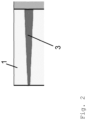
- Figure 1 shows a top view of a typical prior art single-stripe semiconductor laser 1.
- the lateral and longitudinal directions are designated by reference numerals x and z, respectively.
- the laser 1 inter alia comprises a wave guiding stripe 3, a rear facet 4, and an output facet 5.
- the free space outside the laser is designated by reference numeral 6.
- the refractive index of the stripe 3 is larger than the refractive index of the outer areas 7 in order to provide wave guiding in the lateral direction.
- the output and the rear facets have high reflective and low reflective coatings, respectively, consisting of several layers (not shown) of low refractive index materials with definite thicknesses.
- embodiments of the present invention are based on the suppression of higher-order lateral modes in favor of the fundamental mode in order to provide a single-lobe far field.
- the devices according to Figures 3-10 comprise longitudinally corrugated stripes 3'.
- the width of the stripes 3' is wide enough to allow multimode propagation of radiation along the longitudinal direction.
- the corrugations of the waveguide stripes 3' in the longitudinal direction cause large losses for higher-order lateral modes by increased scattering as compared to the fundamental lateral mode.
- the output radiation is single-mode (despite the large stripe width which would allow multimode propagation), and results in a single-lobe far field with narrow divergence in the lateral direction, which means high brightness.
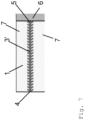
- FIG. 3 shows a first exemplary embodiment of a device comprising a single-stripe semiconductor laser 1 in further detail.
- the laser 1 may be formed by a multi-layered heterostructure consisting of III-IV or II-VI semiconductor materials, e. g. AlGaAs/GaAs, InGaAs/GaAs, InGaAsP/GaAs, ZnMgSSe/ZnSSe, (Al,Ga,In)N/GaN.
- the structure including the layers with e.g. quantum wells provide wave guiding in the vertical direction and gain.
- the laser 1 according to Figure 3 comprises a longitudinally inhomogeneous waveguide stripe 3'. At both edges of the waveguide stripe 3', triangular-shape corrugations are provided with "saw-tooth" orientation with respect to the laser output facet 5.
- the refractive index of the stripe 3' is larger than the refractive index of the outer areas 7 in order to provide wave guiding in the lateral direction.
- both, wave guiding in the vertical and the lateral directions, as well as light amplification and laser output are performed in a well understood manner.
- the laser output occurs as a combination of the modes guided by the heterostructure with contributions from each mode defined by the mode confinement factor and loss.
- the triangular-shape corrugations may be provided at both edges along the entire length of the waveguide stripe 3', as shown Figure 3 .
- only one edge may be provided with corrugations and/or only waveguide sections of the waveguide stripe 3' (i.e. not the entire stripe) may have corrugations.
- Figure 4 shows a second exemplary embodiment of a device comprising a single-stripe semiconductor laser 1 in further detail.
- the laser 1 comprises a longitudinally inhomogeneous waveguide stripe 3' having triangular-shape corrugations with "saw-tooth" orientation with respect to the laser output facet 5.
- the "saw-tooth" orientation in Figure 4 is opposite to the orientation shown in Figure 3 .
- FIG. 5 shows a third exemplary embodiment, which is not part of the present invention as claimed, of a device comprising a single-stripe semiconductor laser 1 in further detail.
- the laser 1 comprises a longitudinally inhomogeneous waveguide stripe 3' having rectangular-shape corrugations which are symmetric with respect to the lateral axis.
- FIG. 6 shows a fourth exemplary embodiment, which is not part of the present invention as claimed, of a device comprising a single-stripe semiconductor laser 1 in further detail.
- the laser 1 comprises a longitudinally inhomogeneous waveguide stripe 3' having rectangular-shape corrugations which are asymmetric with respect to the lateral axis.
- FIG. 7 shows a fifth exemplary embodiment, which is not part of the present invention as claimed, of a device comprising a single-stripe semiconductor laser 1 in further detail.
- the laser 1 comprises a longitudinally inhomogeneous waveguide stripe 3' having inclined corrugations which are symmetric. At both sides of the lateral axis the corrugations are bent to the output facet direction with respect to the lateral axis.
- FIG 8 shows a sixth exemplary embodiment, which is not part of the present invention as claimed, of a device comprising a single-stripe semiconductor laser 1 in further detail.
- the laser 1 comprises a longitudinally inhomogeneous waveguide stripe 3' having inclined corrugations which are asymmetric. At both sides of the lateral axis, the corrugations are bent to opposite directions with respect to the lateral axis.
- Figure 9 shows a seventh exemplary embodiment, which is not part of the present invention as claimed, of a device comprising a single-stripe semiconductor laser 1 in further detail.
- the laser 1 comprises a longitudinally inhomogeneous waveguide stripe 3' having triangular-shape corrugations which are symmetric in respect to the lateral axis.
- FIG 10 shows an eighth exemplary embodiment, which is not part of the present invention as claimed, of a device comprising a single-stripe semiconductor laser 1 in further detail.
- the laser 1 comprises a longitudinally inhomogeneous waveguide stripe 3' having triangular-shape corrugations which are asymmetric in respect to the lateral axis.
- Boundary conditions corresponding to non-reflecting boundaries at the top, bottom and right side (perfectly matched layers) and perfectly conducting boundary at the left side of the computation domain can be used.
- the complex eigenvalue k obtained defines the frequency and the loss (lifetime) of the modes E(x,z) which take into account field diffraction and radiation into the lateral direction for the refractive index profile including the contribution of the stripe corrugation.
- the rear and output facets typically consisting of several layers with definite thicknesses and refractive indices, providing high reflection and anti-reflection, respectively, can also be taken into account in the refractive index profile n(x,z) for the solution of Eq. (1).
- Figures 11-13 show further embodiments, which are not part of the present invention as claimed, of devices having edge-emitting semiconductor lasers.
- the embodiments provide high power and low divergence in the lateral direction based on multi-stripe arrays with field-coupled multiple stripes.
- Far-order field coupling of the stripes provided by the waveguide structure, where each stripe couples with all the stripes in the same extent (not dominantly with the nearest neighbors) causes preferential guiding and amplification of the in-phase lateral supermode of the stripe array.
- the out-of-phase supermode of the stripe array has larger loss due to scattering at the stripe structure and contributes less to the output of the laser array. Radiation from multiple stripes is coherent and phase-locked, resulting in a single-lobe far field with small divergence in the lateral direction proportional to the number of the stripes.
- the exemplary embodiment shown in Figure 11 refers to a multiple-stripe semiconductor laser 1 with a netlike stripe structure 10.
- the netlike stripe structure 10 is a hexagonal structure for field coupling of two arrays 11 each of which consists of three straight stripes 12.
- the number of the straight stripes 12 in the vicinity of the rear and output laser facet is not limited by three as shown and could be arbitrary.
- the hexagonal openings 13 of the netlike stripe structure 10 have a lower refractive index than the wave guiding stripes 14 of the netlike stripe structure 10.
- the exemplary embodiment shown in Figure 12 also comprises a hexagonal structure 10, but no arrays of straight stripes.
- the hexagonal structure 10 consists of, but is not limited to, three periods in the lateral direction as shown and could be arbitrary.
- the low-index openings 13 of the stripe structure 10 have a hexagonal shape.
- the exemplary embodiment shown in Figure 13 comprises a netlike stripe structure 20 with round openings 13.
- the embodiment may or may not comprise straight stripes 12 as shown in Figure 11 .
- the netlike structure 20 consists of, but is not limited to, three periods in the lateral direction as shown and could be arbitrary.
- the round openings 13 have a lower refractive index than the waveguide stripes 14 of the netlike stripe structure 20.
- the embodiments shown in Figures 3-13 may consist of or comprise epitaxial layers of III-IV or II-VI semiconductor materials grown by metal organic vapor phase epitaxy (MOVPE) or molecular beam epitaxy (MBE).
- MOVPE metal organic vapor phase epitaxy
- MBE molecular beam epitaxy
- the single- or multi-stripe edge-emitting lasers may be manufactured by photolithography and ion-beam-assisted etching. This standard technology allows forming corrugated boundaries of the stripes with characteristic sizes of the corrugations of the order of several wavelengths which are sufficient to provide substantial discrimination of the higher-order lateral modes.
- the netlike stripe structures 10, and 20 as shown in Figures 11-13 may also be manufactured by photolithography and ion-beam-assisted etching.
- embodiments of the invention relate to single-stripe edge-emitting semiconductor lasers with a stripe with corrugated boundary between areas with different refractive indices across the stripe to achieve lower lateral divergence of the output emission.
- the corrugations cause the discrimination of the lateral modes in wide stripes due to higher losses of the higher-order modes scattered into the lateral directions as compared to the fundamental lateral mode.
- the output emission of the stripe has high power and low divergence of the far field both due to wider stripe width as compared to a straight stripe.
- a high-brightness diode laser may be made of a multiple-stripe array with coupling of the stripes through a stripe structure having a hexagonal, a round or another shape.
- Multiple-stripe arrays provide far-order field coupling of all stripes, where in-phase lateral supermode of the stripe array have smaller losses in the lateral direction than out-of-phase supermode, as well as all other lateral modes of the stripe array.
- the far field has a single-lobe pattern corresponding to an in-phase mode with the divergence defined by the total output aperture of the array.
- the radiation from multiple stripes is coherent and phase-locked, resulting in a single-lobe far field with narrow divergence in the lateral direction, being inversely proportional to the number of the stripes.
Landscapes
- Physics & Mathematics (AREA)
- Condensed Matter Physics & Semiconductors (AREA)
- General Physics & Mathematics (AREA)
- Electromagnetism (AREA)
- Optics & Photonics (AREA)
- Semiconductor Lasers (AREA)
- Lasers (AREA)
Claims (6)
- Vorrichtung, die eine kantenemittierende Halbleiter-Laserdiode und einen Wellenleiterstreifen umfasst, wobei dessen Breite eine Multimode-Fortpflanzung von Strahlung entlang der Längsachse des Wellenleiterstreifens erlaubt, wobei der Wellenleiterstreifen mindestens eine gewellte Kantensektion entlang dessen Längsachse aufweist,wobei die Wellungen ausgelegt sind zum Liefern zusätzlicher Strahlungsverluste der Lateralmoden höherer Ordnung im Vergleich zu der Grund-Lateralmode durch Streuung von Strahlung in den lateralen Richtungen, wobei die Verluste bewirken, dass die Ausgangsstrahlung single-mode ist und dass das Fernfeld eine einzige Keule mit kleiner Divergenz aufweist,dadurch gekennzeichnet, dass- der Wellenleiterstreifen zwischen einer hochreflektierenden Rückfacette und einer niederreflektierenden Ausgangsfacette der kantenemittierenden Halbleiter-Laserdiode angeordnet ist, und- der Wellenleiterstreifen dreieckförmige Wellungen umfasst, die mit Sägezahnorientierung in Bezug auf die Laserausgangsfacette (5) und mit der Orientierung der breiteren dreieckigen Seite zur Ausgangsfacette des Lasers oder zur Rückfacette des Lasers hin versehen sind, wobei die dreieckförmigen Wellungen in Bezug auf die Längsachse symmetrisch sind.
- Vorrichtung nach Anspruch 1, wobei die an beiden Kanten des Wellenleiterstreifens dreieckförmigen Wellungen mit Sägezahnorientierung in Bezug auf die Ausgangsfacette des Lasers versehen sind.
- Vorrichtung nach Anspruch 1, wobei die an beiden Kanten des Wellenleiterstreifens dreieckförmigen Wellungen mit Sägezahnorientierung in Bezug auf die Rückfacette des Lasers versehen sind.
- Vorrichtung nach Anspruch 1, wobei der Laser eine kantenemittierende Halbleiter-Laserdiode ist und der Wellenleiterstreifen mit der aktiven Region der kantenemittierenden Halbleiter-Laserdiode gekoppelt oder ein Teil von dieser ist.
- Vorrichtung nach Anspruch 1, wobei die Laserdiode mindestens eine Heterostruktur umfasst, die aus III-IV- oder II-VI-Halbleitermaterial besteht, z. B. AlGaAs/GaAs, InGaAs/GaAs, InGaAsP/GaAs, ZnMgSSe/ZnSSe, (Al,Ga,In)N/GaN, wobei die Heterostruktur einen Quantentopf-, Quantenpunkt- oder Quantenkaskadenlaser bildet.
- Verfahren zum Herstellen einer Vorrichtung, die eine kantenemittierende Halbleiter-Laserdiode umfasst, wobei ein Wellenleiterstreifen, der mindestens eine gewellte Kantensektion entlang dessen Längsachse aufweist, zwischen einer hochreflektierenden Rückfacette und einer niederreflektierenden Ausgangsfacette der kantenemittierenden Halbleiter-Laserdiode unter Verwendung eines oder mehrerer Schritte von Photolithographie und Ätzen hergestellt wird,wobei die Wellungen ausgelegt sind zum Liefern zusätzlicher Strahlungsverluste der Lateralmoden höherer Ordnung im Vergleich zu der Grund-Lateralmode durch Streuung von Strahlung in den lateralen Richtungen, wobei die Verluste bewirken, dass die Ausgangsstrahlung single-mode ist und dass das Fernfeld eine einzige Keule mit kleiner Divergenz aufweist,dadurch gekennzeichnet, dassder Wellenleiterstreifen hergestellt wird, dreieckförmige Wellungen aufzuweisen, die mit Sägezahnorientierung in Bezug auf die Laserausgangsfacette (5) und mit der Orientierung der breiteren dreieckigen Seite zur Ausgangsfacette des Lasers oder zur Rückfacette des Lasers hin versehen sind, wobei die dreieckförmigen Wellungen in Bezug auf die Längsachse symmetrisch sind.
Applications Claiming Priority (2)
| Application Number | Priority Date | Filing Date | Title |
|---|---|---|---|
| US13/018,020 US8396091B2 (en) | 2011-01-31 | 2011-01-31 | Device comprising a laser |
| PCT/EP2012/050746 WO2012104143A2 (en) | 2011-01-31 | 2012-01-19 | Device comprising a laser |
Publications (2)
| Publication Number | Publication Date |
|---|---|
| EP2671294A2 EP2671294A2 (de) | 2013-12-11 |
| EP2671294B1 true EP2671294B1 (de) | 2023-11-29 |
Family
ID=45562978
Family Applications (1)
| Application Number | Title | Priority Date | Filing Date |
|---|---|---|---|
| EP12702454.5A Active EP2671294B1 (de) | 2011-01-31 | 2012-01-19 | Vorrichtung mit einem laser |
Country Status (3)
| Country | Link |
|---|---|
| US (1) | US8396091B2 (de) |
| EP (1) | EP2671294B1 (de) |
| WO (1) | WO2012104143A2 (de) |
Families Citing this family (13)
| Publication number | Priority date | Publication date | Assignee | Title |
|---|---|---|---|---|
| EP2740162B1 (de) * | 2011-08-05 | 2019-07-03 | Wostec, Inc. | Lichtemittierende diode mit einer nanostrukturierten schicht, verfahren zu ihrer herstellung und nanomaske die in dem verfahren verwendet wird. |
| WO2013109157A1 (en) | 2012-01-18 | 2013-07-25 | Wostec, Inc. | Arrangements with pyramidal features having at least one nanostructured surface and methods of making and using |
| WO2014142700A1 (en) | 2013-03-13 | 2014-09-18 | Wostec Inc. | Polarizer based on a nanowire grid |
| WO2015199573A1 (en) | 2014-06-26 | 2015-12-30 | Wostec, Inc. | Wavelike hard nanomask on a topographic feature and methods of making and using |
| US10029421B2 (en) | 2014-09-18 | 2018-07-24 | 3Dm Digital Manufacturing Ltd | Device and a method for 3D printing and manufacturing of materials using quantum cascade lasers |
| WO2017122782A1 (ja) * | 2016-01-13 | 2017-07-20 | 古河電気工業株式会社 | 半導体レーザ素子、チップオンサブマウント、および半導体レーザモジュール |
| US11355583B2 (en) | 2016-07-28 | 2022-06-07 | Samsung Electronics Co., Ltd. | Quantum dots and devices including the same |
| US10672427B2 (en) | 2016-11-18 | 2020-06-02 | Wostec, Inc. | Optical memory devices using a silicon wire grid polarizer and methods of making and using |
| WO2018156042A1 (en) | 2017-02-27 | 2018-08-30 | Wostec, Inc. | Nanowire grid polarizer on a curved surface and methods of making and using |
| US10084282B1 (en) * | 2017-08-14 | 2018-09-25 | The United States Of America As Represented By The Secretary Of The Air Force | Fundamental mode operation in broad area quantum cascade lasers |
| CN108899760B (zh) * | 2018-07-12 | 2020-06-09 | 中国科学院长春光学精密机械与物理研究所 | 一种半导体激光器及制作方法 |
| US11061186B2 (en) * | 2018-11-26 | 2021-07-13 | Globalfoundries U.S. Inc. | Waveguide structures |
| DE102021211000B4 (de) | 2021-09-30 | 2024-10-10 | Trumpf Photonics, Inc. | Halbleiterlaserchip mit mindestens einem überstehenden Stegbereich |
Citations (5)
| Publication number | Priority date | Publication date | Assignee | Title |
|---|---|---|---|---|
| JPS5681993A (en) * | 1979-12-10 | 1981-07-04 | Hitachi Ltd | Semiconductor laser element |
| US4719634A (en) * | 1986-10-27 | 1988-01-12 | Spectra Diode Laboratories, Inc. | Semiconductor laser array with fault tolerant coupling |
| US5084892A (en) * | 1990-04-11 | 1992-01-28 | Eastman Kodak Company | Wide gain region laser diode |
| US20030219053A1 (en) * | 2002-05-21 | 2003-11-27 | The Board Of Trustees Of The University Of Illinois | Index guided laser structure |
| US20060193353A1 (en) * | 2005-02-28 | 2006-08-31 | Samsung Electro-Mechanics Co., Ltd. | High power single mode semiconductor laser device and fabrication method thereof |
Family Cites Families (8)
| Publication number | Priority date | Publication date | Assignee | Title |
|---|---|---|---|---|
| JP2700312B2 (ja) * | 1987-01-07 | 1998-01-21 | シャープ株式会社 | 分布帰還型半導体レーザ装置 |
| JPH06112570A (ja) | 1992-09-25 | 1994-04-22 | Anritsu Corp | 分布ブラッグ反射型半導体レーザ |
| US6810054B2 (en) | 2000-03-31 | 2004-10-26 | Presstek, Inc. | Mode-limiting diode laser structure |
| GB0103838D0 (en) | 2001-02-16 | 2001-04-04 | Univ Glasgow | Improvements in or relating to semiconductor lasers |
| JP2007519259A (ja) | 2004-01-20 | 2007-07-12 | トルンプ フォトニクス,インコーポレイテッド | 高出力半導体レーザ |
| JP4721924B2 (ja) | 2005-12-09 | 2011-07-13 | 富士通株式会社 | 光導波路を伝搬する光と回折格子とを結合させた光素子 |
| JP2007243019A (ja) | 2006-03-10 | 2007-09-20 | Fujitsu Ltd | 光半導体素子 |
| US20070223549A1 (en) | 2006-03-23 | 2007-09-27 | Nl Nanosemiconductor Gmbh | High-Power Optoelectronic Device with Improved Beam Quality Incorporating A Lateral Mode Filtering Section |
-
2011
- 2011-01-31 US US13/018,020 patent/US8396091B2/en active Active
-
2012
- 2012-01-19 WO PCT/EP2012/050746 patent/WO2012104143A2/en not_active Ceased
- 2012-01-19 EP EP12702454.5A patent/EP2671294B1/de active Active
Patent Citations (5)
| Publication number | Priority date | Publication date | Assignee | Title |
|---|---|---|---|---|
| JPS5681993A (en) * | 1979-12-10 | 1981-07-04 | Hitachi Ltd | Semiconductor laser element |
| US4719634A (en) * | 1986-10-27 | 1988-01-12 | Spectra Diode Laboratories, Inc. | Semiconductor laser array with fault tolerant coupling |
| US5084892A (en) * | 1990-04-11 | 1992-01-28 | Eastman Kodak Company | Wide gain region laser diode |
| US20030219053A1 (en) * | 2002-05-21 | 2003-11-27 | The Board Of Trustees Of The University Of Illinois | Index guided laser structure |
| US20060193353A1 (en) * | 2005-02-28 | 2006-08-31 | Samsung Electro-Mechanics Co., Ltd. | High power single mode semiconductor laser device and fabrication method thereof |
Also Published As
| Publication number | Publication date |
|---|---|
| US20120195335A1 (en) | 2012-08-02 |
| EP2671294A2 (de) | 2013-12-11 |
| WO2012104143A3 (en) | 2012-11-01 |
| WO2012104143A2 (en) | 2012-08-09 |
| US8396091B2 (en) | 2013-03-12 |
Similar Documents
| Publication | Publication Date | Title |
|---|---|---|
| EP2671294B1 (de) | Vorrichtung mit einem laser | |
| EP3533117B1 (de) | Verfahren, system und vorrichtung zur unterdrückung von moden höherer ordnung | |
| US6122299A (en) | Angled distributed reflector optical device with enhanced light confinement | |
| TWI559067B (zh) | 展開式雷射振盪波導 | |
| US11757251B2 (en) | Quantum cascade laser system with angled active region | |
| US20120177077A1 (en) | Diode laser and laser resonator for a diode laser having improved lateral beam quality | |
| EP2514050B1 (de) | Hochleistungs-quantenkaskadenlaser mit aktiver photonischer kristallstruktur | |
| US20080212635A1 (en) | High efficiency distributed feedback (dfb) laser with low-duty cycle grating | |
| US6885686B2 (en) | High coherent power, two-dimensional surface-emitting semiconductor diode array laser | |
| US8428093B2 (en) | High-power quantum cascade lasers with active-photonic-crystal structure for single, in-phase mode operation | |
| US10186836B2 (en) | Multiple flared laser oscillator waveguide | |
| Bimberg et al. | High-power high-brightness semiconductor lasers based on novel waveguide concepts | |
| CN114424417A (zh) | 用于高阶模抑制的方法、系统和装置 | |
| Swint et al. | Curved waveguides for spatial mode filters in semiconductor lasers | |
| EP2913903B1 (de) | Vorrichtung mit hochhellem kantenemittierendem Breitflächenhalbleiterlaser und Herstellungsverfahren dafür | |
| US11495942B2 (en) | Method, system and apparatus for higher order mode suppression | |
| Kallenbach et al. | High-power high-brightness ridge-waveguide tapered diode lasers at 14xx nm | |
| Sobczak et al. | Improving the beam quality of high-power laser diodes by introducing lateral periodicity into waveguides | |
| Shchukin et al. | Modeling of photonic-crystal-based high-power high-brightness semiconductor lasers | |
| US20240097406A1 (en) | Flared laser diode array | |
| Neukum et al. | Multi-watt (AlGaIn)(AsSb) diode lasers between 1.9 µm and 2.3 µm | |
| Shchukin et al. | High brilliance photonic band crystal lasers | |
| Pospiech et al. | Laser diodes |
Legal Events
| Date | Code | Title | Description |
|---|---|---|---|
| PUAI | Public reference made under article 153(3) epc to a published international application that has entered the european phase |
Free format text: ORIGINAL CODE: 0009012 |
|
| 17P | Request for examination filed |
Effective date: 20130816 |
|
| AK | Designated contracting states |
Kind code of ref document: A2 Designated state(s): AL AT BE BG CH CY CZ DE DK EE ES FI FR GB GR HR HU IE IS IT LI LT LU LV MC MK MT NL NO PL PT RO RS SE SI SK SM TR |
|
| DAX | Request for extension of the european patent (deleted) | ||
| PUAG | Search results despatched under rule 164(2) epc together with communication from examining division |
Free format text: ORIGINAL CODE: 0009017 |
|
| STAA | Information on the status of an ep patent application or granted ep patent |
Free format text: STATUS: EXAMINATION IS IN PROGRESS |
|
| 17Q | First examination report despatched |
Effective date: 20170602 |
|
| B565 | Issuance of search results under rule 164(2) epc |
Effective date: 20170602 |
|
| RIC1 | Information provided on ipc code assigned before grant |
Ipc: H01S 5/40 20060101AFI20170530BHEP Ipc: H01S 5/20 20060101ALI20170530BHEP Ipc: H01S 5/10 20060101ALI20170530BHEP Ipc: H01S 5/12 20060101ALI20170530BHEP |
|
| GRAP | Despatch of communication of intention to grant a patent |
Free format text: ORIGINAL CODE: EPIDOSNIGR1 |
|
| STAA | Information on the status of an ep patent application or granted ep patent |
Free format text: STATUS: GRANT OF PATENT IS INTENDED |
|
| INTG | Intention to grant announced |
Effective date: 20230703 |
|
| GRAS | Grant fee paid |
Free format text: ORIGINAL CODE: EPIDOSNIGR3 |
|
| GRAA | (expected) grant |
Free format text: ORIGINAL CODE: 0009210 |
|
| STAA | Information on the status of an ep patent application or granted ep patent |
Free format text: STATUS: THE PATENT HAS BEEN GRANTED |
|
| AK | Designated contracting states |
Kind code of ref document: B1 Designated state(s): AL AT BE BG CH CY CZ DE DK EE ES FI FR GB GR HR HU IE IS IT LI LT LU LV MC MK MT NL NO PL PT RO RS SE SI SK SM TR |
|
| REG | Reference to a national code |
Ref country code: GB Ref legal event code: FG4D |
|
| REG | Reference to a national code |
Ref country code: CH Ref legal event code: EP |
|
| REG | Reference to a national code |
Ref country code: DE Ref legal event code: R096 Ref document number: 602012080337 Country of ref document: DE |
|
| REG | Reference to a national code |
Ref country code: IE Ref legal event code: FG4D |
|
| REG | Reference to a national code |
Ref country code: NL Ref legal event code: FP |
|
| REG | Reference to a national code |
Ref country code: LT Ref legal event code: MG9D |
|
| PG25 | Lapsed in a contracting state [announced via postgrant information from national office to epo] |
Ref country code: GR Free format text: LAPSE BECAUSE OF FAILURE TO SUBMIT A TRANSLATION OF THE DESCRIPTION OR TO PAY THE FEE WITHIN THE PRESCRIBED TIME-LIMIT Effective date: 20240301 |
|
| PG25 | Lapsed in a contracting state [announced via postgrant information from national office to epo] |
Ref country code: IS Free format text: LAPSE BECAUSE OF FAILURE TO SUBMIT A TRANSLATION OF THE DESCRIPTION OR TO PAY THE FEE WITHIN THE PRESCRIBED TIME-LIMIT Effective date: 20240329 |
|
| PG25 | Lapsed in a contracting state [announced via postgrant information from national office to epo] |
Ref country code: LT Free format text: LAPSE BECAUSE OF FAILURE TO SUBMIT A TRANSLATION OF THE DESCRIPTION OR TO PAY THE FEE WITHIN THE PRESCRIBED TIME-LIMIT Effective date: 20231129 |
|
| PG25 | Lapsed in a contracting state [announced via postgrant information from national office to epo] |
Ref country code: ES Free format text: LAPSE BECAUSE OF FAILURE TO SUBMIT A TRANSLATION OF THE DESCRIPTION OR TO PAY THE FEE WITHIN THE PRESCRIBED TIME-LIMIT Effective date: 20231129 |
|
| PG25 | Lapsed in a contracting state [announced via postgrant information from national office to epo] |
Ref country code: LT Free format text: LAPSE BECAUSE OF FAILURE TO SUBMIT A TRANSLATION OF THE DESCRIPTION OR TO PAY THE FEE WITHIN THE PRESCRIBED TIME-LIMIT Effective date: 20231129 Ref country code: IS Free format text: LAPSE BECAUSE OF FAILURE TO SUBMIT A TRANSLATION OF THE DESCRIPTION OR TO PAY THE FEE WITHIN THE PRESCRIBED TIME-LIMIT Effective date: 20240329 Ref country code: GR Free format text: LAPSE BECAUSE OF FAILURE TO SUBMIT A TRANSLATION OF THE DESCRIPTION OR TO PAY THE FEE WITHIN THE PRESCRIBED TIME-LIMIT Effective date: 20240301 Ref country code: ES Free format text: LAPSE BECAUSE OF FAILURE TO SUBMIT A TRANSLATION OF THE DESCRIPTION OR TO PAY THE FEE WITHIN THE PRESCRIBED TIME-LIMIT Effective date: 20231129 Ref country code: BG Free format text: LAPSE BECAUSE OF FAILURE TO SUBMIT A TRANSLATION OF THE DESCRIPTION OR TO PAY THE FEE WITHIN THE PRESCRIBED TIME-LIMIT Effective date: 20240229 |
|
| REG | Reference to a national code |
Ref country code: AT Ref legal event code: MK05 Ref document number: 1637102 Country of ref document: AT Kind code of ref document: T Effective date: 20231129 |
|
| PG25 | Lapsed in a contracting state [announced via postgrant information from national office to epo] |
Ref country code: SE Free format text: LAPSE BECAUSE OF FAILURE TO SUBMIT A TRANSLATION OF THE DESCRIPTION OR TO PAY THE FEE WITHIN THE PRESCRIBED TIME-LIMIT Effective date: 20231129 Ref country code: RS Free format text: LAPSE BECAUSE OF FAILURE TO SUBMIT A TRANSLATION OF THE DESCRIPTION OR TO PAY THE FEE WITHIN THE PRESCRIBED TIME-LIMIT Effective date: 20231129 Ref country code: PL Free format text: LAPSE BECAUSE OF FAILURE TO SUBMIT A TRANSLATION OF THE DESCRIPTION OR TO PAY THE FEE WITHIN THE PRESCRIBED TIME-LIMIT Effective date: 20231129 Ref country code: NO Free format text: LAPSE BECAUSE OF FAILURE TO SUBMIT A TRANSLATION OF THE DESCRIPTION OR TO PAY THE FEE WITHIN THE PRESCRIBED TIME-LIMIT Effective date: 20240229 Ref country code: LV Free format text: LAPSE BECAUSE OF FAILURE TO SUBMIT A TRANSLATION OF THE DESCRIPTION OR TO PAY THE FEE WITHIN THE PRESCRIBED TIME-LIMIT Effective date: 20231129 Ref country code: HR Free format text: LAPSE BECAUSE OF FAILURE TO SUBMIT A TRANSLATION OF THE DESCRIPTION OR TO PAY THE FEE WITHIN THE PRESCRIBED TIME-LIMIT Effective date: 20231129 |
|
| PG25 | Lapsed in a contracting state [announced via postgrant information from national office to epo] |
Ref country code: DK Free format text: LAPSE BECAUSE OF FAILURE TO SUBMIT A TRANSLATION OF THE DESCRIPTION OR TO PAY THE FEE WITHIN THE PRESCRIBED TIME-LIMIT Effective date: 20231129 |
|
| PG25 | Lapsed in a contracting state [announced via postgrant information from national office to epo] |
Ref country code: AT Free format text: LAPSE BECAUSE OF FAILURE TO SUBMIT A TRANSLATION OF THE DESCRIPTION OR TO PAY THE FEE WITHIN THE PRESCRIBED TIME-LIMIT Effective date: 20231129 Ref country code: CZ Free format text: LAPSE BECAUSE OF FAILURE TO SUBMIT A TRANSLATION OF THE DESCRIPTION OR TO PAY THE FEE WITHIN THE PRESCRIBED TIME-LIMIT Effective date: 20231129 |
|
| PG25 | Lapsed in a contracting state [announced via postgrant information from national office to epo] |
Ref country code: SK Free format text: LAPSE BECAUSE OF FAILURE TO SUBMIT A TRANSLATION OF THE DESCRIPTION OR TO PAY THE FEE WITHIN THE PRESCRIBED TIME-LIMIT Effective date: 20231129 |
|
| PG25 | Lapsed in a contracting state [announced via postgrant information from national office to epo] |
Ref country code: SM Free format text: LAPSE BECAUSE OF FAILURE TO SUBMIT A TRANSLATION OF THE DESCRIPTION OR TO PAY THE FEE WITHIN THE PRESCRIBED TIME-LIMIT Effective date: 20231129 Ref country code: SK Free format text: LAPSE BECAUSE OF FAILURE TO SUBMIT A TRANSLATION OF THE DESCRIPTION OR TO PAY THE FEE WITHIN THE PRESCRIBED TIME-LIMIT Effective date: 20231129 Ref country code: RO Free format text: LAPSE BECAUSE OF FAILURE TO SUBMIT A TRANSLATION OF THE DESCRIPTION OR TO PAY THE FEE WITHIN THE PRESCRIBED TIME-LIMIT Effective date: 20231129 Ref country code: IT Free format text: LAPSE BECAUSE OF FAILURE TO SUBMIT A TRANSLATION OF THE DESCRIPTION OR TO PAY THE FEE WITHIN THE PRESCRIBED TIME-LIMIT Effective date: 20231129 Ref country code: EE Free format text: LAPSE BECAUSE OF FAILURE TO SUBMIT A TRANSLATION OF THE DESCRIPTION OR TO PAY THE FEE WITHIN THE PRESCRIBED TIME-LIMIT Effective date: 20231129 Ref country code: DK Free format text: LAPSE BECAUSE OF FAILURE TO SUBMIT A TRANSLATION OF THE DESCRIPTION OR TO PAY THE FEE WITHIN THE PRESCRIBED TIME-LIMIT Effective date: 20231129 Ref country code: CZ Free format text: LAPSE BECAUSE OF FAILURE TO SUBMIT A TRANSLATION OF THE DESCRIPTION OR TO PAY THE FEE WITHIN THE PRESCRIBED TIME-LIMIT Effective date: 20231129 Ref country code: AT Free format text: LAPSE BECAUSE OF FAILURE TO SUBMIT A TRANSLATION OF THE DESCRIPTION OR TO PAY THE FEE WITHIN THE PRESCRIBED TIME-LIMIT Effective date: 20231129 |
|
| PG25 | Lapsed in a contracting state [announced via postgrant information from national office to epo] |
Ref country code: PT Free format text: LAPSE BECAUSE OF FAILURE TO SUBMIT A TRANSLATION OF THE DESCRIPTION OR TO PAY THE FEE WITHIN THE PRESCRIBED TIME-LIMIT Effective date: 20240401 |
|
| PG25 | Lapsed in a contracting state [announced via postgrant information from national office to epo] |
Ref country code: MC Free format text: LAPSE BECAUSE OF FAILURE TO SUBMIT A TRANSLATION OF THE DESCRIPTION OR TO PAY THE FEE WITHIN THE PRESCRIBED TIME-LIMIT Effective date: 20231129 |
|
| PG25 | Lapsed in a contracting state [announced via postgrant information from national office to epo] |
Ref country code: PT Free format text: LAPSE BECAUSE OF FAILURE TO SUBMIT A TRANSLATION OF THE DESCRIPTION OR TO PAY THE FEE WITHIN THE PRESCRIBED TIME-LIMIT Effective date: 20240401 Ref country code: MC Free format text: LAPSE BECAUSE OF FAILURE TO SUBMIT A TRANSLATION OF THE DESCRIPTION OR TO PAY THE FEE WITHIN THE PRESCRIBED TIME-LIMIT Effective date: 20231129 |
|
| REG | Reference to a national code |
Ref country code: DE Ref legal event code: R097 Ref document number: 602012080337 Country of ref document: DE Ref country code: CH Ref legal event code: PL |
|
| PG25 | Lapsed in a contracting state [announced via postgrant information from national office to epo] |
Ref country code: LU Free format text: LAPSE BECAUSE OF NON-PAYMENT OF DUE FEES Effective date: 20240119 |
|
| PG25 | Lapsed in a contracting state [announced via postgrant information from national office to epo] |
Ref country code: LU Free format text: LAPSE BECAUSE OF NON-PAYMENT OF DUE FEES Effective date: 20240119 |
|
| PLBE | No opposition filed within time limit |
Free format text: ORIGINAL CODE: 0009261 |
|
| STAA | Information on the status of an ep patent application or granted ep patent |
Free format text: STATUS: NO OPPOSITION FILED WITHIN TIME LIMIT |
|
| PG25 | Lapsed in a contracting state [announced via postgrant information from national office to epo] |
Ref country code: BE Free format text: LAPSE BECAUSE OF NON-PAYMENT OF DUE FEES Effective date: 20240131 |
|
| PG25 | Lapsed in a contracting state [announced via postgrant information from national office to epo] |
Ref country code: CH Free format text: LAPSE BECAUSE OF NON-PAYMENT OF DUE FEES Effective date: 20240131 |
|
| PG25 | Lapsed in a contracting state [announced via postgrant information from national office to epo] |
Ref country code: SI Free format text: LAPSE BECAUSE OF FAILURE TO SUBMIT A TRANSLATION OF THE DESCRIPTION OR TO PAY THE FEE WITHIN THE PRESCRIBED TIME-LIMIT Effective date: 20231129 |
|
| PG25 | Lapsed in a contracting state [announced via postgrant information from national office to epo] |
Ref country code: SI Free format text: LAPSE BECAUSE OF FAILURE TO SUBMIT A TRANSLATION OF THE DESCRIPTION OR TO PAY THE FEE WITHIN THE PRESCRIBED TIME-LIMIT Effective date: 20231129 Ref country code: CH Free format text: LAPSE BECAUSE OF NON-PAYMENT OF DUE FEES Effective date: 20240131 Ref country code: BE Free format text: LAPSE BECAUSE OF NON-PAYMENT OF DUE FEES Effective date: 20240131 |
|
| REG | Reference to a national code |
Ref country code: BE Ref legal event code: MM Effective date: 20240131 |
|
| 26N | No opposition filed |
Effective date: 20240830 |
|
| PG25 | Lapsed in a contracting state [announced via postgrant information from national office to epo] |
Ref country code: IE Free format text: LAPSE BECAUSE OF NON-PAYMENT OF DUE FEES Effective date: 20240119 |
|
| PG25 | Lapsed in a contracting state [announced via postgrant information from national office to epo] |
Ref country code: IE Free format text: LAPSE BECAUSE OF NON-PAYMENT OF DUE FEES Effective date: 20240119 |
|
| PG25 | Lapsed in a contracting state [announced via postgrant information from national office to epo] |
Ref country code: CY Free format text: LAPSE BECAUSE OF FAILURE TO SUBMIT A TRANSLATION OF THE DESCRIPTION OR TO PAY THE FEE WITHIN THE PRESCRIBED TIME-LIMIT; INVALID AB INITIO Effective date: 20120119 |
|
| PG25 | Lapsed in a contracting state [announced via postgrant information from national office to epo] |
Ref country code: HU Free format text: LAPSE BECAUSE OF FAILURE TO SUBMIT A TRANSLATION OF THE DESCRIPTION OR TO PAY THE FEE WITHIN THE PRESCRIBED TIME-LIMIT; INVALID AB INITIO Effective date: 20120119 |
|
| PG25 | Lapsed in a contracting state [announced via postgrant information from national office to epo] |
Ref country code: FI Free format text: LAPSE BECAUSE OF FAILURE TO SUBMIT A TRANSLATION OF THE DESCRIPTION OR TO PAY THE FEE WITHIN THE PRESCRIBED TIME-LIMIT Effective date: 20231129 |
|
| PG25 | Lapsed in a contracting state [announced via postgrant information from national office to epo] |
Ref country code: TR Free format text: LAPSE BECAUSE OF FAILURE TO SUBMIT A TRANSLATION OF THE DESCRIPTION OR TO PAY THE FEE WITHIN THE PRESCRIBED TIME-LIMIT Effective date: 20231129 |
|
| PGFP | Annual fee paid to national office [announced via postgrant information from national office to epo] |
Ref country code: NL Payment date: 20260121 Year of fee payment: 15 |
|
| PGFP | Annual fee paid to national office [announced via postgrant information from national office to epo] |
Ref country code: GB Payment date: 20260122 Year of fee payment: 15 |
|
| PGFP | Annual fee paid to national office [announced via postgrant information from national office to epo] |
Ref country code: DE Payment date: 20260120 Year of fee payment: 15 |
|
| PGFP | Annual fee paid to national office [announced via postgrant information from national office to epo] |
Ref country code: FR Payment date: 20260128 Year of fee payment: 15 |