EP2673817B1 - Optimierte anordnung von triazolpartikeln - Google Patents
Optimierte anordnung von triazolpartikeln Download PDFInfo
- Publication number
- EP2673817B1 EP2673817B1 EP12707875.6A EP12707875A EP2673817B1 EP 2673817 B1 EP2673817 B1 EP 2673817B1 EP 12707875 A EP12707875 A EP 12707875A EP 2673817 B1 EP2673817 B1 EP 2673817B1
- Authority
- EP
- European Patent Office
- Prior art keywords
- electrodes
- particle
- particles
- metal
- trench
- Prior art date
- Legal status (The legal status is an assumption and is not a legal conclusion. Google has not performed a legal analysis and makes no representation as to the accuracy of the status listed.)
- Not-in-force
Links
- 239000002245 particle Substances 0.000 title claims description 243
- 150000003852 triazoles Chemical class 0.000 title description 5
- 229910052751 metal Inorganic materials 0.000 claims description 81
- 239000002184 metal Substances 0.000 claims description 81
- PXHVJJICTQNCMI-UHFFFAOYSA-N Nickel Chemical compound [Ni] PXHVJJICTQNCMI-UHFFFAOYSA-N 0.000 claims description 34
- 230000007704 transition Effects 0.000 claims description 34
- 238000000034 method Methods 0.000 claims description 27
- 150000001875 compounds Chemical class 0.000 claims description 23
- PCHJSUWPFVWCPO-UHFFFAOYSA-N gold Chemical compound [Au] PCHJSUWPFVWCPO-UHFFFAOYSA-N 0.000 claims description 22
- 229910052737 gold Inorganic materials 0.000 claims description 22
- 239000010931 gold Substances 0.000 claims description 22
- 239000006193 liquid solution Substances 0.000 claims description 22
- 239000003446 ligand Substances 0.000 claims description 20
- 229910052759 nickel Inorganic materials 0.000 claims description 17
- 125000001424 substituent group Chemical group 0.000 claims description 16
- 238000001704 evaporation Methods 0.000 claims description 12
- 230000008020 evaporation Effects 0.000 claims description 12
- 238000004519 manufacturing process Methods 0.000 claims description 9
- 230000008021 deposition Effects 0.000 claims description 7
- 229910052723 transition metal Inorganic materials 0.000 claims description 7
- 150000003624 transition metals Chemical group 0.000 claims description 7
- 125000000129 anionic group Chemical group 0.000 claims description 6
- 150000001450 anions Chemical class 0.000 claims description 6
- 230000008520 organization Effects 0.000 claims description 6
- 239000000758 substrate Substances 0.000 claims description 6
- 230000005415 magnetization Effects 0.000 claims description 5
- IJGRMHOSHXDMSA-UHFFFAOYSA-N nitrogen Substances N#N IJGRMHOSHXDMSA-UHFFFAOYSA-N 0.000 claims description 5
- UFHFLCQGNIYNRP-UHFFFAOYSA-N Hydrogen Chemical compound [H][H] UFHFLCQGNIYNRP-UHFFFAOYSA-N 0.000 claims description 4
- 125000002091 cationic group Chemical group 0.000 claims description 4
- 239000001257 hydrogen Substances 0.000 claims description 4
- 229910052739 hydrogen Inorganic materials 0.000 claims description 4
- NSPMIYGKQJPBQR-UHFFFAOYSA-N 4H-1,2,4-triazole Chemical compound C=1N=CNN=1 NSPMIYGKQJPBQR-UHFFFAOYSA-N 0.000 claims description 3
- MSNOMDLPLDYDME-UHFFFAOYSA-N gold nickel Chemical group [Ni].[Au] MSNOMDLPLDYDME-UHFFFAOYSA-N 0.000 claims description 3
- 229910052757 nitrogen Inorganic materials 0.000 claims description 3
- 230000006378 damage Effects 0.000 claims 1
- QJGQUHMNIGDVPM-UHFFFAOYSA-N nitrogen group Chemical group [N] QJGQUHMNIGDVPM-UHFFFAOYSA-N 0.000 claims 1
- 230000006870 function Effects 0.000 description 23
- 239000000463 material Substances 0.000 description 20
- 239000010410 layer Substances 0.000 description 17
- 239000000126 substance Substances 0.000 description 15
- 125000000524 functional group Chemical group 0.000 description 12
- XEEYBQQBJWHFJM-UHFFFAOYSA-N iron Substances [Fe] XEEYBQQBJWHFJM-UHFFFAOYSA-N 0.000 description 12
- 238000005476 soldering Methods 0.000 description 12
- 238000000151 deposition Methods 0.000 description 11
- 238000012360 testing method Methods 0.000 description 10
- 229910052736 halogen Inorganic materials 0.000 description 9
- 150000002367 halogens Chemical class 0.000 description 9
- 239000007787 solid Substances 0.000 description 9
- JFDZBHWFFUWGJE-UHFFFAOYSA-N benzenecarbonitrile Natural products N#CC1=CC=CC=C1 JFDZBHWFFUWGJE-UHFFFAOYSA-N 0.000 description 8
- 230000008859 change Effects 0.000 description 8
- 230000004044 response Effects 0.000 description 8
- 238000005259 measurement Methods 0.000 description 6
- 150000002739 metals Chemical class 0.000 description 6
- 230000004048 modification Effects 0.000 description 5
- 238000012986 modification Methods 0.000 description 5
- 230000003287 optical effect Effects 0.000 description 5
- 238000004626 scanning electron microscopy Methods 0.000 description 5
- 239000004065 semiconductor Substances 0.000 description 5
- KJTLSVCANCCWHF-UHFFFAOYSA-N Ruthenium Chemical compound [Ru] KJTLSVCANCCWHF-UHFFFAOYSA-N 0.000 description 4
- 230000008033 biological extinction Effects 0.000 description 4
- 238000010586 diagram Methods 0.000 description 4
- 238000007306 functionalization reaction Methods 0.000 description 4
- 238000010438 heat treatment Methods 0.000 description 4
- 238000001465 metallisation Methods 0.000 description 4
- 230000008569 process Effects 0.000 description 4
- 229910052707 ruthenium Inorganic materials 0.000 description 4
- 238000002604 ultrasonography Methods 0.000 description 4
- RTZKZFJDLAIYFH-UHFFFAOYSA-N Diethyl ether Chemical compound CCOCC RTZKZFJDLAIYFH-UHFFFAOYSA-N 0.000 description 3
- XUIMIQQOPSSXEZ-UHFFFAOYSA-N Silicon Chemical compound [Si] XUIMIQQOPSSXEZ-UHFFFAOYSA-N 0.000 description 3
- 238000010521 absorption reaction Methods 0.000 description 3
- 229910052782 aluminium Inorganic materials 0.000 description 3
- XAGFODPZIPBFFR-UHFFFAOYSA-N aluminium Chemical compound [Al] XAGFODPZIPBFFR-UHFFFAOYSA-N 0.000 description 3
- 238000001514 detection method Methods 0.000 description 3
- 230000000694 effects Effects 0.000 description 3
- 238000005286 illumination Methods 0.000 description 3
- 230000010354 integration Effects 0.000 description 3
- 229910052742 iron Inorganic materials 0.000 description 3
- 239000000523 sample Substances 0.000 description 3
- 229910052710 silicon Inorganic materials 0.000 description 3
- 239000010703 silicon Substances 0.000 description 3
- 239000002344 surface layer Substances 0.000 description 3
- 239000000725 suspension Substances 0.000 description 3
- 125000005000 thioaryl group Chemical group 0.000 description 3
- RYGMFSIKBFXOCR-UHFFFAOYSA-N Copper Chemical compound [Cu] RYGMFSIKBFXOCR-UHFFFAOYSA-N 0.000 description 2
- LFQSCWFLJHTTHZ-UHFFFAOYSA-N Ethanol Chemical compound CCO LFQSCWFLJHTTHZ-UHFFFAOYSA-N 0.000 description 2
- GWEVSGVZZGPLCZ-UHFFFAOYSA-N Titan oxide Chemical compound O=[Ti]=O GWEVSGVZZGPLCZ-UHFFFAOYSA-N 0.000 description 2
- 229910045601 alloy Inorganic materials 0.000 description 2
- 239000000956 alloy Substances 0.000 description 2
- 238000013459 approach Methods 0.000 description 2
- 230000008901 benefit Effects 0.000 description 2
- 238000006243 chemical reaction Methods 0.000 description 2
- 229910052802 copper Inorganic materials 0.000 description 2
- 239000010949 copper Substances 0.000 description 2
- 230000007423 decrease Effects 0.000 description 2
- 230000001934 delay Effects 0.000 description 2
- 238000002474 experimental method Methods 0.000 description 2
- -1 for example Substances 0.000 description 2
- 230000003993 interaction Effects 0.000 description 2
- 229910052709 silver Inorganic materials 0.000 description 2
- 239000004332 silver Substances 0.000 description 2
- 238000006557 surface reaction Methods 0.000 description 2
- FMCUPJKTGNBGEC-UHFFFAOYSA-N 1,2,4-triazol-4-amine Chemical compound NN1C=NN=C1 FMCUPJKTGNBGEC-UHFFFAOYSA-N 0.000 description 1
- JBRZTFJDHDCESZ-UHFFFAOYSA-N AsGa Chemical compound [As]#[Ga] JBRZTFJDHDCESZ-UHFFFAOYSA-N 0.000 description 1
- VYZAMTAEIAYCRO-UHFFFAOYSA-N Chromium Chemical compound [Cr] VYZAMTAEIAYCRO-UHFFFAOYSA-N 0.000 description 1
- 229910001218 Gallium arsenide Inorganic materials 0.000 description 1
- BQCADISMDOOEFD-UHFFFAOYSA-N Silver Chemical compound [Ag] BQCADISMDOOEFD-UHFFFAOYSA-N 0.000 description 1
- HCHKCACWOHOZIP-UHFFFAOYSA-N Zinc Chemical compound [Zn] HCHKCACWOHOZIP-UHFFFAOYSA-N 0.000 description 1
- 230000009471 action Effects 0.000 description 1
- 230000002730 additional effect Effects 0.000 description 1
- 230000002776 aggregation Effects 0.000 description 1
- 238000004220 aggregation Methods 0.000 description 1
- 230000032683 aging Effects 0.000 description 1
- 125000003277 amino group Chemical group 0.000 description 1
- 125000004429 atom Chemical group 0.000 description 1
- QVGXLLKOCUKJST-UHFFFAOYSA-N atomic oxygen Chemical compound [O] QVGXLLKOCUKJST-UHFFFAOYSA-N 0.000 description 1
- 230000015572 biosynthetic process Effects 0.000 description 1
- 230000015556 catabolic process Effects 0.000 description 1
- 238000005229 chemical vapour deposition Methods 0.000 description 1
- 229910052804 chromium Inorganic materials 0.000 description 1
- 239000011651 chromium Substances 0.000 description 1
- 210000001520 comb Anatomy 0.000 description 1
- 238000010276 construction Methods 0.000 description 1
- 238000001816 cooling Methods 0.000 description 1
- 239000013256 coordination polymer Substances 0.000 description 1
- 229920001795 coordination polymer Polymers 0.000 description 1
- 230000001186 cumulative effect Effects 0.000 description 1
- 230000003247 decreasing effect Effects 0.000 description 1
- 238000006731 degradation reaction Methods 0.000 description 1
- 238000013461 design Methods 0.000 description 1
- 230000002349 favourable effect Effects 0.000 description 1
- 239000006260 foam Substances 0.000 description 1
- 125000002485 formyl group Chemical group [H]C(*)=O 0.000 description 1
- 230000008014 freezing Effects 0.000 description 1
- 238000007710 freezing Methods 0.000 description 1
- 125000004435 hydrogen atom Chemical group [H]* 0.000 description 1
- 230000006872 improvement Effects 0.000 description 1
- 150000008040 ionic compounds Chemical class 0.000 description 1
- 125000003010 ionic group Chemical group 0.000 description 1
- 230000031700 light absorption Effects 0.000 description 1
- 239000007788 liquid Substances 0.000 description 1
- 239000007791 liquid phase Substances 0.000 description 1
- 238000004020 luminiscence type Methods 0.000 description 1
- 229910001092 metal group alloy Inorganic materials 0.000 description 1
- 238000004377 microelectronic Methods 0.000 description 1
- 238000005442 molecular electronic Methods 0.000 description 1
- 239000002105 nanoparticle Substances 0.000 description 1
- 238000005457 optimization Methods 0.000 description 1
- 125000000962 organic group Chemical group 0.000 description 1
- 239000011368 organic material Substances 0.000 description 1
- 239000001301 oxygen Substances 0.000 description 1
- 229910052760 oxygen Inorganic materials 0.000 description 1
- 238000005240 physical vapour deposition Methods 0.000 description 1
- 238000004375 physisorption Methods 0.000 description 1
- 238000009832 plasma treatment Methods 0.000 description 1
- 229910021420 polycrystalline silicon Inorganic materials 0.000 description 1
- 229920000642 polymer Polymers 0.000 description 1
- 238000001953 recrystallisation Methods 0.000 description 1
- 230000000717 retained effect Effects 0.000 description 1
- 238000007789 sealing Methods 0.000 description 1
- 230000035945 sensitivity Effects 0.000 description 1
- 238000000926 separation method Methods 0.000 description 1
- 239000002904 solvent Substances 0.000 description 1
- 230000000638 stimulation Effects 0.000 description 1
- 238000003786 synthesis reaction Methods 0.000 description 1
- 150000003573 thiols Chemical class 0.000 description 1
- 239000004408 titanium dioxide Substances 0.000 description 1
- 238000012546 transfer Methods 0.000 description 1
- 238000007738 vacuum evaporation Methods 0.000 description 1
- XLYOFNOQVPJJNP-UHFFFAOYSA-N water Substances O XLYOFNOQVPJJNP-UHFFFAOYSA-N 0.000 description 1
- 229910052725 zinc Inorganic materials 0.000 description 1
- 239000011701 zinc Substances 0.000 description 1
Images



Classifications
-
- H—ELECTRICITY
- H10—SEMICONDUCTOR DEVICES; ELECTRIC SOLID-STATE DEVICES NOT OTHERWISE PROVIDED FOR
- H10K—ORGANIC ELECTRIC SOLID-STATE DEVICES
- H10K10/00—Organic devices specially adapted for rectifying, amplifying, oscillating or switching; Organic capacitors or resistors having potential barriers
- H10K10/701—Organic molecular electronic devices
-
- G—PHYSICS
- G02—OPTICS
- G02F—OPTICAL DEVICES OR ARRANGEMENTS FOR THE CONTROL OF LIGHT BY MODIFICATION OF THE OPTICAL PROPERTIES OF THE MEDIA OF THE ELEMENTS INVOLVED THEREIN; NON-LINEAR OPTICS; FREQUENCY-CHANGING OF LIGHT; OPTICAL LOGIC ELEMENTS; OPTICAL ANALOGUE/DIGITAL CONVERTERS
- G02F1/00—Devices or arrangements for the control of the intensity, colour, phase, polarisation or direction of light arriving from an independent light source, e.g. switching, gating or modulating; Non-linear optics
- G02F1/01—Devices or arrangements for the control of the intensity, colour, phase, polarisation or direction of light arriving from an independent light source, e.g. switching, gating or modulating; Non-linear optics for the control of the intensity, phase, polarisation or colour
- G02F1/0147—Devices or arrangements for the control of the intensity, colour, phase, polarisation or direction of light arriving from an independent light source, e.g. switching, gating or modulating; Non-linear optics for the control of the intensity, phase, polarisation or colour based on thermo-optic effects
-
- H—ELECTRICITY
- H10—SEMICONDUCTOR DEVICES; ELECTRIC SOLID-STATE DEVICES NOT OTHERWISE PROVIDED FOR
- H10K—ORGANIC ELECTRIC SOLID-STATE DEVICES
- H10K30/00—Organic devices sensitive to infrared radiation, light, electromagnetic radiation of shorter wavelength or corpuscular radiation
- H10K30/451—Organic devices sensitive to infrared radiation, light, electromagnetic radiation of shorter wavelength or corpuscular radiation comprising a metal-semiconductor-metal [m-s-m] structure
-
- H—ELECTRICITY
- H10—SEMICONDUCTOR DEVICES; ELECTRIC SOLID-STATE DEVICES NOT OTHERWISE PROVIDED FOR
- H10K—ORGANIC ELECTRIC SOLID-STATE DEVICES
- H10K30/00—Organic devices sensitive to infrared radiation, light, electromagnetic radiation of shorter wavelength or corpuscular radiation
- H10K30/50—Photovoltaic [PV] devices
-
- Y—GENERAL TAGGING OF NEW TECHNOLOGICAL DEVELOPMENTS; GENERAL TAGGING OF CROSS-SECTIONAL TECHNOLOGIES SPANNING OVER SEVERAL SECTIONS OF THE IPC; TECHNICAL SUBJECTS COVERED BY FORMER USPC CROSS-REFERENCE ART COLLECTIONS [XRACs] AND DIGESTS
- Y02—TECHNOLOGIES OR APPLICATIONS FOR MITIGATION OR ADAPTATION AGAINST CLIMATE CHANGE
- Y02E—REDUCTION OF GREENHOUSE GAS [GHG] EMISSIONS, RELATED TO ENERGY GENERATION, TRANSMISSION OR DISTRIBUTION
- Y02E10/00—Energy generation through renewable energy sources
- Y02E10/50—Photovoltaic [PV] energy
- Y02E10/549—Organic PV cells
-
- Y—GENERAL TAGGING OF NEW TECHNOLOGICAL DEVELOPMENTS; GENERAL TAGGING OF CROSS-SECTIONAL TECHNOLOGIES SPANNING OVER SEVERAL SECTIONS OF THE IPC; TECHNICAL SUBJECTS COVERED BY FORMER USPC CROSS-REFERENCE ART COLLECTIONS [XRACs] AND DIGESTS
- Y02—TECHNOLOGIES OR APPLICATIONS FOR MITIGATION OR ADAPTATION AGAINST CLIMATE CHANGE
- Y02P—CLIMATE CHANGE MITIGATION TECHNOLOGIES IN THE PRODUCTION OR PROCESSING OF GOODS
- Y02P70/00—Climate change mitigation technologies in the production process for final industrial or consumer products
- Y02P70/50—Manufacturing or production processes characterised by the final manufactured product
Definitions
- the invention relates to the field of electronic devices and in particular the field of photo-conversion and photoelectric devices.
- the photoconversion is relative either, in emission mode, to the creation of photons by the electronic device subjected to a current or a voltage, or, in reception mode, to the modification of the electrical properties in the presence of photons.
- reception devices two types are often used: photoelectric devices for which a photon modifies the resistivity and photovoltaic devices in which the photon reception induces the creation of a current by the device.
- the first type of device is useful for forming light detection sensors or for adapting a method to a given brightness.
- the second type of device can be used either as a light detection sensor or as a current or voltage generator, for example to supply current and / or voltage to an electrical network or other electronic device.
- the materials known in the state of the art for forming photoelectric devices are generally semiconductor materials. They are for example monocrystalline materials such as silicon or gallium arsenide still polycrystalline silicon or other amorphous materials. To manipulate these materials and make devices, it is usually necessary to employ microelectronics techniques that are expensive and difficult to implement.
- the present invention relates to a device having such photoconductive properties.
- the invention proposes for this purpose a device whose properties vary according to the brightness.
- the invention relates in particular to an electrical device comprising two electrodes separated from each other in which at least one temperature-controlled electronic spin-state transition particle is in direct contact with each of the two electrodes.
- the particle is selected as being of ionic type and having a transition metal which carries a cationic charge.
- the particle in contact with the two electrodes has, in the dark, a conductivity comparable to that of a semiconductor material.
- the particle has a temperature controlled electronic spin state transition, it means that below a transition temperature the particle is preferably in a first electronic state of spin among the high spin electronic state and the low spin electron state and beyond this transition temperature, the particle is preferably in the other of the two electronic spin states. In particular, in a preferred case, below a transition temperature, the particle is in the low spin electronic state and beyond this transition temperature, the particle is in the high spin electronic state.
- the transition temperature may have different values depending on whether the transition is by increasing the temperature or decreasing the temperature.
- the device thus makes it possible to connect two electrodes with a particle which is potentially sensitive to a change of electronic spin state, which is favorable for an interaction with photons.
- the conductivity of the particle varies as a function of incident light intensity and therefore the device has at least one electrical property which varies as a function of light intensity.
- the particle is based on a compound corresponding to the formula: [Fe (R-Trz) 3 ] (X) n .
- R-Trz is a 1,2,4-triazole ligand bearing a substituent R on nitrogen at the 4-position;
- X represents at least one anion; and
- n is calculated so that the electroneutrality of the formula is respected.
- the substituent R is advantageously chosen from the group consisting of hydrogen and the compounds H 2 N-, R 1 -, HR 1 N-, and R 1 R 2 N- where R 1 and R 2 are alkyl radicals. It should be noted that in some cases triazole ligands may not have an R substituent, and they then form an anion, known as triazolato. If some of the triazole ligands of the particle are replaced by an anionic triazolato ligand, it can be for example for each of the compounds contained in the particle ( figure 2 ), or only some of these compounds.
- These particles for example in the form of aggregates of compounds predominantly constituted according to the aforementioned formula, are examples of particles having a transition of electronic states of temperature-controlled spin.
- the particle is preferably a nanometric particle of which at least one dimension is nanometric, between 700 nm and 30 nm or 10 nm or less than 5 nm.
- the particle is covered asymmetrically by a metal layer.
- the metal layer can bring optical, magnetic, electrical or chemical properties to the particle, which can modify the photoelectric properties of the device, for example by modifying the absorption of certain wavelengths or by modifying the electrical contact between the particle and one and / or the other of the electrodes.
- the metal layer is magnetic or magnetizable, for example nickel, it may be useful for positioning the particles at the trench according to an embodiment of the method of the invention described below. It will thus be understood that a particle partially covered with magnetic or magnetizable metal is a trace of the implementation of the manufacturing process.
- the device according to the invention is able to function as a photoconductive device.
- the two electrodes are covered by the same metal.
- the electrodes then have surfaces of an identical metal and this facilitates obtaining, for each particle, substantially identical working functions with each of the two electrodes.
- the device according to the invention is able to function as a photovoltaic device.
- one of the two electrodes is covered by a first metal and the other of the two electrodes is covered by a second metal, different from the first metal.
- the particle is in contact with surfaces of a different metal for each electrode and this makes it easier to obtain, for each particle, different working functions with each of the two electrodes. This difference in work functions then gives photovoltaic properties to the device according to the invention.
- the particle, connected to the electrodes then produces a voltage which depends on the incident light intensity.
- the metal is preferably selected from one of the list members consisting of gold, nickel, and a gold-nickel multilayer structure.
- gold is known for its chemical neutrality and its electrical conduction properties and nickel can bring magnetic properties to the particle or electrodes.
- Aluminum, ruthenium or other metals can also be used.
- a multilayer structure makes it possible to provide a function specific to a first metal, for example nickel to the particle and / or electrodes while having a surface made of a second metal, for example gold. It is thus possible to create a particle which, although having a magnetic function generated by nickel, does not necessarily react chemically by its metal layer, or it is possible to create a nickel electrode whose surface is gold.
- the electrodes are separated by a trench imposing a distance less than or substantially equal to 100 nanometers between the two electrodes.
- this dimension is generally smaller than the dimensions of the particles.
- the electrodes are separated by a trench and are vis-à-vis a linear distance that can be between a few micrometers and a few meters. It is thus possible to modulate the integration density of the device and to adapt the linear distance to the number of particles present in direct simultaneous contact with the two electrodes.
- the two electrodes have heights, defined perpendicularly to a main plane common to both electrodes, which can be advantageously different from each other. This difference in height makes possible a variety of electrical contacts between the particle and the electrodes.
- the device according to the invention able to function as a photoelectric device and able to change photoelectric properties from a predetermined temperature, can advantageously be such that the particles with transition of electronic state of spin are chosen from the particles to temperature controlled electronic spin state transition whose spin transition occurs around the specified temperature.
- the temperature controlled electronic spin state transition allows the properties of the particle to be modified. In some advantageous cases, this modification of the properties induces a modification of the optical or electrical properties. For example, it is possible that the electronic spin state transition induces a change in light absorption. It is therefore possible to provide a device whose photoelectric property changes when a given temperature is reached. This can be useful if one wants a control in temperature, or to limit the aging of the device when the temperature becomes too strong.
- the deposition of the particle is preferably in the form of a localized application of a liquid solution comprising the ionic solution particle. Then evaporation of the liquid solution advantageously takes place to leave the particle on the device, and remove the liquid solution. Since the particle is of ionic type comprising a transition metal carrying a cationic charge, the electroneutrality of the liquid phase is provided by an anionic counterion.
- the deposit in the form of a liquid solution has the advantage of making it possible to deposit a particle on the electrodes and in a localized manner without damaging it. Evaporation of the liquid solution is an effective way to leave the surface of the electrodes only particles and counter-ions.
- step b) can be replaced by another step of forming the particles, for example by growth on the electrodes.
- the method according to the invention may comprise, after step b), the application of a voltage between the two electrodes.
- the applied voltage is high enough to reduce the access resistances between the electrodes and the particle but low enough not to destroy the particle or the trench separating the electrodes. It is thus proceeded to a soldering in tension.
- the electrical contact between the particle and one and / or the other of the two electrodes is improved so as to obtain a better conductance of the device.
- the applied voltage is advantageously between 0.5 volts and 5 volts. This voltage range is generally high enough to reduce the access resistances between the electrodes and the particle but low enough not to destroy the particle or the trench separating the electrodes.
- step b) comprises, between the deposition of the liquid solution and its evaporation, a step of organizing the particles at the trench separating the electrodes by means of an application of a magnetic field at the two electrodes.
- the magnetization and organization steps create, by means of the application of the magnetic field, a magnetic field gradient at the level of the trench separating the two electrodes.
- the particle is in the drop of liquid solution and can move freely. As it was previously metallized by a metal layer having magnetic properties, it is preferentially attracted by the magnetic field gradient. The particle thus comes to self-position at the trench, which increases the chances that the particle is, after evaporation of the liquid solution, in direct simultaneous contact with the two electrodes.
- the step of organizing the particles makes it possible, by preferentially attracting the particles at the trench, to increase the density of particles present at the level of the trench with respect to a method without an organizing step.
- the electrical device 1 comprises two electrodes 11 and 12 separated from each other by a trench 2. At least one electron-controlled state of transition particle 3 controlled temperature, called “particle” in the Following the description, is in direct simultaneous contact with the two electrodes 11, 12. Such a particle will be referred to as “active particle”.
- the term “particle” will refer to any particle from which a transition of the electronic spin state can be controlled by varying the temperature independently of the device, while the term “active particle” will refer to any particle in direct simultaneous contact with both electrodes.
- several active particles are provided in the devices according to the invention. But it is possible that there is only one active particle.
- the particles 3 are of ionic type, which means that the particles 3 consist of chains of molecules which include transition metals carrying a positive ionic charge. Counter-ions make it possible to form an ionic compound whose electro-neutrality is respected by providing a negative ionic charge.
- the particles 3 may be coordination polymers.
- the particles 3 have at least one nanometric dimension, that is to say less than one micrometer, and for example greater than 1 nm or 5 nm or 10 nm.
- An advantageous example is to use particles 3 with dimensions of between 30 nanometers (nm) and 700 nm.
- the electrodes 11, 12 are conductive and are separated by a trench 2.
- the two electrodes 11, 12 are separated from each other by a substantially constant distance, hereinafter referred to as "width 1" of the trench 2.
- the width 1 of the trench 2 has a value less than a dimension of said particles 3.
- the width 1 of the trench may have a value much smaller than two dimensions of the particles 3. For example, this value may be less than by a factor of 2, 3 or more two-dimensional particles 3.
- the trench 2 separating the two electrodes 11, 12 may have a width 1 of between 50 nm and 500 nm, or between 70 nm and 100 nm. It will be understood that the width of the trench 2 can be adapted to the dimensions of the particles 3 which it is intended to use, or conversely, to predict the dimensions of the particles as a function of the width of the trench 2.
- Linear distance L of trench 2 is defined as a distance over which the two electrodes 11, 12 are opposite each other and substantially separated by width 1.
- H11 and h12 are also defined respectively for the two electrodes referenced 11 and 12, measured perpendicular to the width 1 and the linear distance L.
- the linear distance L of the trench 2 can have a size adapted to the number of particles 3 that one wishes to see in the device and to the dimensions of the particles 3.
- the linear distance L can measure from a few tens of micrometers to a few meters if the trench 2 is sinuous, for example if the electrodes 11, 12 are in the form of interdigitated combs or if the trench 2 is in the form of a coil.
- a trench 2 of linear distance L such that only one particle 3 at a time can connect the two electrodes 11, 12.
- the shape of the particles 3 can vary.
- the particles can be roughly spherical, cylindrical, parallelepipedal or of indefinite shape. It is illustrated in figure 2 possible forms for particles 3, which can be envisaged to carry out the invention.
- the particles 3 used are preferably temperature-controlled electronic spin-state transition particles based on a compound corresponding to the chemical formula ⁇ 1 ⁇ below: chemical formula ⁇ 1 ⁇ : [Fe (G) 3 ] (X) n where G is a 1,2,4-triazole ligand bearing a substituent R on the nitrogen at the 4-position, denoted R-Trz;
- the substituent R may be chosen from the group consisting of hydrogen and the compounds H 2 N-, R 1 -, HR 1 N-, and R 1 R 2 N- where R 1 and R 2 are alkyl radicals.
- X represents at least one anion; and n is calculated so that the electroneutrality of the formula is respected.
- the element (G) 3 is preferably such that the three ligands G are identical, but alternatively, one of the ligands G may carry a substituent different from the other ligands G. Still so Alternatively, the three ligands may have different substituents.
- the purposes of the invention may be advantageous for the purposes of the invention to replace a few percentages of the iron atoms with another transition metal, for example zinc or chromium. ruthenium or other transition metal so as to modify the photoelectric properties of the device or to provide other properties.
- another transition metal for example zinc or chromium.
- ruthenium or other transition metal so as to modify the photoelectric properties of the device or to provide other properties.
- the functionality carried by the substituent R ' may for example be a chromophore or fluorophore functionality or a functionality that facilitates adhesion or repulsion with selected radicals.
- the ligands G ' may be 1,2,4-triazolato anionic ligands, denoted Trz, which do not comprise a substituent.
- Trz 1,2,4-triazolato anionic ligands
- the replacement of the iron atom present in the center of the compound with another metal is advantageously limited to a few thousandths or hundredths of the compounds forming the particle, for example less than 5 percent or less than 5 thousandths of the compounds.
- a variation of one or more substituents R or counter-ions may be of the same order of magnitude if the substituents or counter-ions are of significant size relative to the substituents or counter-ions of origin.
- a triazole ligand is replaced by an anionic triazolato ligand, it may be advantageous to introduce the variation on substantially all the compounds forming the particle for one or two ligands G per compound.
- the invention also covers the various devices comprising the particles having the aforementioned variations in addition to a compound strictly checking the chemical formula ⁇ 1 ⁇ .
- the table of the figure 2 shows several particles that can be used to produce a device within the meaning of the invention, their chemical formula, their general shape, average sizes obtained, and temperatures T 1 / 2up and T 1 / 2down which correspond to temperatures causing a transition of electronic state of spin in particles.
- the electron spin state transition may exhibit a hysteresis cycle, i.e., a spin-spin electronic state transition in one direction may require a higher or lower temperature than the spin one.
- inverse spin transition We can refer to the single figure of the patent application EP 0842988 to view an example of a hysteresis cycle for the electronic spin state transition of a particle of the type used to form a device according to the invention.
- the particles of formula [Fe (H-Trz) 2 Trz] (BF 4 ) can be of cubic or parallelepipedal shape, with dimensions of between approximately 70 nm by 70 nm by 40 nm and 70 nm by 700 nm by 200 nm and of temperatures T 1 / 2up and T 1 / 2down respectively close to 380K and 360K.
- These particles illustrate a particular case where a triazole ligand is replaced by an anionic triazolato ligand for a very large majority of the compounds forming the particles.
- the particles of formula [Fe (NH 2 -Trz) 3 ] Br 2 can be of substantially cubic side shape of approximately between 70 nm and 150 nm and of temperatures T 1 / 2up and T 1 / 2down respectively of around 315K and 305K .
- the particles of formula [Fe (NH 2 -Trz) 3 ] Cl 2 can be of substantially disk-shaped or cylindrical or parallelepipedal shape, of dimensions which may be about 140 nm by 40 nm or 100 nm by 150 nm in diameter for the rolls and of temperatures T 1 / 2up and T 1 / 2down respectively close to 340K and 330K.
- particles of formula [Fe (NH 2 -Trz) 3 ] (BF 4 ) 2 of indefinite shape, of dimensions close to 100 nm up to 150 nm and temperatures T 1 / 2up and T 1 / 2down respectively close to 225K and 220K.
- the variations around the chemical formula ⁇ 1 ⁇ can be used to add functionalities to the particles or to vary their electron spin state transition temperatures, or to facilitate a synthesis of particles of given dimension. without jeopardizing the existence of a temperature-controlled spin electronic state transition or the photoelectric properties illustrated in more detail below.
- the device according to the invention has a variation of its electrical properties as a function of a light intensity of the incident light. It is thus possible to use the device as a photosensitive electrical device.
- the devices according to the invention may have an intrinsic conductivity, in the dark, greater than 0.1 Sm -1 . This value was obtained by reporting measured values of conductance of a device according to the invention to a width of the trench.
- the device according to the invention is therefore an electrical device, even in the dark, with an intrinsic conductivity of the order of that of a semiconductor material.
- the device according to the invention can then be used in the same way as a standard or semiconductor electrical device by imposing a substantially constant incident light intensity, for example darkness, or as a light-sensitive or light-controlled electrical device.
- the particle has a substantially identical working function for each electrode and the device according to the invention is a photoconductive device. Then the conductance of the particles varies when the imposed luminous intensity varies.
- the figure 3 illustrates the results of tests carried out in order to evaluate the photoconductive performance of a device according to this embodiment of the invention with the abscissa time (in thousands of seconds) and the ordinate a current (in amperes) passing through the device when applying a constant voltage.
- the indication of the passage of a large current implies the presence of a significant conductance.
- a plateau 0 of current is observed, revealing a conductance in the absence of particular light stimulation.
- a first event A represents the start of a microscope, for focusing light on the device. The microscope has an internal illumination and there is then an increase in current, close to a factor of two.
- the device is imposed a cycle B of alternating ignitions, event C, and extinctions, event C ', of a halogen lamp, thus significantly varying the light intensity incident on the device.
- event C alternating ignitions
- extinctions event C '
- the halogen lamp corresponds to a return of the current passing through the device at the level observed during event A.
- a prototype of the device according to the invention detects the low light emitted by a mobile telecommunication apparatus.
- the photoconductive device obtained according to the first embodiment of the invention, has a wide range of conductance variation in response to an incident light change.
- the light beam of the halogen lamp is focused by the microscope. It has been measured, by means of a temperature probe, that the light intensity at the focal point of the microscope heats the probe until it reaches a temperature close to 100 ° C.
- the probe has given absorption and heat transfer properties. These properties are not identical and do not have the same values for the particles used in the invention. However, it is considered that the temperature of the particles is 100 ° C under the influence of the focused light intensity of the halogen lamp.
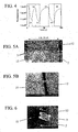
- the figure 4 reports resistance values of a gold film as a function of time when illuminating or extinguishing a halogen lamp whose light is focused on the surface of the gold film. There is a response delay greater than 20 seconds. When the light is on, the measured resistance decreases for a few tens of seconds before starting to stabilize. Similarly, when you turn off the light, it takes a few tens of seconds before the resistance is raised to a level close to the initial level. At least 10, 12 and 15 seconds response delays are measured at the different ignitions, and 10, 20 and 15 seconds at the different extinctions.
- the particles of the device according to the invention have a lower thermal conductivity than gold. Accordingly, if the observed conductance variation in figure 3 was mainly related to a change in temperature, one should observe a delay in the higher response and at least equal to that of gold. Since the response time is faster for the device according to the invention (one to five seconds), this means that the conductance variation presented in FIG. figure 3 is illustrative of the photoconductive properties of the device according to the invention. Such a delay in response represents a fast response time for a photovoltaic or photoconductive device.
- the particles may be randomly present on the surface of the electrodes and only certain particles are simultaneously in direct contact with the two electrodes.
- the Figure 5A is a photograph obtained by scanning electron microscopy of an area of a device according to the invention comprising two electrodes 11, 12, separated by a trench 2 and in which many particles 3 are present on the surface of the electrodes.
- Trench 2 has a width of 70 nm as illustrated by Figure 5B and has a linear distance close to 20 micrometers. For this example, approximately 30 active particles are observed which make it possible to operate the device according to the invention.
- the particles can be positioned almost solely at the trench separating the two electrodes.
- a detail of this preferred mode of the device is illustrated in figure 6 .
- a photograph obtained by scanning electron microscopy of an area of a device according to the invention comprising two electrodes 11, 12, separated by a nanometric trench 2 and comprising five particles 3 which are all in simultaneous contact with the two. electrodes 11, 12, with a higher particle density at the trench than in the embodiment previously described.
- This preferred embodiment of the invention can be obtained by means of a variant of the method according to the invention which will be described below.
- part of the particles used are partially covered with metal, for example a metal film.
- the figure 7 shows a photograph obtained by scanning electron microscopy of such a particle 3. There is observed a particle 3 having a metallized zone 4, lighter, and a non-metallic zone 5, darker.
- the metallized zone 4 may preferentially be in contact with at least one electrode or, alternatively, the non-metallized zone 5 may preferentially be in contact with the electrodes.
- the metallized zone may be gold, nickel or a multilayer gold-nickel structure.
- gold can be replaced by another metal, in particular another metal of the same group: silver, copper, etc. or other metals or their alloys.
- the nickel can be replaced by another metal, for example by another metal or alloy of metals having magnetic properties such as iron or by another metal such as ruthenium.
- the metal may be replaced by a material having particular optical or semiconductor or insulating properties such as silicon or an oxide.
- the active particle 3 in direct simultaneous contact with the two electrodes 11, 12, has a substantially identical electrical contact with the two electrodes.
- the photoelectric device according to the invention then has a substantially identical working function for each electrode and the device behaves like a photoconductor, as reported in FIG. figure 3 .
- a device whose conductance only varies with the light incident on the device can be obtained by the implementation of the first embodiment of the invention.
- a dissymmetry is deliberately introduced between the electrical contact of the particle with one of the two electrodes and the electrical contact of the particle with the other of the two electrodes. It is then formed an asymmetry between the working functions of the two electrodes and such a device according to the second particular embodiment of the invention has photovoltaic properties.
- the device when illuminated by a given light source, it produces in reaction a voltage at its terminals, even in the absence of a current supply. outside the device.
- the voltage depends on the light intensity of the light beam incident on the device from the light source.
- the device can present this property according to two provisions.
- a first provision is to provide a device in which one of the particles has an electrical contact with an electrode such that its access resistance is lower by a factor of 10 to 1000 relative to the other electrode.
- voltage soldering which aims to reduce the lower access resistance between the particle and the electrodes.
- the voltage soldering step only reduces the access resistance of the active particles for only one of the two electrodes.
- the voltage soldering step has operated non-symmetrically.
- the particles (s) then have an "asymmetrical weld" with the two electrodes.
- the device is then a photovoltaic device.
- the dissymmetry is thus obtained without there being any macroscopic structural dissymmetry.
- This asymmetric weld which results in a lower access resistance on one electrode than on the other electrode is interpreted by possible atomic structural differences in the contacts between the particle and the electrodes.
- the observation of a photovoltaic character on a device according to the invention which has no macroscopic structural asymmetry is indicative of a dissymmetry of work function obtained in the manner described above.
- Such photovoltaic devices are obtained randomly, with about ten to thirty percent chance, during the manufacture of photoconductive devices according to the invention. It is therefore preferable to test each device to know which are devices having photovoltaic properties and which are solely photoconductive devices. However, these photovoltaic devices are obtained without complicating the structure or the manufacturing method with respect to the photoconductive devices presented above.
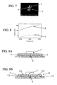
- a prototype of a device according to this second particular embodiment of the invention has been tested and the results of operation are presented in connection with the figure 8 , represents curves I of V (current as a function of a voltage measured at terminals of the device).
- a first measurement was made with a lack of illumination in the room (curve I) and it is observed a curve I of V crossing zero zero origin, zero volts.
- a second current measurement obtained this time under illumination of the device by a light from the halogen lamp and focused on the device is illustrated in curve II.
- This curve does not go through zero ampere origin, zero volt and therefore shows a generation of a current that can reach approximately 100 nA for certain voltage values.
- the current generation by photovoltaic effect is particularly illustrated by the generation of a current close to 75 nanoamperes for an applied voltage of zero volts.
- the trench has a width of about 100 nm and extends over a linear distance close to 5 microns, it can be estimated that the measured current corresponds to a density current close to 8.10 4 Am -2 .
- the active particles are insufficient in number and density.
- the dissymmetry of the electrical contacts is obtained in the particles by an asymmetrical weld which is also a random process.
- the device can be optimized to obtain greater photogeneration.
- a second provision for the device according to the invention to have photovoltaic properties consists in providing a device in which the contact of the electrodes with the particles is made of a metal different from one electrode to the other.
- the surfaces of the two electrodes 11, 12 may be in different metals.
- a dissymmetry of "construction" of the work functions can then be imposed.
- Each electrode may be formed of a single metal as illustrated in FIG. Figure 9A . This metal may be different from one electrode to another or not according to the particular embodiment of the invention used.
- each of the two electrodes has an electrode core 111, 121 of a given metal.
- the metal of the electrode core 111, 121 may be identical or different for the two electrodes 11, 12.
- the metal of the heart electrode 111, 121 may have been chosen to provide another feature to the device.
- each of the electrodes 11, 12 is covered, at least where the particles 3 are in contact with the electrodes 11, 12, by a surface metal layer 112, 122.
- the surface metal layers 112, 122 of the two electrodes can be in the same metal.
- one of the two surface metal layers 112, 122 is made of a first metal and the other of the two surface metal layers 112, 122 is a second metal, different from the first metal according to the particular mode embodiment of the invention used.
- One and / or the other of the two surface metal layers 112, 122 may be in the same metal as the electrode core 111, 121 on which they are respectively.
- the surface metal layers 112, 122 of the electrodes may be of any metal, such as, for example, silver, gold, copper, nickel, aluminum, etc.
- the tests carried out and illustrated in connection with the figures 3 and 8 were made with electrodes whose surface is gold, or a multilayer structure of gold and nickel. It is also possible to obtain a photovoltaic device according to the second particular embodiment of the invention with two electrodes, one of which has a gold surface layer 112 and the other has a metal surface layer 122 of aluminum.
- an advantageous mode consists, independently of the nature of the surface of the electrodes, in providing the cores of the electrodes in a magnetic or magnetizable material. This may in particular be nickel or another magnetic or magnetizable metal or metal alloy.
- the figure 10 is a schematic view of a test bench used to measure the performance of photoelectric devices according to different embodiments of the invention.
- a prototype device according to the invention comprising two electrodes 11, 12 connected by tabs 101i to contacts 102i present on the test bench.
- wires connecting the contacts to external current leads are observed.
- the device according to the invention can be produced with a single active particle or with several active particles per device.
- the particles presented in this description are mainly particles of nanometric size, for example between 30 nm and 700 nm, but the device according to the invention can be produced with particles of larger size. Consequently, the invention is not limited to particles of nanometric size.
- the invention also relates to a method for producing the devices according to the invention.
- a substrate 7 having on the surface two electrodes 11, 12 separated by a trench 2 ( figure 11A ).
- Particles 3 are then deposited on the device at trench 2 ( Figure 11B ).
- the particles 3 are advantageously suspended in a liquid solution.
- the liquid solution comprising the particles 3 is therefore deposited, for example in the form of a localized application of a drop 6 on the device, at the level of the trench 2.
- the liquid solution is then evaporated ( figure 11C ), for example by means of a heat treatment H, which leads to putting the particles 3 in direct contact with the surface of the device.
- a heat treatment H which leads to putting the particles 3 in direct contact with the surface of the device.
- at least one particle 3 is deposited in direct simultaneous contact with the two electrodes 11, 12.
- the particles 3 are retained on the surface of the electrodes, after evaporation of the liquid solution, by physisorption or chemisorption.
- -NH 2 groups located at the periphery of the particles 3 may interact with atoms present at electrode surfaces.
- functional groups may be added to the surface of the electrodes or to the particles in order to facilitate a chemical bond. These groups may be, for example, ionic groups or hydrogen atoms, or thiol, thioaryl or benzonitrile radicals.
- a soldering step is applied under tension. form of the application of a voltage U between the two electrodes ( figure 12 ).
- the voltage U is adapted to the dimensions of the electrodes and to the number of particles 3 expected between the two electrodes 11, 12.
- the voltage U is calibrated so as to reduce the access resistances between the electrodes 11, 12 and the electrodes. particles 3, while remaining small enough not to destroy the particles 3 or the trench separating the electrodes.
- the voltage U produces a modification of the interface between the particles and the electrodes. This modification changes the electrical contact between the particles and the electrodes and decreases the resistance of access. It reduces, at least for one of the two electrodes, the access resistance by a factor of 10 to 1000 or more.
- a voltage of the order of one or two volts for a few seconds can take place from 0.5 V and can not take place up to about 5 V.
- those skilled in the art will preferably apply a voltage of between 0 , 5 V and 5 V to obtain a voltage weld.
- the figure 13 illustrates the phenomenon of improvement of the conductance obtained by applying the voltage soldering according to this preferred embodiment of the method according to the invention. It is mainly represented by conductance measurement results (in siemens) as a function of time (in seconds) for a device according to the invention starting from a time t 0 .
- conductance measurement results in siemens
- the particles are nanoscale and the electrodes are gold.
- a conductance lower than 4.10 -11 siemens is measured.
- a measurement voltage close to 1.5 V is used.
- time t 100 seconds
- a voltage substantially equal to 2 V is imposed across the device.
- This voltage which implements the voltage soldering step of the method of the invention, also serves as a measurement voltage.
- the conductance increases and reaches a value close to 4.10 -8 siemens, a value 1000 times larger than before the soldering voltage.
- the measurement voltage is reduced to approximately 0.05 V and halogen lamp ignition and extinction cycles are applied.
- the light is focused on the device (called ON / OFF cycles), like the test reported in connection with the figure 3 .
- the conductance variations measured during the ON / OFF cycles are reported in an enlarged manner in the box at the top right of the figure 13 .
- the particles 3 are first suspended in a solution 8 ( figure 14A ).
- the solution may be based on ethanol or any other solvent that does not solubilize the particles and has a good evaporation power, such as diethyl ether, water, etc.
- Solution 8 is subjected to ultrasound F for approximately five minutes so as to ensure good separation of the particles from each other and to avoid aggregation of the particles with each other.
- This solution 8 containing the particles is then deposited on a solid support 9, for example in the form of a drop 81 deposited on a surface of gold, nickel or on the surface of a silicon substrate, etc. ( Figure 14B ).
- the metal or metals constituting the metal layer 144 are preferably those mentioned above in connection with the figure 7 .
- the solid support 9 comprising the particles 3 is again brought into contact with a solution 82, containing no particles, and the assembly is subjected to ultrasound F so as to tear off part of the particles 3 from the solid support 9 ( figure 14E ).
- the contacting of the solid support 9 comprising the particles with the solution 82 can be done by depositing the solution on the solid support, for example in the form of drops, or by immersing the solid support 9 in a container having a certain volume solution 82 or any other appropriate solution. In this way, particles 3 partially covered with a metal film forming a metallized zone 4 are suspended in the solution 82.
- FIGs 15A and 15B are two photographs obtained by scanning electron microscopy representing particles 3 present on a physical support 9.
- the photograph of the figure 15A was made before the metallization step.
- particles 3 and physical support 9 were metallized and ultrasound was applied.
- the presence of dark spots representative of tearing zones 14 is noted, from which partially metallized particles have been torn off and resuspended following the action of ultrasound.
- the particles 3 comprising a metallized zone 4 can be used directly in a device according to the invention for the conductive and / or optical properties of the metal film composing the metallized zone.
- the electrodes can be functionalized so that they chemically react preferentially with the metallized zones or with the non-metallized zones, or with a functional group present on the surface of these said zones. This can be done by applying an oxygen plasma treatment, or a hydrogen plasma, or by grafting functional groups on the surface of the electrodes.
- an oxygen plasma treatment or a hydrogen plasma
- grafting functional groups on the surface of the electrodes.
- organic groups for example, thioaryl, dithioaryl, benzonitrile recognized for their affinity with certain metal surfaces (gold, nickel, ...) on the surface of the electrodes.
- the electrodes 11, 12 form a preferential contact with the metallized zones 4 of the particles.
- a first functionalization treatment of the particles 3 in solution is carried out before the metallization step. Then, after metallization, the metal layer covers the functional groups for the metallized zone 4.
- the functional groups favoring or disadvantageous a bond with the electrodes, are present only on the non-metallized zones 5. For example, to form a organic contact / metal, it may be envisaged to fix functional groups to the substituents of the ligands G of the particles, non-metallized side.
- the amine substituent can be coupled to an aldehyde function in order to graft groups, for example, thioaryl, benzonitrile recognized for their affinity with some metal surfaces (Gold, Nickel, ).
- a second functionalization treatment of the particles is carried out after the metallization step and before removing the particles from the solid support.
- the functionalization treatment is applied only to the metallized zone.
- the functional groups added during the second functionalization treatment are present only on the metallized zone 4 and not on the non-metallized zone 5.
- the choice of the different functional groups, the nature of the particles and the nature of the metals used, may advantageously make it possible to predetermine the manner in which the metallized zones will be positioned relative to the electrodes for a majority particles. Thus, it can be determined whether the metallized area will primarily affect the optical or chemical properties of the device affecting the interaction of the device with external stimuli or electrical properties affecting the electrical contact and the resistance of the device.
- the metallized zone 4 present on the particles 3 comprises at least one magnetic or magnetizable metal layer
- the electrodes 11, 12 both comprise an electrode core 111, 121 of magnetic or magnetizable material.
- the electrode cores may be for example nickel or iron or other magnetizable material.
- One and / or the other of the two electrodes 11, 12 may be covered with a metal surface layer 112, 122 made of a metal different from the electrode core 111, 121 depending on the type of device that is desired achieve.
- the electrodes 11, 12 are magnetized prior to the deposition of the drop 6 containing the particle or particles 3.
- the electrodes 11, 12 it is preferable to subject the electrodes 11, 12 to a magnetic field ( figure 16A ).
- a magnetic field figure 16A
- a preferred method is to subject the metallized zones 4 of the particles 3 in suspension to an imposed magnetic field ( figure 16C ).
- the imposed magnetic field can be obtained by presenting a permanent magnet 15 under the substrate 7 which supports the electrodes 11, 12 and the drop 6 of liquid solution.
- the particles 3, controlled by the permanent magnet 15, the magnetized electrodes and the metallized zone 4 which is magnetizable or which covers them, are preferentially positioned at the level of trench 2.
- the particles 3 are advantageously positioned with their metallized zone positioned opposite to the electrodes. It is also possible, as mentioned above, to introduce functional groups on the particles or on the electrodes so that the metallized zones are preferentially attracted by the electrodes ( figure 16C ' ).
- the magnet 15 creates a magnetic field imposed at the surface of the electrodes 11, 12 and the substrate 7.
- the magnet cores 111, 121 magnetized or magnetizable, modify the local magnetic field by increasing it by relative to the imposed magnetic field.
- the magnetic field is close to the value given alone by the imposed magnetic field.
- the magnetic field gradient attracts the metallized zones 4 of the particles 3.
- the liquid solution is evaporated ( figure 16D ).
- a very large part of the particles initially present in solution are then deposited in direct simultaneous contact with the two electrodes 11, 12.
- the particles 3 are advantageously positioned with their non-metallized zone in contact with the electrodes. It is also possible, as mentioned above, to introduce functional groups on the particles or on the electrodes so that the electrodes are preferably in contact with the metallized zones of the particles ( figure 16D ' ).
- the magnetization of the electrode cores 111, 121 was made before the deposition of the drop of solution comprising the particles in suspension.
- the figure 17 is an image obtained by scanning electron microscopy of a device obtained by applying the advantageous method illustrated by means of the Figures 16A to 16D .
- the electrodes have different heights h.
- a first 11 of the two electrodes may be lower than the second 12 of the two electrodes.
- the fields of application of the devices according to the various embodiments of the invention are numerous, particularly in the field of photovoltaics, in the emerging field of molecular electronics, and more broadly in the field of so-called intelligent materials. namely responding to an external stimulus (temperature, pressure, light).
- the particles of the device according to the invention can be chosen so that they have a spin electronic state transition temperature chosen to correspond to a critical temperature.
- This critical temperature can be indicative of a device fatigue temperature or a temperature from which more photovoltaic power is needed.
- Such a photosensitive device can make it possible to make a photovoltaic device which, under the effect of the heating, would change its electronic state of spin, and thus for example of color, and thus of absorption properties. Then the device is 'self-regulating', namely that it self-limits to avoid for example excessive heating.
- the device according to the invention has been described mainly with particles based on a compound that satisfies the chemical formula ⁇ 1 ⁇ . Comparable results are expected for a device comprising a particle that does not satisfy the chemical formula ⁇ 1 ⁇ but has a temperature controlled spin electronic state transition.
Landscapes
- Physics & Mathematics (AREA)
- Nonlinear Science (AREA)
- Spectroscopy & Molecular Physics (AREA)
- Electromagnetism (AREA)
- General Physics & Mathematics (AREA)
- Optics & Photonics (AREA)
- Photovoltaic Devices (AREA)
- Hybrid Cells (AREA)
- Ceramic Capacitors (AREA)
Claims (16)
- Elektrische Vorrichtung umfassend zwei Elektroden, welche voneinander getrennt sind, dadurch gekennzeichnet, dass mindestens ein Partikel mit einem Zustandsübergang des Elektronenspins, welcher durch die Temperatur gesteuert wird, im direkten Kontakt mit jeder der beiden Elektroden ist, wobei das Partikel vom ionischen Typ ist und ein Übergangsmetall umfasst, das eine kationische Ladung trägt.
- Vorrichtung nach Anspruch 1, wobei das Partikel auf einer Verbindung basiert mit der Formel:
[Fe(G)3](X)n,
worin G ein 1,2,4-Triazol-Ligand ist, welcher einen R-Substituenten an dem Stickstoff-Atom an der 4-Position trägt, bezeichnet als R-Trz;X mindestens ein Anion darstellt;und n so berechnet ist, dass die Elektroneutralität der Formel eingehalten wird. - Vorrichtung nach Anspruch 2, wobei der Substituent R aus der Gruppe bestehend aus Wasserstoff und den Verbindungen H2N-, R1-, HR1N- und R1R2N-ausgewählt ist, worin R1 und R2 Alkylreste sind.
- Vorrichtung nach einem der Ansprüche 1 bis 3, wobei das Partikel ein Nanopartikel ist, das mindestens eine Abmessung zwischen 30 nm und 700 nm aufweist.
- Vorrichtung nach Anspruch 4, wobei das Partikel asymmetrisch durch eine Metallschicht abgedeckt wird.
- Vorrichtung nach einem der Ansprüche 1 bis 5, die geeignet ist, um als photoleitende Vorrichtung betrieben zu werden, wobei die beiden Elektroden mit dem gleichen Metall bedeckt sind.
- Vorrichtung nach einem der Ansprüche 1 bis 6, die geeignet ist, um als photovoltaische Vorrichtung betrieben zu werden, wobei eine der beiden Elektroden mit einem ersten Metall und die andere der beiden Elektroden mit einem zweiten Metall bedeckt ist, welches sich von dem ersten Metall unterscheidet.
- Vorrichtung nach einem der Ansprüche 5 bis 7, wobei das Metall aus einem der Elemente aus der Liste bestehend aus Gold, Nickel und einer mehrschichtigen Gold-Nickel-Schichtstruktur ausgewählt ist.
- Vorrichtung nach einem der Ansprüche 1 bis 8, wobei die Elektroden durch einen Graben voneinander getrennt sind, welcher einen Abstand von weniger als oder im Wesentlichen gleich 100 Nanometer zwischen den beiden Elektroden festlegt.
- Vorrichtung nach einem der Ansprüche 1 bis 9, wobei die Elektroden durch einen Graben voneinander getrennt sind und gegenüberliegend mit einem linearen Abstand zwischen einigen Mikrometern und einigen Metern eingestellt werden.
- Vorrichtung nach einem der Ansprüche 1 bis 10, wobei die beiden Elektroden unterschiedliche Höhen aufweisen, die senkrecht zu einer gemeinsamen Hauptebene der beiden Elektroden definiert werden.
- Vorrichtung nach einem der Ansprüche 1 bis 11, die geeignet ist, um als eine photoelektrische Vorrichtung betrieben zu werden, und die in der Lage ist, photoelektrische Eigenschaften ausgehend von einer vorbestimmten Temperatur zu verändern, wobei die Partikel mit einem Zustandsübergang des Elektronenspins aus Partikeln mit einem Zustandsübergang des Elektronenspins ausgewählt sind, der durch die Temperatur gesteuert wird, wobei der Zustandsübergang des Elektronenspins bei der angegebenen Temperatur herum erfolgt.
- Verfahren zur Herstellung einer Vorrichtung nach einem der vorhergehenden Ansprüche, umfassend die aufeinander folgenden folgenden Schritte:a) Bereitstellen von zwei Metallelektroden auf einem Substrat, die voneinander durch einen Graben getrennt sind,b) Ablagern von mindestens einem Partikel mit einem Zustandsübergang des Elektronenspins, welcher durch die Temperatur gesteuert wird, sodass es im gleichzeitigen Kontakt mit den beiden Elektroden liegt, in Form einer lokalisierten Abscheidung einer flüssigen Lösung, umfassend das Partikel in ionischer Lösung, gefolgt von einer Verdampfung der flüssigen Lösung, die das Partikel auf der Vorrichtung lässt, wobei das Partikel vom ionischen Typ ist, umfassend ein Übergangsmetall, das eine kationische Ladung trägt, wobei die Elektroneutralität der flüssigen Lösung durch ein anionisches Gegenion gewährleistet wird.
- Verfahren nach Anspruch 13, umfassend, nach dem Schritt b), das Anlegen einer Spannung zwischen den beiden Elektroden, die hoch genug ist, um die Zugangswiderstände zwischen den Elektroden und dem Partikel zu reduzieren, aber die niedrig genug ist, um die Zerstörung des Partikels oder des Grabens, welcher die Elektroden trennt, zu vermeiden.
- Verfahren nach Anspruch 14, wobei die angelegte Spannung zwischen 0,5 Volt und 5 Volt liegt.
- Verfahren nach einem der Ansprüche 13 bis 15, wobei die Elektroden mindestens ein magnetisierbares Metall umfassen, und wobei vor dem Schritt b) vorgesehen ist:- ein Schritt, in welchem das in Schritt b) abzulagernde Partikel teilweise mit einer Metallschicht abgedeckt wird, die magnetische Eigenschaften aufweist,- und ein Schritt der Magnetisierung der Elektroden durch Anlegen eines Magnetfeldes auf Höhe der beiden Elektroden,- und wobei der Schritt b) zwischen der Abscheidung der flüssigen Lösung und ihrer Verdampfung einen Schritt zur Anordnung der Partikel auf dem Graben, welcher die Elektroden trennt, mittels einer Anwendung eines Magnetfeldes auf Höhe der beiden Elektroden umfasst.
Applications Claiming Priority (2)
| Application Number | Priority Date | Filing Date | Title |
|---|---|---|---|
| FR1150949A FR2971364B1 (fr) | 2011-02-07 | 2011-02-07 | Agencement optimise de particules de triazole |
| PCT/FR2012/050259 WO2012107680A1 (fr) | 2011-02-07 | 2012-02-07 | Agencement optimisé de particules de triazole |
Publications (2)
| Publication Number | Publication Date |
|---|---|
| EP2673817A1 EP2673817A1 (de) | 2013-12-18 |
| EP2673817B1 true EP2673817B1 (de) | 2015-04-15 |
Family
ID=44501663
Family Applications (1)
| Application Number | Title | Priority Date | Filing Date |
|---|---|---|---|
| EP12707875.6A Not-in-force EP2673817B1 (de) | 2011-02-07 | 2012-02-07 | Optimierte anordnung von triazolpartikeln |
Country Status (6)
| Country | Link |
|---|---|
| US (1) | US9594264B2 (de) |
| EP (1) | EP2673817B1 (de) |
| JP (1) | JP5968918B2 (de) |
| CN (1) | CN103460425B (de) |
| FR (1) | FR2971364B1 (de) |
| WO (1) | WO2012107680A1 (de) |
Cited By (1)
| Publication number | Priority date | Publication date | Assignee | Title |
|---|---|---|---|---|
| JP2014507068A (ja) * | 2011-02-07 | 2014-03-20 | サントル・ナショナル・ドゥ・ラ・レシェルシュ・サイエンティフィーク−セ・エン・エール・エス− | 最適化されたトリアゾール粒子配置 |
Families Citing this family (1)
| Publication number | Priority date | Publication date | Assignee | Title |
|---|---|---|---|---|
| FR3020719A1 (fr) * | 2014-05-05 | 2015-11-06 | Centre Nat Rech Scient | Dispositif muni d'une paire d'electrodes et d'au moins une particule a transition d'etat de spin au contact des electrodes, procede de fabrication associe et differentes utilisations de ce dispositif. |
Family Cites Families (14)
| Publication number | Priority date | Publication date | Assignee | Title |
|---|---|---|---|---|
| JPS6313381A (ja) * | 1986-07-03 | 1988-01-20 | Nok Corp | 光電センサ |
| US6200730B1 (en) * | 1992-11-20 | 2001-03-13 | U.S. Philips Corporation | Spin-transition parent compounds |
| FR2755697A1 (fr) | 1996-11-14 | 1998-05-15 | Philips Electronics Nv | Composes chimiques a transition de spin et dispositifs d'affichage de depassement de seuil de temperature comprenant un milieu actif incluant au moins un de ces composes |
| TW555790B (en) * | 2000-12-26 | 2003-10-01 | Matsushita Electric Industrial Co Ltd | Conductive organic thin film, process for producing the same, and organic photoelectronic device, electric wire, and electrode aech employing the same |
| KR100492482B1 (ko) * | 2002-09-04 | 2005-06-03 | 한국과학기술연구원 | Pembe로 제조된 상온 자성반도체 및 그 소자 |
| KR100861522B1 (ko) * | 2003-12-26 | 2008-10-02 | 후지제롯쿠스 가부시끼가이샤 | 정류 소자 및 그것을 사용한 전자 회로, 및 정류 소자의제조 방법 |
| JP5066918B2 (ja) * | 2004-12-28 | 2012-11-07 | 日本電気株式会社 | スイッチング素子、書き換え可能な論理集積回路、およびメモリ素子 |
| FR2894581B1 (fr) * | 2005-12-08 | 2008-02-22 | Centre Nat Rech Scient | Nanoparticules d'un compose a transition de spin |
| US7625767B2 (en) * | 2006-03-17 | 2009-12-01 | Mears Technologies, Inc. | Methods of making spintronic devices with constrained spintronic dopant |
| US7923801B2 (en) * | 2007-04-18 | 2011-04-12 | Invisage Technologies, Inc. | Materials, systems and methods for optoelectronic devices |
| FR2917410B1 (fr) * | 2007-06-12 | 2012-09-07 | Centre Nat Rech Scient | Compose a transition de spin. |
| KR20090013657A (ko) * | 2007-08-02 | 2009-02-05 | 한국전자통신연구원 | Ge기반 금속-절연체 전이(MIT) 박막, 그 MIT박막을 포함하는 MIT 소자 및 그 MIT 소자 제조방법 |
| JP2009212164A (ja) * | 2008-02-29 | 2009-09-17 | Univ Of Tokyo | 電子素子、ディスプレイ装置、記憶素子、光センサ、ガスセンサ及び電子素子製造方法 |
| FR2971364B1 (fr) * | 2011-02-07 | 2013-02-15 | Centre Nat Rech Scient | Agencement optimise de particules de triazole |
-
2011
- 2011-02-07 FR FR1150949A patent/FR2971364B1/fr not_active Expired - Fee Related
-
2012
- 2012-02-07 WO PCT/FR2012/050259 patent/WO2012107680A1/fr not_active Ceased
- 2012-02-07 JP JP2013552249A patent/JP5968918B2/ja not_active Expired - Fee Related
- 2012-02-07 US US13/983,122 patent/US9594264B2/en not_active Expired - Fee Related
- 2012-02-07 EP EP12707875.6A patent/EP2673817B1/de not_active Not-in-force
- 2012-02-07 CN CN201280014478.9A patent/CN103460425B/zh not_active Expired - Fee Related
Cited By (1)
| Publication number | Priority date | Publication date | Assignee | Title |
|---|---|---|---|---|
| JP2014507068A (ja) * | 2011-02-07 | 2014-03-20 | サントル・ナショナル・ドゥ・ラ・レシェルシュ・サイエンティフィーク−セ・エン・エール・エス− | 最適化されたトリアゾール粒子配置 |
Also Published As
| Publication number | Publication date |
|---|---|
| EP2673817A1 (de) | 2013-12-18 |
| FR2971364A1 (fr) | 2012-08-10 |
| WO2012107680A1 (fr) | 2012-08-16 |
| US20130306936A1 (en) | 2013-11-21 |
| FR2971364B1 (fr) | 2013-02-15 |
| JP5968918B2 (ja) | 2016-08-10 |
| CN103460425B (zh) | 2016-10-05 |
| JP2014507068A (ja) | 2014-03-20 |
| CN103460425A (zh) | 2013-12-18 |
| US9594264B2 (en) | 2017-03-14 |
Similar Documents
| Publication | Publication Date | Title |
|---|---|---|
| EP2339658A2 (de) | Herstellungsverfahren einer Elektrode mit isolierenden und metalischen Nanostrukturen zum Farbfiltern in einer OLED und Herstellungsverfahren einer OLED | |
| FR2830971A1 (fr) | Dispositif magnetoresistif a vanne de spin a performances ameliorees | |
| Song et al. | Hole transfer from single quantum dots | |
| CH343534A (fr) | Redresseur électrique à cristal | |
| EP2673817B1 (de) | Optimierte anordnung von triazolpartikeln | |
| KR20220139721A (ko) | 플라즈모닉 하이브리드 나노입자, 이산화티타늄 및 그래핀 양자점을 포함하는 uv 광검출기용 기판 및 이를 이용하는 uv 광검출기 | |
| FR3045826A1 (fr) | Supports amplificateurs de contraste utilisant un materiau bidimensionnel | |
| FR2771511A1 (fr) | Capteur de champ magnetique et procede de fabrication de ce capteur | |
| FR2596921A1 (fr) | Procede de formation d'un dessin conducteur sur la surface d'un semi-conducteur tel que notamment du silicium, germanium et l'arsenium de gallium | |
| Naddaf et al. | Characterization of nanostructured CuO–porous silicon matrix formed on copper-coated silicon substrate via electrochemical etching | |
| Frydendahl et al. | hBN‐Encapsulated Graphene Coupled to a Plasmonic Metasurface via 1D Electrodes for Photodetection Applications | |
| FR2509063A1 (fr) | Ensemble photoconducteur a couches multiples avec une heterojonction intermediaire | |
| FR2873493A1 (fr) | Dispositif semiconducteur a nanotube ou nanofil, configurable optiquement | |
| Akbıyık et al. | Laser Photochemical Nanostructuring of Silicon for Surface Enhanced Raman Spectroscopy | |
| EP2633566B1 (de) | Elektrische leitung mittels supramolekularer anordnungen aus triarylaminen | |
| FR2987131A1 (fr) | Sonde active pour microscopie optique en champ proche et son procede de fabrication. | |
| EP1547136B1 (de) | Verfahren zur herstellung einer drahtförmigen nanostruktur aus einer halbleitenden schicht | |
| FR2758431A1 (fr) | Dispositif d'affichage electroluminescent en couche mince et a excitation alternative et son procede de realisation | |
| Zhao et al. | Polarized Single‐Pixel Imaging System Based on Patterned Quantum Dot Film: Synergistic Effect of Periodical Dielectric Field and Carrier Movement Anisotropy | |
| Iatsunskyi et al. | Peculiarities of Photoluminescence in Porous Silicon Prepared by Metal‐Assisted Chemical Etching | |
| Khalili et al. | Study of anodization parameters effects on photoconductivity of porous silicon | |
| EP2596523A1 (de) | Vorrichtung und verfahren zur herstellung auf einem halbleiternanodraht einer legierung dieses halbleiters mit einem metall oder metalloid | |
| Teoh et al. | Dye-improved optical absorption of vertically aligned silicon nanowire arrays synthesized by electroless etching of silicon wafer | |
| Rashid et al. | Performance of SiQDs and H_Si nanopillars/etched Si electrical sensor synthesized by aggressive laser-assisted etching method: comparative study: RB Rashid et al. | |
| Zhang et al. | Optothermal Formation of Gold “Nano‐Lemons” for SERS on Photolipid Bilayer Membranes |
Legal Events
| Date | Code | Title | Description |
|---|---|---|---|
| PUAI | Public reference made under article 153(3) epc to a published international application that has entered the european phase |
Free format text: ORIGINAL CODE: 0009012 |
|
| 17P | Request for examination filed |
Effective date: 20130723 |
|
| AK | Designated contracting states |
Kind code of ref document: A1 Designated state(s): AL AT BE BG CH CY CZ DE DK EE ES FI FR GB GR HR HU IE IS IT LI LT LU LV MC MK MT NL NO PL PT RO RS SE SI SK SM TR |
|
| DAX | Request for extension of the european patent (deleted) | ||
| GRAP | Despatch of communication of intention to grant a patent |
Free format text: ORIGINAL CODE: EPIDOSNIGR1 |
|
| RIC1 | Information provided on ipc code assigned before grant |
Ipc: G02F 1/00 20060101ALI20141111BHEP Ipc: H01L 51/05 20060101ALI20141111BHEP Ipc: G02F 1/01 20060101ALI20141111BHEP Ipc: H01L 51/42 20060101AFI20141111BHEP |
|
| INTG | Intention to grant announced |
Effective date: 20141202 |
|
| GRAS | Grant fee paid |
Free format text: ORIGINAL CODE: EPIDOSNIGR3 |
|
| GRAA | (expected) grant |
Free format text: ORIGINAL CODE: 0009210 |
|
| AK | Designated contracting states |
Kind code of ref document: B1 Designated state(s): AL AT BE BG CH CY CZ DE DK EE ES FI FR GB GR HR HU IE IS IT LI LT LU LV MC MK MT NL NO PL PT RO RS SE SI SK SM TR |
|
| REG | Reference to a national code |
Ref country code: GB Ref legal event code: FG4D Free format text: NOT ENGLISH Ref country code: CH Ref legal event code: EP |
|
| REG | Reference to a national code |
Ref country code: IE Ref legal event code: FG4D Free format text: LANGUAGE OF EP DOCUMENT: FRENCH |
|
| REG | Reference to a national code |
Ref country code: AT Ref legal event code: REF Ref document number: 722401 Country of ref document: AT Kind code of ref document: T Effective date: 20150515 |
|
| REG | Reference to a national code |
Ref country code: DE Ref legal event code: R096 Ref document number: 602012006716 Country of ref document: DE Effective date: 20150528 |
|
| REG | Reference to a national code |
Ref country code: NL Ref legal event code: T3 |
|
| REG | Reference to a national code |
Ref country code: NL Ref legal event code: T3 |
|
| REG | Reference to a national code |
Ref country code: AT Ref legal event code: MK05 Ref document number: 722401 Country of ref document: AT Kind code of ref document: T Effective date: 20150415 |
|
| REG | Reference to a national code |
Ref country code: LT Ref legal event code: MG4D |
|
| PG25 | Lapsed in a contracting state [announced via postgrant information from national office to epo] |
Ref country code: FI Free format text: LAPSE BECAUSE OF FAILURE TO SUBMIT A TRANSLATION OF THE DESCRIPTION OR TO PAY THE FEE WITHIN THE PRESCRIBED TIME-LIMIT Effective date: 20150415 Ref country code: PT Free format text: LAPSE BECAUSE OF FAILURE TO SUBMIT A TRANSLATION OF THE DESCRIPTION OR TO PAY THE FEE WITHIN THE PRESCRIBED TIME-LIMIT Effective date: 20150817 Ref country code: HR Free format text: LAPSE BECAUSE OF FAILURE TO SUBMIT A TRANSLATION OF THE DESCRIPTION OR TO PAY THE FEE WITHIN THE PRESCRIBED TIME-LIMIT Effective date: 20150415 Ref country code: LT Free format text: LAPSE BECAUSE OF FAILURE TO SUBMIT A TRANSLATION OF THE DESCRIPTION OR TO PAY THE FEE WITHIN THE PRESCRIBED TIME-LIMIT Effective date: 20150415 Ref country code: ES Free format text: LAPSE BECAUSE OF FAILURE TO SUBMIT A TRANSLATION OF THE DESCRIPTION OR TO PAY THE FEE WITHIN THE PRESCRIBED TIME-LIMIT Effective date: 20150415 Ref country code: NO Free format text: LAPSE BECAUSE OF FAILURE TO SUBMIT A TRANSLATION OF THE DESCRIPTION OR TO PAY THE FEE WITHIN THE PRESCRIBED TIME-LIMIT Effective date: 20150715 |
|
| PG25 | Lapsed in a contracting state [announced via postgrant information from national office to epo] |
Ref country code: IS Free format text: LAPSE BECAUSE OF FAILURE TO SUBMIT A TRANSLATION OF THE DESCRIPTION OR TO PAY THE FEE WITHIN THE PRESCRIBED TIME-LIMIT Effective date: 20150815 Ref country code: GR Free format text: LAPSE BECAUSE OF FAILURE TO SUBMIT A TRANSLATION OF THE DESCRIPTION OR TO PAY THE FEE WITHIN THE PRESCRIBED TIME-LIMIT Effective date: 20150716 Ref country code: LV Free format text: LAPSE BECAUSE OF FAILURE TO SUBMIT A TRANSLATION OF THE DESCRIPTION OR TO PAY THE FEE WITHIN THE PRESCRIBED TIME-LIMIT Effective date: 20150415 Ref country code: RS Free format text: LAPSE BECAUSE OF FAILURE TO SUBMIT A TRANSLATION OF THE DESCRIPTION OR TO PAY THE FEE WITHIN THE PRESCRIBED TIME-LIMIT Effective date: 20150415 Ref country code: AT Free format text: LAPSE BECAUSE OF FAILURE TO SUBMIT A TRANSLATION OF THE DESCRIPTION OR TO PAY THE FEE WITHIN THE PRESCRIBED TIME-LIMIT Effective date: 20150415 |
|
| REG | Reference to a national code |
Ref country code: DE Ref legal event code: R097 Ref document number: 602012006716 Country of ref document: DE |
|
| REG | Reference to a national code |
Ref country code: FR Ref legal event code: PLFP Year of fee payment: 5 |
|
| PG25 | Lapsed in a contracting state [announced via postgrant information from national office to epo] |
Ref country code: EE Free format text: LAPSE BECAUSE OF FAILURE TO SUBMIT A TRANSLATION OF THE DESCRIPTION OR TO PAY THE FEE WITHIN THE PRESCRIBED TIME-LIMIT Effective date: 20150415 Ref country code: DK Free format text: LAPSE BECAUSE OF FAILURE TO SUBMIT A TRANSLATION OF THE DESCRIPTION OR TO PAY THE FEE WITHIN THE PRESCRIBED TIME-LIMIT Effective date: 20150415 |
|
| PLBE | No opposition filed within time limit |
Free format text: ORIGINAL CODE: 0009261 |
|
| STAA | Information on the status of an ep patent application or granted ep patent |
Free format text: STATUS: NO OPPOSITION FILED WITHIN TIME LIMIT |
|
| PG25 | Lapsed in a contracting state [announced via postgrant information from national office to epo] |
Ref country code: RO Free format text: LAPSE BECAUSE OF NON-PAYMENT OF DUE FEES Effective date: 20150415 Ref country code: SK Free format text: LAPSE BECAUSE OF FAILURE TO SUBMIT A TRANSLATION OF THE DESCRIPTION OR TO PAY THE FEE WITHIN THE PRESCRIBED TIME-LIMIT Effective date: 20150415 Ref country code: PL Free format text: LAPSE BECAUSE OF FAILURE TO SUBMIT A TRANSLATION OF THE DESCRIPTION OR TO PAY THE FEE WITHIN THE PRESCRIBED TIME-LIMIT Effective date: 20150415 Ref country code: CZ Free format text: LAPSE BECAUSE OF FAILURE TO SUBMIT A TRANSLATION OF THE DESCRIPTION OR TO PAY THE FEE WITHIN THE PRESCRIBED TIME-LIMIT Effective date: 20150415 |
|
| 26N | No opposition filed |
Effective date: 20160118 |
|
| PG25 | Lapsed in a contracting state [announced via postgrant information from national office to epo] |
Ref country code: IT Free format text: LAPSE BECAUSE OF FAILURE TO SUBMIT A TRANSLATION OF THE DESCRIPTION OR TO PAY THE FEE WITHIN THE PRESCRIBED TIME-LIMIT Effective date: 20150415 |
|
| PG25 | Lapsed in a contracting state [announced via postgrant information from national office to epo] |
Ref country code: SI Free format text: LAPSE BECAUSE OF FAILURE TO SUBMIT A TRANSLATION OF THE DESCRIPTION OR TO PAY THE FEE WITHIN THE PRESCRIBED TIME-LIMIT Effective date: 20150415 |
|
| PG25 | Lapsed in a contracting state [announced via postgrant information from national office to epo] |
Ref country code: MC Free format text: LAPSE BECAUSE OF FAILURE TO SUBMIT A TRANSLATION OF THE DESCRIPTION OR TO PAY THE FEE WITHIN THE PRESCRIBED TIME-LIMIT Effective date: 20150415 Ref country code: LU Free format text: LAPSE BECAUSE OF FAILURE TO SUBMIT A TRANSLATION OF THE DESCRIPTION OR TO PAY THE FEE WITHIN THE PRESCRIBED TIME-LIMIT Effective date: 20160207 |
|
| REG | Reference to a national code |
Ref country code: IE Ref legal event code: MM4A |
|
| REG | Reference to a national code |
Ref country code: FR Ref legal event code: PLFP Year of fee payment: 6 |
|
| PG25 | Lapsed in a contracting state [announced via postgrant information from national office to epo] |
Ref country code: IE Free format text: LAPSE BECAUSE OF NON-PAYMENT OF DUE FEES Effective date: 20160207 |
|
| PG25 | Lapsed in a contracting state [announced via postgrant information from national office to epo] |
Ref country code: SE Free format text: LAPSE BECAUSE OF FAILURE TO SUBMIT A TRANSLATION OF THE DESCRIPTION OR TO PAY THE FEE WITHIN THE PRESCRIBED TIME-LIMIT Effective date: 20150415 |
|
| PG25 | Lapsed in a contracting state [announced via postgrant information from national office to epo] |
Ref country code: MT Free format text: LAPSE BECAUSE OF FAILURE TO SUBMIT A TRANSLATION OF THE DESCRIPTION OR TO PAY THE FEE WITHIN THE PRESCRIBED TIME-LIMIT Effective date: 20150415 |
|
| REG | Reference to a national code |
Ref country code: FR Ref legal event code: PLFP Year of fee payment: 7 |
|
| PG25 | Lapsed in a contracting state [announced via postgrant information from national office to epo] |
Ref country code: SM Free format text: LAPSE BECAUSE OF FAILURE TO SUBMIT A TRANSLATION OF THE DESCRIPTION OR TO PAY THE FEE WITHIN THE PRESCRIBED TIME-LIMIT Effective date: 20150415 Ref country code: CY Free format text: LAPSE BECAUSE OF FAILURE TO SUBMIT A TRANSLATION OF THE DESCRIPTION OR TO PAY THE FEE WITHIN THE PRESCRIBED TIME-LIMIT Effective date: 20150415 Ref country code: HU Free format text: LAPSE BECAUSE OF FAILURE TO SUBMIT A TRANSLATION OF THE DESCRIPTION OR TO PAY THE FEE WITHIN THE PRESCRIBED TIME-LIMIT; INVALID AB INITIO Effective date: 20120207 |
|
| PG25 | Lapsed in a contracting state [announced via postgrant information from national office to epo] |
Ref country code: TR Free format text: LAPSE BECAUSE OF FAILURE TO SUBMIT A TRANSLATION OF THE DESCRIPTION OR TO PAY THE FEE WITHIN THE PRESCRIBED TIME-LIMIT Effective date: 20150415 Ref country code: MK Free format text: LAPSE BECAUSE OF FAILURE TO SUBMIT A TRANSLATION OF THE DESCRIPTION OR TO PAY THE FEE WITHIN THE PRESCRIBED TIME-LIMIT Effective date: 20150415 |
|
| PG25 | Lapsed in a contracting state [announced via postgrant information from national office to epo] |
Ref country code: BG Free format text: LAPSE BECAUSE OF FAILURE TO SUBMIT A TRANSLATION OF THE DESCRIPTION OR TO PAY THE FEE WITHIN THE PRESCRIBED TIME-LIMIT Effective date: 20150415 |
|
| PG25 | Lapsed in a contracting state [announced via postgrant information from national office to epo] |
Ref country code: AL Free format text: LAPSE BECAUSE OF FAILURE TO SUBMIT A TRANSLATION OF THE DESCRIPTION OR TO PAY THE FEE WITHIN THE PRESCRIBED TIME-LIMIT Effective date: 20150415 |
|
| PGFP | Annual fee paid to national office [announced via postgrant information from national office to epo] |
Ref country code: DE Payment date: 20190211 Year of fee payment: 8 Ref country code: GB Payment date: 20190215 Year of fee payment: 8 Ref country code: CH Payment date: 20190218 Year of fee payment: 8 Ref country code: NL Payment date: 20190115 Year of fee payment: 8 |
|
| PGFP | Annual fee paid to national office [announced via postgrant information from national office to epo] |
Ref country code: BE Payment date: 20190222 Year of fee payment: 8 Ref country code: FR Payment date: 20190228 Year of fee payment: 8 |
|
| REG | Reference to a national code |
Ref country code: DE Ref legal event code: R119 Ref document number: 602012006716 Country of ref document: DE |
|
| REG | Reference to a national code |
Ref country code: CH Ref legal event code: PL |
|
| REG | Reference to a national code |
Ref country code: NL Ref legal event code: MM Effective date: 20200301 |
|
| GBPC | Gb: european patent ceased through non-payment of renewal fee |
Effective date: 20200207 |
|
| REG | Reference to a national code |
Ref country code: BE Ref legal event code: MM Effective date: 20200229 |
|
| PG25 | Lapsed in a contracting state [announced via postgrant information from national office to epo] |
Ref country code: LI Free format text: LAPSE BECAUSE OF NON-PAYMENT OF DUE FEES Effective date: 20200229 Ref country code: CH Free format text: LAPSE BECAUSE OF NON-PAYMENT OF DUE FEES Effective date: 20200229 |
|
| PG25 | Lapsed in a contracting state [announced via postgrant information from national office to epo] |
Ref country code: NL Free format text: LAPSE BECAUSE OF NON-PAYMENT OF DUE FEES Effective date: 20200301 |
|
| PG25 | Lapsed in a contracting state [announced via postgrant information from national office to epo] |
Ref country code: DE Free format text: LAPSE BECAUSE OF NON-PAYMENT OF DUE FEES Effective date: 20200901 Ref country code: FR Free format text: LAPSE BECAUSE OF NON-PAYMENT OF DUE FEES Effective date: 20200229 Ref country code: GB Free format text: LAPSE BECAUSE OF NON-PAYMENT OF DUE FEES Effective date: 20200207 |
|
| PG25 | Lapsed in a contracting state [announced via postgrant information from national office to epo] |
Ref country code: BE Free format text: LAPSE BECAUSE OF NON-PAYMENT OF DUE FEES Effective date: 20200229 |