EP2674949B1 - PTC-Vorrichtung mit Gehäuse mit elektrischen Abschaltmitteln im Fehlerfall - Google Patents
PTC-Vorrichtung mit Gehäuse mit elektrischen Abschaltmitteln im Fehlerfall Download PDFInfo
- Publication number
- EP2674949B1 EP2674949B1 EP13172159.9A EP13172159A EP2674949B1 EP 2674949 B1 EP2674949 B1 EP 2674949B1 EP 13172159 A EP13172159 A EP 13172159A EP 2674949 B1 EP2674949 B1 EP 2674949B1
- Authority
- EP
- European Patent Office
- Prior art keywords
- support
- contact part
- elastic
- electrode
- electronic element
- Prior art date
- Legal status (The legal status is an assumption and is not a legal conclusion. Google has not performed a legal analysis and makes no representation as to the accuracy of the status listed.)
- Not-in-force
Links
- 239000012634 fragment Substances 0.000 claims description 27
- 239000000463 material Substances 0.000 description 8
- 238000007599 discharging Methods 0.000 description 6
- 238000013021 overheating Methods 0.000 description 6
- 239000004065 semiconductor Substances 0.000 description 4
- 239000000919 ceramic Substances 0.000 description 3
- 230000006835 compression Effects 0.000 description 3
- 238000007906 compression Methods 0.000 description 3
- 102100028680 Protein patched homolog 1 Human genes 0.000 description 1
- 101710161390 Protein patched homolog 1 Proteins 0.000 description 1
- 102100036894 Protein patched homolog 2 Human genes 0.000 description 1
- 101710161395 Protein patched homolog 2 Proteins 0.000 description 1
- 230000002159 abnormal effect Effects 0.000 description 1
- 230000006378 damage Effects 0.000 description 1
- 238000005516 engineering process Methods 0.000 description 1
- 229920006015 heat resistant resin Polymers 0.000 description 1
- 239000000155 melt Substances 0.000 description 1
- 238000012986 modification Methods 0.000 description 1
- 230000004048 modification Effects 0.000 description 1
- 239000003507 refrigerant Substances 0.000 description 1
- 238000005057 refrigeration Methods 0.000 description 1
- 239000007858 starting material Substances 0.000 description 1
- 229920005992 thermoplastic resin Polymers 0.000 description 1
Images



Classifications
-
- H—ELECTRICITY
- H01—ELECTRIC ELEMENTS
- H01C—RESISTORS
- H01C7/00—Non-adjustable resistors formed as one or more layers or coatings; Non-adjustable resistors made from powdered conducting material or powdered semi-conducting material with or without insulating material
- H01C7/02—Non-adjustable resistors formed as one or more layers or coatings; Non-adjustable resistors made from powdered conducting material or powdered semi-conducting material with or without insulating material having positive temperature coefficient
-
- H—ELECTRICITY
- H01—ELECTRIC ELEMENTS
- H01C—RESISTORS
- H01C1/00—Details
- H01C1/01—Mounting; Supporting
- H01C1/014—Mounting; Supporting the resistor being suspended between and being supported by two supporting sections
-
- H—ELECTRICITY
- H01—ELECTRIC ELEMENTS
- H01C—RESISTORS
- H01C1/00—Details
- H01C1/02—Housing; Enclosing; Embedding; Filling the housing or enclosure
- H01C1/022—Housing; Enclosing; Embedding; Filling the housing or enclosure the housing or enclosure being openable or separable from the resistive element
Definitions
- the present invention relates to an electronic device, in particular, to a positive temperature coefficient (PTC) thermistor device.
- PTC positive temperature coefficient
- Thermistor device has been widely used in current limiting circuit, including motor staring circuit in a refrigeration device such as a refrigerator. After being used for long time, the physical structure of the prior art PTC device may deteriorate, creating abnormal heat inside the device and breaking the PTC element into fragments. Since the fragments may still be connected with the terminal, issues such as arc discharging, overheating, over current, etc. may occur.
- Current conducting contact elements are arranged offset relative to each other on the component.
- At least one positioning element is arranged on the component.
- At least one of the contact elements or the positioning element comprise a tensioned member which is electrically separated from the contact elements.
- At least one contact element and position element pair is arranged on the component such that the principle of the short, i.e. high pressing force, asymmetrical stress on component, and the long, i.e. strong tilting of bridging members after destruction of the component, lever arm is guaranteed.
- German patent application no. DE 19638631 A1 discloses a contact assembly for semiconductor resistors, consisting of a set of contact elements asymmetrically arranged so that they lean, staggered in relation to each other, against the opposite side surfaces of an electrical structural member.
- European patent application no. EP-A-1511053 discloses a motor start relay comprising a positive temperature PTC thermistor, a PTC case of heat resistant resin for receiving the PTC thermistor horizontally, first and second contact/terminals each having contacts electrically engaged with a respective electrode surface of the PTC thermistor in the PTC case, a housing receiving the PTC case and a cover attached on the housing.
- thermistor portion PTC1 is rotated by spring contact (510) with a force F1
- thermistor portion PTC2 is pushed by spring contact (570) at the reverse direction and is dropped through an opening of the PTC case.
- United States patent no. 5,760,676 discloses a positive temperature coefficient thermistor in which a terminal holding member is provided between an outer casing and an elastic terminal electrically connected to the semiconductor ceramic element.
- the terminal holding member is formed of a thermoplastic resin having a low softening point. Consequently, when an abnormally large amount of heat is generated in the semiconductor ceramic element, the terminal holding member melts and deforms, causing the semiconductor ceramic element to be separated and thereby electrically disconnected from the terminal.
- current thermistor device may not be able to reliably eliminate the issues of arc discharging and overheating in a failure broken state.
- the present disclosure presents an electronic device as defined in claim 1 which includes: an electronic element with a first electrode and a second electrode disposed on the opposite sides thereof; a first terminal and a second terminal; a first support mounted to and electrically connected with the first terminal, the first support comprising a first contact part contacting and electrically connected with the first electrode; a second support mounted to and electrically connected with the second terminal, the second support comprising a second contact part contacting and electrically connected with the second electrode; a third elastic support comprising a third contact part contacting with one of the first electrode and the second electrode, wherein the third elastic support is provided so as to push a first and a separate second fragment of the electronic element out of contact with one of the first support and the second support when the electronic element breaks in a failure state.
- the elastic force of the third elastic support pushes the fragments of the electronic element away so that the fragments do not contact with one of the first support and the second support, disconnecting the electronic element with one of the terminals, disconnecting the circuit and eliminating the issues of arc discharging and overheating.
- the third elastic support may be electrically insulated with said one of the first support and the second support as well as the terminal electrically connected therewith, when the electronic element breaks in a failure state.
- Said one of the first support and the second support may be a rigid support.
- the second support may be a rigid support, and the third contact part contacts with the second electrode at a position close to the second contact part.
- the third elastic support may comprise a first elastic part providing the third contact part and a second elastic part including a forth contact part contacting with the second electrode at a position different from the second contact part and the third contact part .
- the first contact part may be closer to the center of the electronic element than the second contact part and the forth contact part, and the second contact part and the forth contact part may be opposite to each other across the first contact part.
- the second elastic part may apply a second elastic force on the electronic element
- the first elastic part may apply a first elastic force on the electronic element
- the second elastic force may be greater than the first elastic force
- the electronic device may be such that fragments of the electronic element are pushed away from the second support by the first elastic force when the electronic element breaks in a failure state, so that the second support is out of contact with the second electrode.
- the first support may apply a force toward the first electrode and the second support may apply a force toward the second electrode due to the first elastic force and the second elastic force, so that the first support keeps close contact with the first electrode and the second support keeps close contact with the second electrode.
- the first elastic part may comprise two elastic forks, the second contact part being positioned between the two forks and spaced therewith.
- An elastic force on the electronic element applied by the second elastic part may be greater than the sum of the elastic force on the electronic element applied by the two forks.
- the second contact part may be spaced from the two forks in a direction crossing a line connecting the second contact part with the forth contact part.
- the spaced distance between the second contact part and the two forks may be less than 2mm.
- the first contact part may be positioned at the center of the electronic element, and a line connecting the second contact part and the forth contact part may pass the center of the electronic element.
- the electronic element may be a PTC disc.
- the first support may be integral with the first terminal.
- the second support may be integral with the second terminal.
- the electronic device may further include a forth elastic support with a forth contact part contacting the second electrode at a position different with the second contact part and the third contact part.
- the first contact part may be closer to the center of the electronic element than the second contact part and the forth contact part, and the second contact part and the forth contact part may be opposite to each other across the first contact part.
- the forth elastic part may apply a second elastic force on the electronic element
- the third elastic part may apply a first elastic force on the electronic element
- the second elastic force may be greater than the first elastic force
- the electronic device may be such that fragments of the electronic element are pushed away from the second support by the first elastic force when the electronic element breaks in a failure state, so that the second support is out of contact with the second electrode.
- the first support may apply a force toward a first electrode and the second support may apply a force toward a second electrode due to the first elastic force and the second elastic force, so that the first support keeps close contact with the first electrode and the second support keeps close contact with the second electrode.
- the third elastic part may comprise two elastic forks, the second contact part being positioned between the two forks and spaced therewith.
- the elastic force on the electronic element applied by the forth elastic part may be greater than the sum of the elastic force on the electronic element applied by the two forks.
- the second contact part may be spaced from the two forks in a direction crossing a line connecting the second contact part with the forth contact part.
- the spaced distance between the second contact part and the two forks may be less than 2mm.
- the first contact part may be positioned at the center of the electronic element, and a line connecting the second contact part and the forth contact part may pass the center of the electronic element.
- the electronic element may be a PTC disc.
- the first support may be integral with the first terminal.
- the second support may be integral with the second terminal.
- the first support may be a rigid support, and the third contact part may contact with the first electrode at a position close to the first contact part.
- the electronic device may further include a fifth support with a fifth contact part contacting the second electrode at a position different with the second contact part.
- the first contact part may be closer to the center of the electronic element than the second contact part and the fifth contact part, and the second contact part and the fifth contact part may be opposite to each other across the first contact part.
- the second support and the fifth support may each be an elastic support.
- the second support may apply a second elastic force on the electronic element
- the fifth support may apply a fifth elastic force on the electronic element
- the third elastic support may apply a first elastic force on the electronic element
- the sum of the second elastic force and the fifth elastic force may be greater than the first elastic force
- the electronic device may be such that fragments of the electronic element are pushed away from the first support by the first elastic force when the electronic element breaks in a failure state, so that the first support is out of contact with the first electrode.
- the first support may apply a force toward a first electrode due to the first elastic force, the second elastic force and the fifth elastic force, so that the first support keeps close contact with the first electrode.
- the third elastic part may comprise two elastic forks, the first contact part being positioned between the two forks and spaced therewith.
- the spaced distance between the first contact part and the two forks may be less than 2mm.
- the first contact part may be positioned at the center of the electronic element, and a line connecting the second contact part and the forth contact part may pass the center of the electronic element.
- the electronic element may be a PTC disc.
- the first support may be integral with the fifth support.
- the first support and the fifth support may be integral with the first terminal.
- the second support may be integral with the second terminal.
- Fig. 1 is a perspective view of an electronic device 100 such as a PTC thermistor device according to one embodiment of the present invention in an assembled status.
- Fig. 2 is a perspective view of the PTC thermistor device in an exploded status.
- the electronic device 100 includes a cover 1, a base 2, a first terminal 3, a second terminal 4 and an electronic element 5.
- the electronic element 5 is such as a PTC disc.
- the electronic element has a first electrode 51 and a second electrode 52 disposed on the opposite sides thereof.
- the electronic device 100 further includes a first support 7 with a first contact part 71 contacting and electrically connecting with the first electrode 51; and a second support 8 with a second contact port 81 contacting and electrically connecting with the second electrode 52.
- the first support 7 is mounted on the first terminal 3 and electrically connected therewith.
- the second support 8 is mounted on the second terminal 4 and is electrically connected therewith.
- the first support 7 is integral with the first terminal 3.
- the second support 8 is integral with the second terminal 4.
- the second support 8 is a rigid support.
- the first support 7 is a rigid support.
- the first 7 could be an elastic support.
- the electronic device 100 further includes a third elastic support 6.
- the third support 6 is such as a spring.
- the third support 6 has a third contact part 63 contacting with the second electrode 52 at a position close to the second contact part 81.
- the third contact part 63 is spaced from the second contact part 81.
- the third contact part 63 may contact with or overlap with the second contact part 81.
- the third support 6 preferably includes a first elastic part and a second elastic part 62.
- the first elastic part 61 provides said third contact part 63.
- the second elastic part 62 includes a forth contact part 64.
- the forth contact part 64 contacts the second electrode 52 at a position different from the second contact part 81 and the third contact part 63.
- Fig. 3 is a top view of the PTC thermistor device with the cover removed.
- the first contact part 71 is closer to the center of the electronic element 5 than the second contact part 81 and the forth contact part 64, and the second contact part 81 and the forth contact part 64 is opposite to each other across the first contact part 71.
- the first contact part 71 is positioned on the center of the electronic element 5 and a line connecting the second contact part 81 and the forth contact part 64 passes the center of the electronic device.
- the second contact part 81 and forth contact part 64 is positioned on two radial sides of the first contact part 71. The first contact part 71 abuts the first electrode 51 of the electronic element 5 at a general center position.
- the second contact part abuts the second electrode 52 of the electronic element 5.
- the first elastic part 61 applies an elastic force on the electronic element 5 via the third contact part 63.
- the second elastic part 62 applies an elastic force on the electronic element 5 via the forth contact part 64.
- the first support 7 and the second support 8 apply a force toward the electronic element 5 against the elastic force of the first elastic part 61 and the second elastic part 62, so that closer contact may be formed between the first contact part 71 and the first electrode 51, and the second contact part 81 and the second electrode 52. In this way the electronic element 5 forms a more reliable connection with the first terminal 3 and the second terminal 4.
- the elastic force applied on the electronic element by the second elastic part 62 need to be larger than that applied on the electronic element by the first elastic part 61, so that the first support 7 and the second support 8 can apply a force toward the electronic element 5 to realize a close contact.
- Fig. 5 shows in a normal operation status
- the first support 7 (the first contact part 71), the second support 8 (the second contact part 81), the first elastic part 61 (the third contact part 63), the second elastic part 62 (the forth contact part 64) apply a force on the electronic element 5 respectively.
- the force applied by the first support 7 usually is larger than that applied by the second support 8.
- the force applied by the first support 7 close to the center of the electronic element 5 increase the possibility that the plane passing the center breaks.
- Fig. 6 shows in a failure status
- the electronic element 5 breaks along a plane passing near the center.
- the elastic force of the first elastic part 61 with the third contact part 63 drives the fragments of the electronic element 5 away from the second contact part 81, separating the fragments from the second contact part 81. That is, the second support 8 is out of contact with the second electrode. Since the second support 8 is a rigid support without any compression, when the first elastic part 61 pushes away the fragments, the second support 8 does not contact with the electronic element 5 anymore.
- the third elastic support 6 is insulated with the second support 8 and the second terminal 4.
- the third elastic support 6 is made of an insulated material.
- the third support 6 is conductive
- the third support 6 is spaced from the second support 8 and the second terminal 4 or is spaced via insulated material.
- the electrical connection between the electronic element 5 and the second terminal 4 is cut, the fragments are disconnected from the circuit and the short cut is prevented.
- the first elastic part 61 may includes two elastic forks 61a, 61b with two third contact parts 63 contacting the second electrode 52.
- the second contact part 81 is positioned between the two third contact parts 63 and spaced therewith. In a direction crossing a line connecting the second contact part 81 and the forth contact part 64, the second contact part 81 and the third contact parts 63 are spaced.
- the second contact part 81 is spaced from the third contact parts 63.
- the spaced distance between the second contact part 81 and the third contact part 63 usually less than about 2mm but is not limited to that value.
- the elastic force applied on the electronic element 5 by the second elastic part 62 is larger than the sum of the that applied by the two elastic forks 61a, 61b.
- the first support 7 and the second support 8 apply force toward the electronic element 6 to realize close contact.
- the two elastic forks 61a, 61b push the fragments of the electronic element 5 way from the second contact part 81, so that the second support 8 is out of contact with the second electrode 52 and the fragments is disconnected from the circuit.
- the firs elastic part 61 is not limited to including two elastic forks 61a, 61b, but could includes other numbers of forks, as long as the balance of the electronic device 100 can be maintained and the fragments can be pushed away from the second contact part in a failure status.
- Fig. 7 shows a PTC thermistor device 100' according to the second embodiment of the present invention. Except for the third elastic support 6', other parts are substantially identical with those in the first embodiment and thus the description thereof is omitted.
- the electronic device 100' includes a third elastic support 6' and a forth elastic support 9'.
- the third elastic support 6' includes a third contact part 63' contacting the second electrode 52' at a position near to the second contact part 81'.
- the third contact part 63' is spaced from the second contact part 81'.
- the third contact part 63' may contact or overlap with the second contact part 81'.
- the forth elastic support 9' include a forth contact part 64' contacting the second electrode 52' at a position different from the second contact part 81' and the third contact part 63'.
- the first contact part 71' is closer to the center of the electronic element 5' than the second contact part 81' and the forth contact part 64', and the second contact part 81' and the forth contact part 64' are opposite to each other across the first contact part 71'.
- said first contact part 71' is positioned on the center of the electronic element 5' while a line connecting the second contact part 81' and the forth contact part 64' passes the center of the electronic element 5'.
- the first contact part 71' abuts the general center of the first electrode 51' of the electronic element 5' and the second contact part 81' abuts the side of the second electrode 52' of the electronic element 5'.
- the third elastic support 6' applies an elastic force on the electronic element 5' via the third contact part 63'.
- the forth elastic support 9' applies an elastic force on the electronic element 5' via the forth contact part 64'.
- the first support 7' and the second support 8' create a force toward the electronic element 5' against the elastic force of the third support 6'and the forth support 9', so that closer contact is formed between the first contact part 71' and the first electrode 51', and the second contact part 81' and the second electrode 52'. In this way reliable connection is formed between the electronic element 5' and the first terminal 3' and the second terminal 4'.
- the elastic force applied on the electronic element by the forth support 9' need to be larger than that applied on the electronic element by the third support 6', so that the first support 7' and the second support 8' can apply a force toward the electronic element 5' to realize a close contact.
- the electronic element 5' breaks along a plane passing near the center.
- the elastic force of the third elastic part 6' with the third contact part 63' drives the fragments of the electronic element 5' away from the second contact part 81', separating the fragments from the second contact part 81'. That is, the second support 8' is out of contact with the second electrode 52'. Since the second support 8' is a rigid support without any compression, when the third elastic support 6' pushes away the fragments, the second support 8' does not contact with the electronic element 5' anymore.
- the third elastic support 6' and the forth support 9' are insulated with the second support 8' and the second terminal 4'.
- the third elastic support 6' and the forth elastic support 9' may be made of an insulated material.
- the third elastic support 6' and the forth elastic support 9' are conductive, the third elastic support 6' and the forth elastic support 9' may be spaced from the second support 8' and the second terminal 4' or are spaced via insulated material.
- the third elastic support 6' may include two or other numbers of forks and the description thereof is omitted.
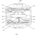
- Fig. 8 shows a PTC thermistor device according to a third embodiment of the present invention.
- the electronic device 100" includes a first support 7" with a first contact part 71" contacting and electrically connecting with the first electrode 51"; a second support 8" with a second contact part 81" contacting and electrically connecting with the second electrode 52"; and a fifth support 10" with a fifth contact part 82" contacting and electrically connecting with the second electrode 52" at a position different from the second contact part 81".
- the first support 7" is mounted on the first terminal 3" and electrically connected therewith.
- the second support 8" and the fifth support 10" are mounted on the second terminal 4" and electrically connected therewith.
- the second support 8" may be integral with the fifth support 10".
- the second support 8" and the fifth support 10" may be integral with the second terminal 4".
- the first support 7" may be integral with the first terminal 3".
- the first support 7" is a rigid support.
- the second support 8" and the fifth support 10" are elastic support.
- the electronic device 100" further comprises a third elastic support 6".
- the third elastic support 6" is such as a spring.
- the third elastic support has a third contact part 63" contacting the first electrode 51" at a position near to the first contact part 71".
- the third contact part 63" is spaced from the first contact part 71 ".
- the third contact part 63" may be contact or overlap with the first contact part 71".
- the third elastic support 6" may include two or other numbers of forks.
- the first contact part 71" is positioned between the two elastic forks and spaced therefrom.
- the spaced distance between the first contact part 71" and the two forks is less than 2mm.
- the first contact part 71" is closer to the center of the electronic element 5" than the second contact part 81" and the fifth contact part 82", and the second contact part 81" and the fifth contact part 82" are opposite to each other across the first contact part 71".
- said first contact part 71" is positioned on the center of the electronic element 5' while a line connecting the second contact part 81" and the fifth contact part 82" passes the center of the electronic element 5".
- the elastic second support 8" applies a second elastic force on the electronic element.
- the elastic fifth support 10" applies a forth elastic force on the electronic element.
- the third elastic support 6 applieslies a first elastic force on the electronic element. The sum of the second elastic force and the fifth elastic force is greater than the first elastic force.
- the first elastic force drives the fragments of the electronic element away from the first support 7", causing the first support 7" out of contact with the first electrode 51", as shown in Fig. 9 . Since the first support 7" is a rigid support without any compression, when the third elastic support 6"pushes away the fragments, the first support 7" does not contact with the electronic element 5" anymore.
- the third elastic support 6" is insulated with the first support 7" and the first terminal 3".
- the third elastic support 6" may be made of an insulated material.
- the third elastic support 6" may be spaced from the first support 7" and the first terminal 3 " or are spaced via insulated material.
- the electrical connection between the electronic element 5" and the first terminal 3" is cut, the fragments are disconnected from the circuit and the short cut is prevented.
Landscapes
- Engineering & Computer Science (AREA)
- Microelectronics & Electronic Packaging (AREA)
- Ceramic Engineering (AREA)
- Physics & Mathematics (AREA)
- Electromagnetism (AREA)
- Thermistors And Varistors (AREA)
Claims (15)
- Elektronische Einrichtung (100), die Folgendes aufweist:ein elektronisches Bauelement (5) mit einer ersten Elektrode (51) und einer zweiten Elektrode (52), die auf dessen entgegengesetzten Seiten angeordnet sind,einen ersten Anschluss (3) und einen zweiten Anschluss (4),eine erste Stütze (7), die am ersten Anschluss (3) angebracht und elektrisch mit diesem verbunden ist, wobei die erste Stütze (7) ein erstes Kontaktteil (71) umfasst, das die erste Elektrode (51) kontaktiert und elektrisch mit dieser verbunden ist,eine zweite Stütze (8), die am zweiten Anschluss (4) angebracht und elektrisch mit diesem verbunden ist, wobei die zweite Stütze (8) ein zweites Kontaktteil (81) umfasst, das die zweite Elektrode (52) kontaktiert und elektrisch mit dieser verbunden ist, undeine dritte elastische Stütze (6), die ein drittes Kontaktteil (63) umfasst, das entweder die erste Elektrode (51) oder die zweite Elektrode (52) kontaktiert,dadurch gekennzeichnet, dass die dritte elastische Stütze (6) dafür vorgesehen ist, ein erstes und ein getrenntes zweites Bruchstück des elektronischen Bauelements (5) außer Kontakt mit der ersten Stütze (7) oder der zweiten Stütze (8) zu schieben, wenn das elektronische Bauelement (5) in einem Ausfallzustand bricht.
- Elektronische Einrichtung (100) nach Anspruch 1, wobei die dritte elastische Stütze (6) gegenüber der ersten Stütze (7) oder zweiten Stütze (8) sowie dem mit dieser elektrisch verbundenen Anschluss elektrisch isoliert wird, wenn das elektronische Bauelement (5) in einem Ausfallzustand bricht.
- Elektronische Einrichtung (100) nach Anspruch 2, wobei es sich bei der entweder ersten Stütze (7) oder zweiten Stütze (8) um eine starre Stütze handelt.
- Elektronische Einrichtung (100) nach Anspruch 3, wobei es sich bei der zweiten Stütze (8) um eine starre Stütze handelt und das dritte Kontaktteil (63) die zweite Elektrode (52) an einer Position nahe des zweiten Kontaktteils (81) kontaktiert.
- Elektronische Einrichtung (100) nach Anspruch 4, wobei die dritte elastische Stütze (6) ein erstes elastisches Teil (61), welches das dritte Kontaktteil (63) bereitstellt, und ein zweites elastisches Teil (62) umfasst, das ein viertes Kontaktteil (64) aufweist, das die zweite Elektrode (52) an einer anderen Position als das zweite Kontaktteil (81) und das dritte Kontaktteil (63) kontaktiert.
- Elektronische Einrichtung (100) nach Anspruch 5, wobei das erste Kontaktteil (71) näher an einer Mitte des elektronischen Bauelements (5) liegt als das zweite Kontaktteil (81) und das vierte Kontaktteil (64), und das zweite Kontaktteil (81) und das vierte Kontaktteil (64) einander quer über das erste Kontaktteil (71) gegenüberliegen.
- Elektronische Einrichtung (100) nach Anspruch 6, wobei das zweite elastische Teil (62) das elektronische Bauelement (5) mit einer zweiten Federkraft beaufschlagt, das erste elastische Teil (61) das elektronische Bauelement (5) mit einer ersten Federkraft beaufschlagt und die zweite Federkraft größer ist als die erste Federkraft.
- Elektronische Einrichtung (100) nach Anspruch 7, wobei Bruchstücke des elektronischen Bauelements (5) durch die erste Federkraft von der zweiten Stütze (8) weggeschoben werden, wenn das elektronische Bauelement (5) in einem Ausfallzustand bricht, so dass die zweite Stütze (8) außer Kontakt mit der zweiten Elektrode (52) ist.
- Elektronische Einrichtung (100) nach Anspruch 7, wobei im Normalzustand aufgrund der ersten Federkraft und der zweiten Federkraft die erste Stütze (7) eine Kraft in Richtung der ersten Elektrode (51) und die zweite Stütze (52) eine Kraft in Richtung der zweiten Elektrode (52) ausübt, so dass die erste Stütze (7) engen Kontakt mit der ersten Elektrode (51) und die zweite Stütze (8) engen Kontakt mit der zweiten Elektrode (52) hält.
- Elektronische Einrichtung (100) nach Anspruch 5, wobei das erste elastische Teil (61) zwei elastische Gabeln (61a, 61b) umfasst und das zweite Kontaktteil (81) zwischen den zwei Gabeln (61a, 61b) positioniert und zu diesen beabstandet ist.
- Elektronische Einrichtung (100) nach Anspruch 10, wobei eine durch das zweite elastische Teil (62) auf das elektronische Bauelement (5) ausgeübte Federkraft größer ist als die Summe der durch die zwei Gabeln (61a, 61b) auf das elektronische Bauelement (5) ausgeübte Federkraft.
- Elektronische Einrichtung (100) nach Anspruch 1, wobei es sich bei dem elektronischen Bauelement (5) um eine Scheibe mit positivem Temperaturkoeffizienten (PTC) handelt.
- Elektronische Einrichtung (100) nach Anspruch 1, wobei die erste Stütze (7) mit dem ersten Anschluss (3) integral ausgebildet ist.
- Elektronische Einrichtung (100) nach Anspruch 1, wobei die zweite Stütze (8) mit dem zweiten Anschluss (4) integral ausgebildet ist.
- Verfahren zum Fertigen einer elektronischen Einrichtung (100), wobei das Verfahren Folgendes umfasst:Auswählen einer elektronischen Einrichtung, die ein elektronisches Bauelement (5) mit einer ersten Elektrode (51) und einer zweiten Elektrode (52), die auf dessen entgegengesetzten Seiten angeordnet sind, einen ersten Anschluss (3) und einen zweiten Anschluss (4), eine erste Stütze (7), die am ersten Anschluss (3) angebracht und elektrisch mit diesem verbunden ist, wobei die erste Stütze (7) ein erstes Kontaktteil (71) umfasst, das die erste Elektrode (51) kontaktiert und elektrisch mit dieser verbunden ist, eine zweite Stütze (8), die am zweiten Anschluss (52) angebracht und elektrisch mit diesem verbunden ist, wobei die zweite Stütze (8) ein zweites Kontaktteil (81) umfasst, das die zweite Elektrode (52) kontaktiert und elektrisch mit dieser verbunden ist, und eine dritte elastische Stütze (6) umfasst, die ein drittes Kontaktteil (63) umfasst, das die erste Elektrode (51) oder die zweite Elektrode (52) kontaktiert, undAnordnen der elektronischen Einrichtung innerhalb einer Abdeckung (1) und eines Sockels (2),dadurch gekennzeichnet, dass die dritte elastische Stütze (6) dafür vorgesehen ist, ein erstes und ein getrenntes zweites Bruchstück des elektronischen Bauelements (5) außer Kontakt mit entweder der ersten Stütze (7) oder der zweiten Stütze (8) zu schieben, wenn das elektronische Bauelement (5) in einem Ausfallzustand bricht.
Applications Claiming Priority (2)
| Application Number | Priority Date | Filing Date | Title |
|---|---|---|---|
| CN201210195769.4A CN103489551B (zh) | 2012-06-14 | 2012-06-14 | 电子器件 |
| CN2012202810688U CN202615954U (zh) | 2012-06-14 | 2012-06-14 | 电子器件 |
Publications (2)
| Publication Number | Publication Date |
|---|---|
| EP2674949A1 EP2674949A1 (de) | 2013-12-18 |
| EP2674949B1 true EP2674949B1 (de) | 2018-08-29 |
Family
ID=49553544
Family Applications (1)
| Application Number | Title | Priority Date | Filing Date |
|---|---|---|---|
| EP13172159.9A Not-in-force EP2674949B1 (de) | 2012-06-14 | 2013-06-14 | PTC-Vorrichtung mit Gehäuse mit elektrischen Abschaltmitteln im Fehlerfall |
Country Status (3)
| Country | Link |
|---|---|
| EP (1) | EP2674949B1 (de) |
| JP (1) | JP6366906B2 (de) |
| KR (1) | KR101887708B1 (de) |
Families Citing this family (2)
| Publication number | Priority date | Publication date | Assignee | Title |
|---|---|---|---|---|
| US10984927B2 (en) | 2019-05-03 | 2021-04-20 | Electrica S.R.L. | PTC thermistor switch for electric motors |
| CN113691166B (zh) * | 2021-08-06 | 2023-06-13 | 杭州星帅尔电器股份有限公司 | 一种ptc起动器 |
Family Cites Families (10)
| Publication number | Priority date | Publication date | Assignee | Title |
|---|---|---|---|---|
| JPS5344017Y2 (de) * | 1974-10-29 | 1978-10-23 | ||
| JPS5521287Y2 (de) * | 1974-12-25 | 1980-05-22 | ||
| JPS51116966A (en) * | 1975-04-04 | 1976-10-14 | Tasuku Okazaki | Overrheating protector |
| JPH07335408A (ja) * | 1994-06-10 | 1995-12-22 | Murata Mfg Co Ltd | 発熱電子部品 |
| JP2891179B2 (ja) * | 1996-05-10 | 1999-05-17 | 株式会社村田製作所 | 電子部品 |
| DE19638631C2 (de) * | 1996-09-20 | 2002-09-26 | Epcos Ag | Kontaktgruppe für Halbleiter-Widerstände, wie Kaltleiter |
| DE19824781B4 (de) * | 1998-06-03 | 2005-05-19 | Epcos Ag | Elektrisches Bauelement, insbesondere Schaltkaltleiter |
| JP3567854B2 (ja) * | 2000-05-18 | 2004-09-22 | 株式会社村田製作所 | 電子部品 |
| JP3811804B2 (ja) * | 2003-08-26 | 2006-08-23 | 株式会社センサータ・テクノロジーズジャパン | モータ始動用リレーおよびそれを用いた電動圧縮機 |
| US8174354B2 (en) * | 2010-07-23 | 2012-05-08 | Sensata Technologies Massachusetts, Inc. | Method and apparatus for control of failed thermistor devices |
-
2013
- 2013-06-14 JP JP2013125182A patent/JP6366906B2/ja not_active Expired - Fee Related
- 2013-06-14 KR KR1020130068254A patent/KR101887708B1/ko not_active Expired - Fee Related
- 2013-06-14 EP EP13172159.9A patent/EP2674949B1/de not_active Not-in-force
Also Published As
| Publication number | Publication date |
|---|---|
| KR20130140585A (ko) | 2013-12-24 |
| JP2014003295A (ja) | 2014-01-09 |
| KR101887708B1 (ko) | 2018-08-10 |
| JP6366906B2 (ja) | 2018-08-01 |
| EP2674949A1 (de) | 2013-12-18 |
Similar Documents
| Publication | Publication Date | Title |
|---|---|---|
| US9496112B2 (en) | Electric device | |
| JP3567854B2 (ja) | 電子部品 | |
| US6686722B2 (en) | Battery pack containing a circuit breaker | |
| US20100219929A1 (en) | Thermal fuse with current fuse function | |
| US9431821B2 (en) | Electronic device | |
| KR101796787B1 (ko) | 오작동 서미스터 디바이스의 제어를 위한 방법 및 장치 | |
| US20140300443A1 (en) | Thermal protector | |
| EP2674949B1 (de) | PTC-Vorrichtung mit Gehäuse mit elektrischen Abschaltmitteln im Fehlerfall | |
| KR101914186B1 (ko) | 접점 구조 | |
| US9472363B2 (en) | Thermal protector | |
| CN103489551B (zh) | 电子器件 | |
| JP2882322B2 (ja) | 電子部品 | |
| US10056211B2 (en) | Heat-reactive switch | |
| EP2159812A1 (de) | Überstromschutzvorrichtung | |
| CN102158148A (zh) | 起动装置 | |
| JP2003332104A (ja) | モータの起動装置 | |
| CN221446898U (zh) | 热敏电阻起动器 | |
| JP2897699B2 (ja) | 電子部品 | |
| JP5578716B2 (ja) | 温度ヒューズ | |
| KR100982041B1 (ko) | 온도조절장치 | |
| JPH06251852A (ja) | 避雷管 | |
| KR20080097755A (ko) | 무접점 기동장치 |
Legal Events
| Date | Code | Title | Description |
|---|---|---|---|
| PUAI | Public reference made under article 153(3) epc to a published international application that has entered the european phase |
Free format text: ORIGINAL CODE: 0009012 |
|
| AK | Designated contracting states |
Kind code of ref document: A1 Designated state(s): AL AT BE BG CH CY CZ DE DK EE ES FI FR GB GR HR HU IE IS IT LI LT LU LV MC MK MT NL NO PL PT RO RS SE SI SK SM TR |
|
| AX | Request for extension of the european patent |
Extension state: BA ME |
|
| 17P | Request for examination filed |
Effective date: 20140617 |
|
| RBV | Designated contracting states (corrected) |
Designated state(s): AL AT BE BG CH CY CZ DE DK EE ES FI FR GB GR HR HU IE IS IT LI LT LU LV MC MK MT NL NO PL PT RO RS SE SI SK SM TR |
|
| RAP1 | Party data changed (applicant data changed or rights of an application transferred) |
Owner name: SENSATA TECHNOLOGIES, INC. |
|
| STAA | Information on the status of an ep patent application or granted ep patent |
Free format text: STATUS: EXAMINATION IS IN PROGRESS |
|
| 17Q | First examination report despatched |
Effective date: 20170908 |
|
| GRAP | Despatch of communication of intention to grant a patent |
Free format text: ORIGINAL CODE: EPIDOSNIGR1 |
|
| STAA | Information on the status of an ep patent application or granted ep patent |
Free format text: STATUS: GRANT OF PATENT IS INTENDED |
|
| INTG | Intention to grant announced |
Effective date: 20180307 |
|
| GRAJ | Information related to disapproval of communication of intention to grant by the applicant or resumption of examination proceedings by the epo deleted |
Free format text: ORIGINAL CODE: EPIDOSDIGR1 |
|
| STAA | Information on the status of an ep patent application or granted ep patent |
Free format text: STATUS: EXAMINATION IS IN PROGRESS |
|
| GRAR | Information related to intention to grant a patent recorded |
Free format text: ORIGINAL CODE: EPIDOSNIGR71 |
|
| GRAS | Grant fee paid |
Free format text: ORIGINAL CODE: EPIDOSNIGR3 |
|
| STAA | Information on the status of an ep patent application or granted ep patent |
Free format text: STATUS: GRANT OF PATENT IS INTENDED |
|
| GRAA | (expected) grant |
Free format text: ORIGINAL CODE: 0009210 |
|
| STAA | Information on the status of an ep patent application or granted ep patent |
Free format text: STATUS: THE PATENT HAS BEEN GRANTED |
|
| INTC | Intention to grant announced (deleted) | ||
| AK | Designated contracting states |
Kind code of ref document: B1 Designated state(s): AL AT BE BG CH CY CZ DE DK EE ES FI FR GB GR HR HU IE IS IT LI LT LU LV MC MK MT NL NO PL PT RO RS SE SI SK SM TR |
|
| INTG | Intention to grant announced |
Effective date: 20180724 |
|
| REG | Reference to a national code |
Ref country code: GB Ref legal event code: FG4D |
|
| REG | Reference to a national code |
Ref country code: CH Ref legal event code: EP |
|
| REG | Reference to a national code |
Ref country code: AT Ref legal event code: REF Ref document number: 1036119 Country of ref document: AT Kind code of ref document: T Effective date: 20180915 |
|
| REG | Reference to a national code |
Ref country code: IE Ref legal event code: FG4D |
|
| REG | Reference to a national code |
Ref country code: DE Ref legal event code: R096 Ref document number: 602013042656 Country of ref document: DE |
|
| REG | Reference to a national code |
Ref country code: NL Ref legal event code: MP Effective date: 20180829 |
|
| REG | Reference to a national code |
Ref country code: LT Ref legal event code: MG4D |
|
| PG25 | Lapsed in a contracting state [announced via postgrant information from national office to epo] |
Ref country code: SE Free format text: LAPSE BECAUSE OF FAILURE TO SUBMIT A TRANSLATION OF THE DESCRIPTION OR TO PAY THE FEE WITHIN THE PRESCRIBED TIME-LIMIT Effective date: 20180829 Ref country code: BG Free format text: LAPSE BECAUSE OF FAILURE TO SUBMIT A TRANSLATION OF THE DESCRIPTION OR TO PAY THE FEE WITHIN THE PRESCRIBED TIME-LIMIT Effective date: 20181129 Ref country code: NL Free format text: LAPSE BECAUSE OF FAILURE TO SUBMIT A TRANSLATION OF THE DESCRIPTION OR TO PAY THE FEE WITHIN THE PRESCRIBED TIME-LIMIT Effective date: 20180829 Ref country code: LT Free format text: LAPSE BECAUSE OF FAILURE TO SUBMIT A TRANSLATION OF THE DESCRIPTION OR TO PAY THE FEE WITHIN THE PRESCRIBED TIME-LIMIT Effective date: 20180829 Ref country code: GR Free format text: LAPSE BECAUSE OF FAILURE TO SUBMIT A TRANSLATION OF THE DESCRIPTION OR TO PAY THE FEE WITHIN THE PRESCRIBED TIME-LIMIT Effective date: 20181130 Ref country code: FI Free format text: LAPSE BECAUSE OF FAILURE TO SUBMIT A TRANSLATION OF THE DESCRIPTION OR TO PAY THE FEE WITHIN THE PRESCRIBED TIME-LIMIT Effective date: 20180829 Ref country code: NO Free format text: LAPSE BECAUSE OF FAILURE TO SUBMIT A TRANSLATION OF THE DESCRIPTION OR TO PAY THE FEE WITHIN THE PRESCRIBED TIME-LIMIT Effective date: 20181129 Ref country code: IS Free format text: LAPSE BECAUSE OF FAILURE TO SUBMIT A TRANSLATION OF THE DESCRIPTION OR TO PAY THE FEE WITHIN THE PRESCRIBED TIME-LIMIT Effective date: 20181229 Ref country code: RS Free format text: LAPSE BECAUSE OF FAILURE TO SUBMIT A TRANSLATION OF THE DESCRIPTION OR TO PAY THE FEE WITHIN THE PRESCRIBED TIME-LIMIT Effective date: 20180829 |
|
| REG | Reference to a national code |
Ref country code: AT Ref legal event code: MK05 Ref document number: 1036119 Country of ref document: AT Kind code of ref document: T Effective date: 20180829 |
|
| PG25 | Lapsed in a contracting state [announced via postgrant information from national office to epo] |
Ref country code: HR Free format text: LAPSE BECAUSE OF FAILURE TO SUBMIT A TRANSLATION OF THE DESCRIPTION OR TO PAY THE FEE WITHIN THE PRESCRIBED TIME-LIMIT Effective date: 20180829 Ref country code: LV Free format text: LAPSE BECAUSE OF FAILURE TO SUBMIT A TRANSLATION OF THE DESCRIPTION OR TO PAY THE FEE WITHIN THE PRESCRIBED TIME-LIMIT Effective date: 20180829 Ref country code: AL Free format text: LAPSE BECAUSE OF FAILURE TO SUBMIT A TRANSLATION OF THE DESCRIPTION OR TO PAY THE FEE WITHIN THE PRESCRIBED TIME-LIMIT Effective date: 20180829 |
|
| PG25 | Lapsed in a contracting state [announced via postgrant information from national office to epo] |
Ref country code: EE Free format text: LAPSE BECAUSE OF FAILURE TO SUBMIT A TRANSLATION OF THE DESCRIPTION OR TO PAY THE FEE WITHIN THE PRESCRIBED TIME-LIMIT Effective date: 20180829 Ref country code: AT Free format text: LAPSE BECAUSE OF FAILURE TO SUBMIT A TRANSLATION OF THE DESCRIPTION OR TO PAY THE FEE WITHIN THE PRESCRIBED TIME-LIMIT Effective date: 20180829 Ref country code: IT Free format text: LAPSE BECAUSE OF FAILURE TO SUBMIT A TRANSLATION OF THE DESCRIPTION OR TO PAY THE FEE WITHIN THE PRESCRIBED TIME-LIMIT Effective date: 20180829 Ref country code: CZ Free format text: LAPSE BECAUSE OF FAILURE TO SUBMIT A TRANSLATION OF THE DESCRIPTION OR TO PAY THE FEE WITHIN THE PRESCRIBED TIME-LIMIT Effective date: 20180829 Ref country code: RO Free format text: LAPSE BECAUSE OF FAILURE TO SUBMIT A TRANSLATION OF THE DESCRIPTION OR TO PAY THE FEE WITHIN THE PRESCRIBED TIME-LIMIT Effective date: 20180829 Ref country code: ES Free format text: LAPSE BECAUSE OF FAILURE TO SUBMIT A TRANSLATION OF THE DESCRIPTION OR TO PAY THE FEE WITHIN THE PRESCRIBED TIME-LIMIT Effective date: 20180829 Ref country code: PL Free format text: LAPSE BECAUSE OF FAILURE TO SUBMIT A TRANSLATION OF THE DESCRIPTION OR TO PAY THE FEE WITHIN THE PRESCRIBED TIME-LIMIT Effective date: 20180829 |
|
| PG25 | Lapsed in a contracting state [announced via postgrant information from national office to epo] |
Ref country code: SK Free format text: LAPSE BECAUSE OF FAILURE TO SUBMIT A TRANSLATION OF THE DESCRIPTION OR TO PAY THE FEE WITHIN THE PRESCRIBED TIME-LIMIT Effective date: 20180829 Ref country code: SM Free format text: LAPSE BECAUSE OF FAILURE TO SUBMIT A TRANSLATION OF THE DESCRIPTION OR TO PAY THE FEE WITHIN THE PRESCRIBED TIME-LIMIT Effective date: 20180829 Ref country code: DK Free format text: LAPSE BECAUSE OF FAILURE TO SUBMIT A TRANSLATION OF THE DESCRIPTION OR TO PAY THE FEE WITHIN THE PRESCRIBED TIME-LIMIT Effective date: 20180829 |
|
| REG | Reference to a national code |
Ref country code: DE Ref legal event code: R097 Ref document number: 602013042656 Country of ref document: DE |
|
| PLBE | No opposition filed within time limit |
Free format text: ORIGINAL CODE: 0009261 |
|
| STAA | Information on the status of an ep patent application or granted ep patent |
Free format text: STATUS: NO OPPOSITION FILED WITHIN TIME LIMIT |
|
| 26N | No opposition filed |
Effective date: 20190531 |
|
| PG25 | Lapsed in a contracting state [announced via postgrant information from national office to epo] |
Ref country code: SI Free format text: LAPSE BECAUSE OF FAILURE TO SUBMIT A TRANSLATION OF THE DESCRIPTION OR TO PAY THE FEE WITHIN THE PRESCRIBED TIME-LIMIT Effective date: 20180829 |
|
| PG25 | Lapsed in a contracting state [announced via postgrant information from national office to epo] |
Ref country code: MC Free format text: LAPSE BECAUSE OF FAILURE TO SUBMIT A TRANSLATION OF THE DESCRIPTION OR TO PAY THE FEE WITHIN THE PRESCRIBED TIME-LIMIT Effective date: 20180829 |
|
| REG | Reference to a national code |
Ref country code: CH Ref legal event code: PL |
|
| REG | Reference to a national code |
Ref country code: BE Ref legal event code: MM Effective date: 20190630 |
|
| PG25 | Lapsed in a contracting state [announced via postgrant information from national office to epo] |
Ref country code: TR Free format text: LAPSE BECAUSE OF FAILURE TO SUBMIT A TRANSLATION OF THE DESCRIPTION OR TO PAY THE FEE WITHIN THE PRESCRIBED TIME-LIMIT Effective date: 20180829 |
|
| PG25 | Lapsed in a contracting state [announced via postgrant information from national office to epo] |
Ref country code: IE Free format text: LAPSE BECAUSE OF NON-PAYMENT OF DUE FEES Effective date: 20190614 |
|
| PG25 | Lapsed in a contracting state [announced via postgrant information from national office to epo] |
Ref country code: LI Free format text: LAPSE BECAUSE OF NON-PAYMENT OF DUE FEES Effective date: 20190630 Ref country code: CH Free format text: LAPSE BECAUSE OF NON-PAYMENT OF DUE FEES Effective date: 20190630 Ref country code: LU Free format text: LAPSE BECAUSE OF NON-PAYMENT OF DUE FEES Effective date: 20190614 Ref country code: BE Free format text: LAPSE BECAUSE OF NON-PAYMENT OF DUE FEES Effective date: 20190630 |
|
| PG25 | Lapsed in a contracting state [announced via postgrant information from national office to epo] |
Ref country code: FR Free format text: LAPSE BECAUSE OF NON-PAYMENT OF DUE FEES Effective date: 20190630 Ref country code: PT Free format text: LAPSE BECAUSE OF FAILURE TO SUBMIT A TRANSLATION OF THE DESCRIPTION OR TO PAY THE FEE WITHIN THE PRESCRIBED TIME-LIMIT Effective date: 20181229 |
|
| PG25 | Lapsed in a contracting state [announced via postgrant information from national office to epo] |
Ref country code: CY Free format text: LAPSE BECAUSE OF FAILURE TO SUBMIT A TRANSLATION OF THE DESCRIPTION OR TO PAY THE FEE WITHIN THE PRESCRIBED TIME-LIMIT Effective date: 20180829 |
|
| PG25 | Lapsed in a contracting state [announced via postgrant information from national office to epo] |
Ref country code: MT Free format text: LAPSE BECAUSE OF FAILURE TO SUBMIT A TRANSLATION OF THE DESCRIPTION OR TO PAY THE FEE WITHIN THE PRESCRIBED TIME-LIMIT Effective date: 20180829 Ref country code: HU Free format text: LAPSE BECAUSE OF FAILURE TO SUBMIT A TRANSLATION OF THE DESCRIPTION OR TO PAY THE FEE WITHIN THE PRESCRIBED TIME-LIMIT; INVALID AB INITIO Effective date: 20130614 |
|
| PG25 | Lapsed in a contracting state [announced via postgrant information from national office to epo] |
Ref country code: MK Free format text: LAPSE BECAUSE OF FAILURE TO SUBMIT A TRANSLATION OF THE DESCRIPTION OR TO PAY THE FEE WITHIN THE PRESCRIBED TIME-LIMIT Effective date: 20180829 |
|
| PGFP | Annual fee paid to national office [announced via postgrant information from national office to epo] |
Ref country code: GB Payment date: 20220628 Year of fee payment: 10 |
|
| PGFP | Annual fee paid to national office [announced via postgrant information from national office to epo] |
Ref country code: DE Payment date: 20220629 Year of fee payment: 10 |
|
| P01 | Opt-out of the competence of the unified patent court (upc) registered |
Effective date: 20230529 |
|
| REG | Reference to a national code |
Ref country code: DE Ref legal event code: R119 Ref document number: 602013042656 Country of ref document: DE |
|
| GBPC | Gb: european patent ceased through non-payment of renewal fee |
Effective date: 20230614 |
|
| PG25 | Lapsed in a contracting state [announced via postgrant information from national office to epo] |
Ref country code: DE Free format text: LAPSE BECAUSE OF NON-PAYMENT OF DUE FEES Effective date: 20240103 Ref country code: GB Free format text: LAPSE BECAUSE OF NON-PAYMENT OF DUE FEES Effective date: 20230614 |