EP2677541A1 - Verfahren zum Drahtbonden eines Leistungshalbleiterbausteins sowie die enstprechende Vorrichtung - Google Patents
Verfahren zum Drahtbonden eines Leistungshalbleiterbausteins sowie die enstprechende Vorrichtung Download PDFInfo
- Publication number
- EP2677541A1 EP2677541A1 EP12172513.9A EP12172513A EP2677541A1 EP 2677541 A1 EP2677541 A1 EP 2677541A1 EP 12172513 A EP12172513 A EP 12172513A EP 2677541 A1 EP2677541 A1 EP 2677541A1
- Authority
- EP
- European Patent Office
- Prior art keywords
- bonding
- contact pad
- substrate
- bonding means
- metallization
- Prior art date
- Legal status (The legal status is an assumption and is not a legal conclusion. Google has not performed a legal analysis and makes no representation as to the accuracy of the status listed.)
- Withdrawn
Links
Images

Classifications
-
- H—ELECTRICITY
- H10—SEMICONDUCTOR DEVICES; ELECTRIC SOLID-STATE DEVICES NOT OTHERWISE PROVIDED FOR
- H10W—GENERIC PACKAGES, INTERCONNECTIONS, CONNECTORS OR OTHER CONSTRUCTIONAL DETAILS OF DEVICES COVERED BY CLASS H10
- H10W90/00—Package configurations
-
- H—ELECTRICITY
- H10—SEMICONDUCTOR DEVICES; ELECTRIC SOLID-STATE DEVICES NOT OTHERWISE PROVIDED FOR
- H10W—GENERIC PACKAGES, INTERCONNECTIONS, CONNECTORS OR OTHER CONSTRUCTIONAL DETAILS OF DEVICES COVERED BY CLASS H10
- H10W72/00—Interconnections or connectors in packages
- H10W72/01—Manufacture or treatment
- H10W72/015—Manufacture or treatment of bond wires
- H10W72/01515—Forming coatings
-
- H—ELECTRICITY
- H10—SEMICONDUCTOR DEVICES; ELECTRIC SOLID-STATE DEVICES NOT OTHERWISE PROVIDED FOR
- H10W—GENERIC PACKAGES, INTERCONNECTIONS, CONNECTORS OR OTHER CONSTRUCTIONAL DETAILS OF DEVICES COVERED BY CLASS H10
- H10W72/00—Interconnections or connectors in packages
- H10W72/071—Connecting or disconnecting
- H10W72/073—Connecting or disconnecting of die-attach connectors
-
- H—ELECTRICITY
- H10—SEMICONDUCTOR DEVICES; ELECTRIC SOLID-STATE DEVICES NOT OTHERWISE PROVIDED FOR
- H10W—GENERIC PACKAGES, INTERCONNECTIONS, CONNECTORS OR OTHER CONSTRUCTIONAL DETAILS OF DEVICES COVERED BY CLASS H10
- H10W72/00—Interconnections or connectors in packages
- H10W72/071—Connecting or disconnecting
- H10W72/073—Connecting or disconnecting of die-attach connectors
- H10W72/07331—Connecting techniques
-
- H—ELECTRICITY
- H10—SEMICONDUCTOR DEVICES; ELECTRIC SOLID-STATE DEVICES NOT OTHERWISE PROVIDED FOR
- H10W—GENERIC PACKAGES, INTERCONNECTIONS, CONNECTORS OR OTHER CONSTRUCTIONAL DETAILS OF DEVICES COVERED BY CLASS H10
- H10W72/00—Interconnections or connectors in packages
- H10W72/071—Connecting or disconnecting
- H10W72/073—Connecting or disconnecting of die-attach connectors
- H10W72/07331—Connecting techniques
- H10W72/07336—Soldering or alloying
-
- H—ELECTRICITY
- H10—SEMICONDUCTOR DEVICES; ELECTRIC SOLID-STATE DEVICES NOT OTHERWISE PROVIDED FOR
- H10W—GENERIC PACKAGES, INTERCONNECTIONS, CONNECTORS OR OTHER CONSTRUCTIONAL DETAILS OF DEVICES COVERED BY CLASS H10
- H10W72/00—Interconnections or connectors in packages
- H10W72/071—Connecting or disconnecting
- H10W72/075—Connecting or disconnecting of bond wires
-
- H—ELECTRICITY
- H10—SEMICONDUCTOR DEVICES; ELECTRIC SOLID-STATE DEVICES NOT OTHERWISE PROVIDED FOR
- H10W—GENERIC PACKAGES, INTERCONNECTIONS, CONNECTORS OR OTHER CONSTRUCTIONAL DETAILS OF DEVICES COVERED BY CLASS H10
- H10W72/00—Interconnections or connectors in packages
- H10W72/071—Connecting or disconnecting
- H10W72/075—Connecting or disconnecting of bond wires
- H10W72/07551—Connecting or disconnecting of bond wires characterised by changes in properties of the bond wires during the connecting
- H10W72/07553—Connecting or disconnecting of bond wires characterised by changes in properties of the bond wires during the connecting changes in shapes
-
- H—ELECTRICITY
- H10—SEMICONDUCTOR DEVICES; ELECTRIC SOLID-STATE DEVICES NOT OTHERWISE PROVIDED FOR
- H10W—GENERIC PACKAGES, INTERCONNECTIONS, CONNECTORS OR OTHER CONSTRUCTIONAL DETAILS OF DEVICES COVERED BY CLASS H10
- H10W72/00—Interconnections or connectors in packages
- H10W72/071—Connecting or disconnecting
- H10W72/075—Connecting or disconnecting of bond wires
- H10W72/07551—Connecting or disconnecting of bond wires characterised by changes in properties of the bond wires during the connecting
- H10W72/07554—Connecting or disconnecting of bond wires characterised by changes in properties of the bond wires during the connecting changes in dispositions
-
- H—ELECTRICITY
- H10—SEMICONDUCTOR DEVICES; ELECTRIC SOLID-STATE DEVICES NOT OTHERWISE PROVIDED FOR
- H10W—GENERIC PACKAGES, INTERCONNECTIONS, CONNECTORS OR OTHER CONSTRUCTIONAL DETAILS OF DEVICES COVERED BY CLASS H10
- H10W72/00—Interconnections or connectors in packages
- H10W72/071—Connecting or disconnecting
- H10W72/075—Connecting or disconnecting of bond wires
- H10W72/07551—Connecting or disconnecting of bond wires characterised by changes in properties of the bond wires during the connecting
- H10W72/07555—Connecting or disconnecting of bond wires characterised by changes in properties of the bond wires during the connecting changes in materials
-
- H—ELECTRICITY
- H10—SEMICONDUCTOR DEVICES; ELECTRIC SOLID-STATE DEVICES NOT OTHERWISE PROVIDED FOR
- H10W—GENERIC PACKAGES, INTERCONNECTIONS, CONNECTORS OR OTHER CONSTRUCTIONAL DETAILS OF DEVICES COVERED BY CLASS H10
- H10W72/00—Interconnections or connectors in packages
- H10W72/50—Bond wires
- H10W72/531—Shapes of wire connectors
- H10W72/533—Cross-sectional shape
- H10W72/534—Cross-sectional shape being rectangular
-
- H—ELECTRICITY
- H10—SEMICONDUCTOR DEVICES; ELECTRIC SOLID-STATE DEVICES NOT OTHERWISE PROVIDED FOR
- H10W—GENERIC PACKAGES, INTERCONNECTIONS, CONNECTORS OR OTHER CONSTRUCTIONAL DETAILS OF DEVICES COVERED BY CLASS H10
- H10W72/00—Interconnections or connectors in packages
- H10W72/50—Bond wires
- H10W72/531—Shapes of wire connectors
- H10W72/5363—Shapes of wire connectors the connected ends being wedge-shaped
-
- H—ELECTRICITY
- H10—SEMICONDUCTOR DEVICES; ELECTRIC SOLID-STATE DEVICES NOT OTHERWISE PROVIDED FOR
- H10W—GENERIC PACKAGES, INTERCONNECTIONS, CONNECTORS OR OTHER CONSTRUCTIONAL DETAILS OF DEVICES COVERED BY CLASS H10
- H10W72/00—Interconnections or connectors in packages
- H10W72/50—Bond wires
- H10W72/531—Shapes of wire connectors
- H10W72/5366—Shapes of wire connectors the bond wires having kinks
-
- H—ELECTRICITY
- H10—SEMICONDUCTOR DEVICES; ELECTRIC SOLID-STATE DEVICES NOT OTHERWISE PROVIDED FOR
- H10W—GENERIC PACKAGES, INTERCONNECTIONS, CONNECTORS OR OTHER CONSTRUCTIONAL DETAILS OF DEVICES COVERED BY CLASS H10
- H10W72/00—Interconnections or connectors in packages
- H10W72/50—Bond wires
- H10W72/541—Dispositions of bond wires
- H10W72/547—Dispositions of multiple bond wires
-
- H—ELECTRICITY
- H10—SEMICONDUCTOR DEVICES; ELECTRIC SOLID-STATE DEVICES NOT OTHERWISE PROVIDED FOR
- H10W—GENERIC PACKAGES, INTERCONNECTIONS, CONNECTORS OR OTHER CONSTRUCTIONAL DETAILS OF DEVICES COVERED BY CLASS H10
- H10W72/00—Interconnections or connectors in packages
- H10W72/50—Bond wires
- H10W72/541—Dispositions of bond wires
- H10W72/547—Dispositions of multiple bond wires
- H10W72/5473—Dispositions of multiple bond wires multiple bond wires connected to a common bond pad
-
- H—ELECTRICITY
- H10—SEMICONDUCTOR DEVICES; ELECTRIC SOLID-STATE DEVICES NOT OTHERWISE PROVIDED FOR
- H10W—GENERIC PACKAGES, INTERCONNECTIONS, CONNECTORS OR OTHER CONSTRUCTIONAL DETAILS OF DEVICES COVERED BY CLASS H10
- H10W72/00—Interconnections or connectors in packages
- H10W72/50—Bond wires
- H10W72/541—Dispositions of bond wires
- H10W72/547—Dispositions of multiple bond wires
- H10W72/5475—Dispositions of multiple bond wires multiple bond wires connected to common bond pads at both ends of the wires
-
- H—ELECTRICITY
- H10—SEMICONDUCTOR DEVICES; ELECTRIC SOLID-STATE DEVICES NOT OTHERWISE PROVIDED FOR
- H10W—GENERIC PACKAGES, INTERCONNECTIONS, CONNECTORS OR OTHER CONSTRUCTIONAL DETAILS OF DEVICES COVERED BY CLASS H10
- H10W72/00—Interconnections or connectors in packages
- H10W72/50—Bond wires
- H10W72/551—Materials of bond wires
- H10W72/552—Materials of bond wires comprising metals or metalloids, e.g. silver
-
- H—ELECTRICITY
- H10—SEMICONDUCTOR DEVICES; ELECTRIC SOLID-STATE DEVICES NOT OTHERWISE PROVIDED FOR
- H10W—GENERIC PACKAGES, INTERCONNECTIONS, CONNECTORS OR OTHER CONSTRUCTIONAL DETAILS OF DEVICES COVERED BY CLASS H10
- H10W72/00—Interconnections or connectors in packages
- H10W72/50—Bond wires
- H10W72/551—Materials of bond wires
- H10W72/552—Materials of bond wires comprising metals or metalloids, e.g. silver
- H10W72/5524—Materials of bond wires comprising metals or metalloids, e.g. silver comprising aluminium [Al]
-
- H—ELECTRICITY
- H10—SEMICONDUCTOR DEVICES; ELECTRIC SOLID-STATE DEVICES NOT OTHERWISE PROVIDED FOR
- H10W—GENERIC PACKAGES, INTERCONNECTIONS, CONNECTORS OR OTHER CONSTRUCTIONAL DETAILS OF DEVICES COVERED BY CLASS H10
- H10W72/00—Interconnections or connectors in packages
- H10W72/50—Bond wires
- H10W72/551—Materials of bond wires
- H10W72/552—Materials of bond wires comprising metals or metalloids, e.g. silver
- H10W72/5525—Materials of bond wires comprising metals or metalloids, e.g. silver comprising copper [Cu]
-
- H—ELECTRICITY
- H10—SEMICONDUCTOR DEVICES; ELECTRIC SOLID-STATE DEVICES NOT OTHERWISE PROVIDED FOR
- H10W—GENERIC PACKAGES, INTERCONNECTIONS, CONNECTORS OR OTHER CONSTRUCTIONAL DETAILS OF DEVICES COVERED BY CLASS H10
- H10W72/00—Interconnections or connectors in packages
- H10W72/50—Bond wires
- H10W72/551—Materials of bond wires
- H10W72/555—Materials of bond wires of outermost layers of multilayered bond wires, e.g. material of a coating
-
- H—ELECTRICITY
- H10—SEMICONDUCTOR DEVICES; ELECTRIC SOLID-STATE DEVICES NOT OTHERWISE PROVIDED FOR
- H10W—GENERIC PACKAGES, INTERCONNECTIONS, CONNECTORS OR OTHER CONSTRUCTIONAL DETAILS OF DEVICES COVERED BY CLASS H10
- H10W72/00—Interconnections or connectors in packages
- H10W72/50—Bond wires
- H10W72/551—Materials of bond wires
- H10W72/557—Multiple bond wires having different materials
-
- H—ELECTRICITY
- H10—SEMICONDUCTOR DEVICES; ELECTRIC SOLID-STATE DEVICES NOT OTHERWISE PROVIDED FOR
- H10W—GENERIC PACKAGES, INTERCONNECTIONS, CONNECTORS OR OTHER CONSTRUCTIONAL DETAILS OF DEVICES COVERED BY CLASS H10
- H10W72/00—Interconnections or connectors in packages
- H10W72/50—Bond wires
- H10W72/581—Auxiliary members, e.g. flow barriers
- H10W72/583—Reinforcing structures
-
- H—ELECTRICITY
- H10—SEMICONDUCTOR DEVICES; ELECTRIC SOLID-STATE DEVICES NOT OTHERWISE PROVIDED FOR
- H10W—GENERIC PACKAGES, INTERCONNECTIONS, CONNECTORS OR OTHER CONSTRUCTIONAL DETAILS OF DEVICES COVERED BY CLASS H10
- H10W72/00—Interconnections or connectors in packages
- H10W72/50—Bond wires
- H10W72/59—Bond pads specially adapted therefor
-
- H—ELECTRICITY
- H10—SEMICONDUCTOR DEVICES; ELECTRIC SOLID-STATE DEVICES NOT OTHERWISE PROVIDED FOR
- H10W—GENERIC PACKAGES, INTERCONNECTIONS, CONNECTORS OR OTHER CONSTRUCTIONAL DETAILS OF DEVICES COVERED BY CLASS H10
- H10W72/00—Interconnections or connectors in packages
- H10W72/851—Dispositions of multiple connectors or interconnections
- H10W72/874—On different surfaces
- H10W72/884—Die-attach connectors and bond wires
-
- H—ELECTRICITY
- H10—SEMICONDUCTOR DEVICES; ELECTRIC SOLID-STATE DEVICES NOT OTHERWISE PROVIDED FOR
- H10W—GENERIC PACKAGES, INTERCONNECTIONS, CONNECTORS OR OTHER CONSTRUCTIONAL DETAILS OF DEVICES COVERED BY CLASS H10
- H10W72/00—Interconnections or connectors in packages
- H10W72/90—Bond pads, in general
- H10W72/921—Structures or relative sizes of bond pads
- H10W72/923—Bond pads having multiple stacked layers
-
- H—ELECTRICITY
- H10—SEMICONDUCTOR DEVICES; ELECTRIC SOLID-STATE DEVICES NOT OTHERWISE PROVIDED FOR
- H10W—GENERIC PACKAGES, INTERCONNECTIONS, CONNECTORS OR OTHER CONSTRUCTIONAL DETAILS OF DEVICES COVERED BY CLASS H10
- H10W72/00—Interconnections or connectors in packages
- H10W72/90—Bond pads, in general
- H10W72/921—Structures or relative sizes of bond pads
- H10W72/926—Multiple bond pads having different sizes
-
- H—ELECTRICITY
- H10—SEMICONDUCTOR DEVICES; ELECTRIC SOLID-STATE DEVICES NOT OTHERWISE PROVIDED FOR
- H10W—GENERIC PACKAGES, INTERCONNECTIONS, CONNECTORS OR OTHER CONSTRUCTIONAL DETAILS OF DEVICES COVERED BY CLASS H10
- H10W72/00—Interconnections or connectors in packages
- H10W72/90—Bond pads, in general
- H10W72/931—Shapes of bond pads
- H10W72/932—Plan-view shape, i.e. in top view
-
- H—ELECTRICITY
- H10—SEMICONDUCTOR DEVICES; ELECTRIC SOLID-STATE DEVICES NOT OTHERWISE PROVIDED FOR
- H10W—GENERIC PACKAGES, INTERCONNECTIONS, CONNECTORS OR OTHER CONSTRUCTIONAL DETAILS OF DEVICES COVERED BY CLASS H10
- H10W72/00—Interconnections or connectors in packages
- H10W72/90—Bond pads, in general
- H10W72/951—Materials of bond pads
- H10W72/952—Materials of bond pads comprising metals or metalloids, e.g. PbSn, Ag or Cu
-
- H—ELECTRICITY
- H10—SEMICONDUCTOR DEVICES; ELECTRIC SOLID-STATE DEVICES NOT OTHERWISE PROVIDED FOR
- H10W—GENERIC PACKAGES, INTERCONNECTIONS, CONNECTORS OR OTHER CONSTRUCTIONAL DETAILS OF DEVICES COVERED BY CLASS H10
- H10W90/00—Package configurations
- H10W90/701—Package configurations characterised by the relative positions of pads or connectors relative to package parts
- H10W90/731—Package configurations characterised by the relative positions of pads or connectors relative to package parts of die-attach connectors
- H10W90/734—Package configurations characterised by the relative positions of pads or connectors relative to package parts of die-attach connectors between a chip and a stacked insulating package substrate, interposer or RDL
-
- H—ELECTRICITY
- H10—SEMICONDUCTOR DEVICES; ELECTRIC SOLID-STATE DEVICES NOT OTHERWISE PROVIDED FOR
- H10W—GENERIC PACKAGES, INTERCONNECTIONS, CONNECTORS OR OTHER CONSTRUCTIONAL DETAILS OF DEVICES COVERED BY CLASS H10
- H10W90/00—Package configurations
- H10W90/701—Package configurations characterised by the relative positions of pads or connectors relative to package parts
- H10W90/751—Package configurations characterised by the relative positions of pads or connectors relative to package parts of bond wires
- H10W90/754—Package configurations characterised by the relative positions of pads or connectors relative to package parts of bond wires between a chip and a stacked insulating package substrate, interposer or RDL
Definitions
- the present invention relates to a method for bonding a contact pad of a power semiconductor, which is arranged on a substrate, to a metallization of the substrate.
- the present invention also relates to a substrate with a power semiconductor mounted thereon, whereby the substrate comprises a metallization, the power semiconductor has a contact pad, and at least one bonding means of soft metal is bonded between the contact pad and the metallization.
- the electrical connection of power semiconductors on substrates is an important issue, especially in the area of power transmission and power switching. Accordingly, high voltages and currents can be applied to the power semiconductors, so that an insufficient electrical connection between the contact pad of the power semiconductor to the metallization on the substrate can cause problems which can lead to failure of the power semiconductor.
- the failure can turn functional units comprising such power semiconductors and substrates, e.g. power semiconductor modules comprising multiple substrates with multiple power semiconductors mounted on each substrate, unusable or even lead to destruction of these functional units.
- the power semiconductors are typically chosen from power transistors like insulated gate bipolar transistors (IGBT) or reverse conducting insulated gate bipolar transistors (RC-IGBT), power diodes, or others.
- IGBT insulated gate bipolar transistors
- RC-IGBT reverse conducting insulated gate bipolar transistors
- the power semiconductor is arranged on and electrically connected to a metalized contact area of the substrate with one of its electric contacts by means of soldering or sintering.
- the semiconductor is typically mounted with its collector.
- the contact pad is provided on the upper surface of the power semiconductor, i.e. the surface opposite to the substrate, and bonded with at least one bonding means to the metallization.
- the bonding means are typically provided as bonding wires or bonding ribbons.
- typically two contact pads are provided on its upper surface, whereby one contact pad belongs to the emitter and the other one to the gate. In that case, a further metallization is provided on the substrate for connecting the second contact pad.
- the contact pads of the power semiconductors as well as the bonding means are usually made of aluminum.
- the bonding means are connected to the contact pads and the metallization on the substrate by processes using soldering or welding techniques, as known in the art.
- multiple bonding means can be required for connecting a single contact pad, for example for connecting the emitter of an IGBT to the respective metallization, in order to operate the IGBT with specified currents and voltages.
- bonding wires when bonding wires are used, multiple bonding wires can be required.
- Aluminum is a relatively soft metal. Accordingly, cyclic thermo-mechanical stress causes fatigue and crack-propagation of the bonding means and their connection to the contact pad. E.g. bonding wire lift-off defects can occur, so that the current is carried by the remaining bonding wires, which are still in contact with the contact pad. Hence, the current through single bonding wires can reach critical limits resulting in a current overload. Also other bonding means like bonding ribbons can suffer from lift-off defects.
- the metallization is frequently made of hard metal, so that the connection of the at least one bonding means to the metallization is not critical.
- bonding means e.g. bonding wires, made of harder materials than aluminum, for example copper or nickel. Accordingly, the bonding wires are harder than the contact pads, so that the contact pads can be mechanically damaged during bonding.
- bonding means combining different materials are known in the art, e.g. a bonding wire with a core of hard metal and an aluminum skin, or a bi-metal ribbon with an aluminum layer on its bottom side and a hard metal layer on its top side. This bi-metal ribbon is bonded with its bottom side to the contact pad.
- the present invention provides a method for bonding a contact pad of a power semiconductor, which is arranged on a substrate, to a metallization of the substrate, comprising the steps of bonding at least one bonding wire of soft metal between the metallization and the contact pad, and positioning the substrate with the power semiconductor and the at least one bonding means of soft metal in a depositing bath for depositing a layer of hard metal on the contact pad and the at least one bonding means of soft metal.
- the present invention also provides a substrate with a power semiconductor mounted thereon, whereby the substrate comprises a metallization, the power semiconductor has a contact pad, and at least one bonding means of soft metal is bonded between the contact pad and the metallization, whereby the at least one bonding means of soft metal and the contact pad have a layer of hard metal deposited thereon.
- the basic idea of the invention is to add a plating step in a manufacturing process of a substrate with a power semiconductor mounted thereon, so that the bonding of the at least one bonding means to the contact pad is reinforced.
- This refers to the bonding means itself as well as to the connection between the bonding means and the contact pad.
- a common power semiconductor having a common contact pad made of soft metal, in particular made of aluminum can be commonly connected to bonding means of soft metal, in particular made of aluminum, which is a typical bonding process known in the art.
- the improvement in thermo-mechanical stress resistance is achieved by the layer of hard metal covering the soft metal, which results in increased power cycling capabilities.
- the layer of hard metal extends at least over the contact pad and the at least one bonding means, forming a continuous layer.
- the power semiconductor is a power transistor, e.g. an insulated gate bipolar transistor (IGBT) or a reverse conducing insulated gate bipolar transistor (RC-IGBT), or a power diode.
- the power semiconductor is preferably sintered or soldered with one of its electric contacts to a metalized contact area, which is formed on the substrate.
- a power transistor is typically mounted with its collector on the metalized contact area, whereas emitter and gate are provided with contact pads on the opposite side of the power semiconductor. These contact pads are individually bonded to respective metallizations on the substrate.
- a chip contact can comprise multiple contact pads, e.g. multiple contact pads for the emitter. Nevertheless, the inventive method can be equally applied.
- the inventive method can also be applied without modifications for simultaneously bonding contact pads of multiple power semiconductors, which are arranged on the same substrate.
- the depositing bath is a chemical depositing bath.
- the hard metal layer comprises at least two individual sublayers of hard metal.
- the bonding means are preferably provided as bonding wires or bonding ribbons.
- the step of positioning the substrate with the power semiconductor and the at least one bonding means of soft metal in a depositing bath comprises electrically connecting the metallization to an electric potential and electrically depositing the layer of hard metal on the contact pad and the at least one bonding means of soft metal.
- the method is realized comprising electroplating.
- the electric potential is provided from the metallization via the bonding means to the contact pad.
- the substrate with the power semiconductor and the at least one bonding means are emerged in the depositing bath and ions of hard metal from the depositing bath are attracted by the potential of the contact pad and the at least one bonding means, so that the ions are deposited thereon forming the layer of hard metal.
- the process of depositing the hard metal layer on the contact pad and the at least one bonding means can be easily controlled to achieve a hard metal layer having a desired thickness.
- electroplating in general a high thickness of the hard metal layer can be achieved.
- the applied electric potential and the duration of the electroplating step are controlled to obtain a desired thickness of the layer of hard metal.
- the hard metal layer is only deposited on surfaces connected to the electric potential. Therefore, the electric connection between the metallization and the contact pad prior to the depositing step is required, so that the electric potential is applied also to the contact pad.
- the power semiconductor is a power transistor the contact pads of gate and emitter are bonded to different metallizations.
- the electric potential has to be applied to both metallizations. Otherwise, the layer of hard metal will only be formed on the bonding means and the contact pad where the potential is applied. As a secondary effect, also the metallizations connected to the potential will be plated.
- the step of depositing the layer of hard metal on the contact pad and the at least one bonding means of soft metal comprises the step of depositing at least a first sublayer of hard metal using a chemical depositing bath and at least a second sublayer of hard metal using electroplating, whereby the sublayers form the hard metal layer.
- the at least one first and second sublayer can be formed in any particular order on the contact pad and the at least one bonding means.
- the first and second sublayers can comprise any suitable hard metal.
- the step of electrically connecting the metallization to an electric potential comprises providing an auxiliary pin on the substrate, which is connected to the metallization, and connecting the auxiliary pin to the electric potential.
- the auxiliary pin facilitates the connection of the metallization to the electric potential.
- all metallizations are connected to an auxiliary pin, either a common auxiliary pin or individual auxiliary pins, to apply the electric potential to both metallizations.
- the method comprises the subsequent step of bonding at least one bonding means of hard metal between the metallization and the layer of hard metal deposited on the contact pad. Accordingly, at least one bonding means of hard metal is bonded between the hard metal layer of the contact pad and the metallization. Once the contact pad is covered with the layer of hard metal, bonding means of hard metal can be directly connected to the contact pad without the risk of damaging the power semiconductor during bonding. In particular, when electroplating is used for depositing the hard metal layer on the contact pad and the at least one bonding means, an electrically conducting connection between the metallization and the respective contact pad is required for depositing the layer of hard metal. Preferably, only one bonding means of soft metal is bonded between the metallization and the contact pad. Also the bonding means of hard metal are preferably provided as bonding wires or bonding ribbons.
- the step of depositing a layer of hard metal on the contact pad and the at least one bonding means of soft metal comprises depositing a layer of copper or nickel on the contact pad and the at least one bonding means of soft metal.
- Copper and nickel both are sufficiently hard for increasing thermo-mechanical stress resistance and can be applied by the inventive method to form a depositing layer on the contact pad and the at least one bonding means.
- electrical characteristics of copper and nickel are suitable for the use in the area of power semiconductors.
- the step of depositing a layer of hard metal on the contact pad and the at least one bonding means of soft metal comprises depositing a layer of hard metal with a thickness of 5-200 ⁇ m on the contact pad and the at least one bonding means of soft metal.
- the thickness of the hard metal layer is important for an improved current distribution, e.g. on the contact pad.
- the mechanical strength of the at least one bonding means and the contact pad as well as the mechanical strength of their connections are improved with an increased thickness of the layer of hard metal.
- the layer of hard metal has a thickness of 50-200 ⁇ m.
- the step of bonding at least one bonding means of soft metal comprises bonding a bonding wire of soft metal with a diameter of not more than 375 ⁇ m.
- the bonding wire made of soft metal has a reduced diameter compared to a typical bonding wire in the area of power semiconductors, where bonding wires of up to 500 ⁇ m are used as bonding means due to the applied high currents.
- a typical thickness of the at least one bonding wire can be achieved, so that the electric performance of a conventionally bonded power semiconductor can be achieved with the same number of bonding wires.
- the at least one bonding wire of soft metal having a reduced diameter layout and placement of the bonding wires are facilitated. Also the number of bonding wires connected to the contact pad can be increased to allow increased currents.
- the step of bonding at least one bonding means of soft metal comprises bonding a bonding wire of soft metal with a diameter of at least 500 ⁇ m.
- bonding wires of up to 500 ⁇ m are used due to the applied high currents.
- bonding wires can be easily formed with an increased diameter, so that higher currents can be applied.
- the basic process for bonding the bonding wires of soft metal to the contact pad of soft metal can be any process known in the art without modifications.
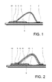
- Fig. 1 shows a side view of a substrate with a chip bonded by a bonding wire before plating according to a first embodiment of the invention
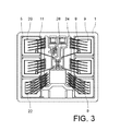
- Fig. 2 shows the arrangement of Fig. 1 after an additional step of depositing a layer of hard metal according to the first embodiment
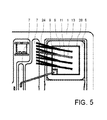
- Fig. 3 shows a schematical view of an entire substrate with multiple semiconductors bonded thereto according to a second embodiment of the invention
- Fig. 4 shows a partial view of the substrate and one power semiconductor as shown in Fig. 3 .
- Fig. 5 shows a partial view of the substrate and the power semiconductor bonded thereon according to a third embodiment of the invention.
- Figs. 1 and 2 illustrate schematically the inventive process for providing a substrate 1 with a power semiconductor 3 mounted thereon, according to a first embodiment.
- the substrate 1 comprises a metalized contact area 5 and a metallization 7, which are both made of a hard metal, which is copper in this embodiment.
- the power semiconductor 3 is soldered to the metalized contact area 5 with one of its surfaces, thereby providing a mechanical and electrical connection to the metalized contact area 5.
- the power semiconductor 3 has a contact pad 9 of aluminum on its top surface 10 opposite to the substrate 1, which is connected by a soft metal bonding means 11 to the metallization 7.
- the soft metal bonding means 11 in this embodiment is a bonding wire 11 made of aluminum and has a diameter of 500 ⁇ m. Accordingly, the substrate 1 with the power semiconductor 3 and aluminum bonding wire 11, as shown in Fig. 1 , can be the result of a conventional bonding method.
- the substrate 1 with the power semiconductor 3 and the bonding wire 11 is then electroplated. Accordingly, the metallization 7 is connected to an electric potential via an auxiliary pin of the substrate 1, which is not shown in the figures.
- ions of hard metal are electrically deposited on the contact pad 9 and the aluminum bonding wire 11, thereby forming a depositing layer 13 thereon, as shown in Fig. 2 .
- the depositing layer 13 is formed of copper with a thickness of 5-200 ⁇ m. Accordingly, the aluminum bonding wire 11 with depositing layer 13 deposited thereon has a diameter of more than 500 ⁇ m, preferably 510-900 ⁇ m. In an alternative embodiment, the depositing layer 13 is formed of nickel.
- the substrate 1 is removed from the depositing bath and the electric potential is disconnected.
- the depositing layer 13 of hard metal is also formed on the metallization 7, since the electric potential is also applied thereto.
- Fig. 3 shows a substrate 1 with multiple power semiconductors 20, 22 mounted thereon, according to a second embodiment of the invention. Since the second embodiment is similar to the first embodiment, same reference numerals are used for like components.
- the power semiconductors 20, 22 in the second embodiment are power transistors 20, e.g. insulated gate bipolar transistors (IGBT), and power diodes 22.
- IGBTs 20 and two power diodes 22 are mounted directly with one of their surfaces to a metalized contact area 5 on the substrate 1 by means of sintering or soldering.
- Two individual metallizations 7 are provided on the substrate 1 and connected by means of aluminum bonding wires 11 as bonding means to the IGBTs 20 and the power diodes 22.
- the aluminum bonding wires 11 in this embodiment have a diameter of 375 ⁇ m.
- the power diodes 22 have one contact pad 9 on their top side 10, which is connected to one of the metallizations 7, whereas the IGBTs 20 have two contact pads 9 corresponding to emitter and gate of the IGBT 20.
- the two contact pads 9 of the IGBT 20 are individually bonded each to one metallization 7.
- the aluminum bonding wires 11 and the contact pad 9 have a depositing layer 13 of hard metal deposited thereon after applying the process described before in respect to the first embodiment.
- the depositing layer 13 in this embodiment is made of copper as described before in respect to the first embodiment and has a thickness of 50-200 ⁇ m.
- Fig. 5 shows a substrate 1 with a power semiconductor 20 mounted thereon according to a third embodiment of the invention. Since the third embodiment is similar to the second embodiment, same reference numerals are used for similar components.
- a substrate 1 is provided with a power transistor 20, in this case an insulated gate bipolar transistor (IGBT), mounted thereon as described before.
- IGBT insulated gate bipolar transistor
- each contact pad 9 of the IGBT 20 is connected to one metallization 7 on the substrate 1 with one aluminum bonding wire 11 as bonding means.
- the depositing step as described above is applied, thereby forming a depositing layer 13 of hard metal on the two aluminum bonding wires 11 and the contact pads 9.
- hard metal bonding means 24 are bonded between the metallization 7 and one contact pad 9 onto the depositing layer 13 of hard metal.
- the hard metal bonding means 24 in this embodiment are bonding wires made of copper.
Landscapes
- Wire Bonding (AREA)
Priority Applications (1)
| Application Number | Priority Date | Filing Date | Title |
|---|---|---|---|
| EP12172513.9A EP2677541A1 (de) | 2012-06-19 | 2012-06-19 | Verfahren zum Drahtbonden eines Leistungshalbleiterbausteins sowie die enstprechende Vorrichtung |
Applications Claiming Priority (1)
| Application Number | Priority Date | Filing Date | Title |
|---|---|---|---|
| EP12172513.9A EP2677541A1 (de) | 2012-06-19 | 2012-06-19 | Verfahren zum Drahtbonden eines Leistungshalbleiterbausteins sowie die enstprechende Vorrichtung |
Publications (1)
| Publication Number | Publication Date |
|---|---|
| EP2677541A1 true EP2677541A1 (de) | 2013-12-25 |
Family
ID=46506151
Family Applications (1)
| Application Number | Title | Priority Date | Filing Date |
|---|---|---|---|
| EP12172513.9A Withdrawn EP2677541A1 (de) | 2012-06-19 | 2012-06-19 | Verfahren zum Drahtbonden eines Leistungshalbleiterbausteins sowie die enstprechende Vorrichtung |
Country Status (1)
| Country | Link |
|---|---|
| EP (1) | EP2677541A1 (de) |
Cited By (5)
| Publication number | Priority date | Publication date | Assignee | Title |
|---|---|---|---|---|
| DE102016107287A1 (de) * | 2016-04-20 | 2017-11-09 | Semikron Elektronik Gmbh & Co. Kg | Leistungshalbleitereinrichtung und Verfahren zum Betrieb einer Leistungshalbleitereinrichtung |
| US11056458B2 (en) | 2018-11-29 | 2021-07-06 | Infineon Technologies Ag | Package comprising chip contact element of two different electrically conductive materials |
| US20220278060A1 (en) * | 2020-12-07 | 2022-09-01 | Infineon Technologies Ag | Molded semiconductor package with high voltage isolation |
| CN116544127A (zh) * | 2023-07-07 | 2023-08-04 | 赛晶亚太半导体科技(浙江)有限公司 | 一种具有大电流的功率器件的制备方法及连接结构 |
| EP4246571A1 (de) * | 2022-03-15 | 2023-09-20 | Kabushiki Kaisha Toshiba | Halbleiterbauelement und verfahren zur herstellung dieses halbleiterbauelements |
Citations (2)
| Publication number | Priority date | Publication date | Assignee | Title |
|---|---|---|---|---|
| DE102005028951A1 (de) * | 2005-06-22 | 2006-12-28 | Infineon Technologies Ag | Anordnung zur elektrischen Verbindung einer Halbleiter-Schaltungsanordnung mit einer äusseren Kontakteinrichtung und Verfahren zur Herstellung derselben |
| JP2009302261A (ja) * | 2008-06-12 | 2009-12-24 | Toyota Central R&D Labs Inc | 半導体装置 |
-
2012
- 2012-06-19 EP EP12172513.9A patent/EP2677541A1/de not_active Withdrawn
Patent Citations (2)
| Publication number | Priority date | Publication date | Assignee | Title |
|---|---|---|---|---|
| DE102005028951A1 (de) * | 2005-06-22 | 2006-12-28 | Infineon Technologies Ag | Anordnung zur elektrischen Verbindung einer Halbleiter-Schaltungsanordnung mit einer äusseren Kontakteinrichtung und Verfahren zur Herstellung derselben |
| JP2009302261A (ja) * | 2008-06-12 | 2009-12-24 | Toyota Central R&D Labs Inc | 半導体装置 |
Non-Patent Citations (1)
| Title |
|---|
| TERASHIMA S ET AL: "Significant reduction of wire sweep using Ni plating to realise ultra fine pitch wire bonding", 2002 PROCEEDINGS 52ND. ELECTRONIC COMPONENTS AND TECHNOLOGY CONFERENCE. ECTC 2002. SAN DIEGO, CA, MAY 28 - 31, 2002; [PROCEEDINGS OF THE ELECTRONIC COMPONENTS AND TECHNOLOGY CONFERENCE], NEW YORK, NY : IEEE, US, vol. CONF. 52, 28 May 2002 (2002-05-28), pages 891 - 896, XP010747737, ISBN: 978-0-7803-7430-0, DOI: 10.1109/ECTC.2002.1008205 * |
Cited By (7)
| Publication number | Priority date | Publication date | Assignee | Title |
|---|---|---|---|---|
| DE102016107287A1 (de) * | 2016-04-20 | 2017-11-09 | Semikron Elektronik Gmbh & Co. Kg | Leistungshalbleitereinrichtung und Verfahren zum Betrieb einer Leistungshalbleitereinrichtung |
| US11056458B2 (en) | 2018-11-29 | 2021-07-06 | Infineon Technologies Ag | Package comprising chip contact element of two different electrically conductive materials |
| US20220278060A1 (en) * | 2020-12-07 | 2022-09-01 | Infineon Technologies Ag | Molded semiconductor package with high voltage isolation |
| US11817407B2 (en) * | 2020-12-07 | 2023-11-14 | Infineon Technologies Ag | Molded semiconductor package with high voltage isolation |
| EP4246571A1 (de) * | 2022-03-15 | 2023-09-20 | Kabushiki Kaisha Toshiba | Halbleiterbauelement und verfahren zur herstellung dieses halbleiterbauelements |
| CN116544127A (zh) * | 2023-07-07 | 2023-08-04 | 赛晶亚太半导体科技(浙江)有限公司 | 一种具有大电流的功率器件的制备方法及连接结构 |
| CN116544127B (zh) * | 2023-07-07 | 2023-09-22 | 赛晶亚太半导体科技(浙江)有限公司 | 一种具有大电流的功率器件的制备方法及连接结构 |
Similar Documents
| Publication | Publication Date | Title |
|---|---|---|
| US8823175B2 (en) | Reliable area joints for power semiconductors | |
| KR101204187B1 (ko) | 소성 접합을 이용한 파워 모듈 및 그 제조 방법 | |
| JP2021061453A (ja) | ワイヤボンドを有するパワーオーバーレイ構造体およびその製造方法 | |
| US10692803B2 (en) | Die embedding | |
| US9613929B2 (en) | Power semiconductor chip with a metallic moulded body for contacting thick wires or strips and method for the production thereof | |
| CN107039364B (zh) | 半导体封装件及其制造方法 | |
| JP6159563B2 (ja) | 少なくとも1つのパワー半導体コンポーネント用の基板を製造するための方法 | |
| US11211373B1 (en) | Double-sided chip stack assembly | |
| EP2677541A1 (de) | Verfahren zum Drahtbonden eines Leistungshalbleiterbausteins sowie die enstprechende Vorrichtung | |
| JPWO2015053356A1 (ja) | 電極接続方法及び電極接続構造 | |
| JP6550477B2 (ja) | 開気孔接触片のガルバニック接合による部品の電気接触方法およびそれに対応する部品モジュール | |
| US20150237718A1 (en) | Power semiconductor device | |
| US9484294B2 (en) | Semiconductor device and method of manufacturing the same | |
| US10229891B2 (en) | Chip embedding package with solderable electric contact | |
| US11462516B2 (en) | Method of manufacturing semiconductor device | |
| US10892253B2 (en) | Semiconductor device manufacturing method and semiconductor device | |
| CN108346587A (zh) | 芯片封装器件及封装方法 | |
| WO2017194661A1 (en) | Power electronic assembly and a low-vibration connection method | |
| WO2017157486A1 (en) | Semiconductor device | |
| US20160351487A1 (en) | Semiconductor device and production method therefor | |
| US10700037B2 (en) | Reinforcement for electrical connectors | |
| EP1995777A1 (de) | Transistorgehäuse mit dielektrischer Isolierung der Waferebene | |
| US11152286B2 (en) | Power semiconductor module device | |
| EP2840607A1 (de) | Halbleitermodul | |
| JP2021044456A (ja) | 半導体装置 |
Legal Events
| Date | Code | Title | Description |
|---|---|---|---|
| PUAI | Public reference made under article 153(3) epc to a published international application that has entered the european phase |
Free format text: ORIGINAL CODE: 0009012 |
|
| AK | Designated contracting states |
Kind code of ref document: A1 Designated state(s): AL AT BE BG CH CY CZ DE DK EE ES FI FR GB GR HR HU IE IS IT LI LT LU LV MC MK MT NL NO PL PT RO RS SE SI SK SM TR |
|
| AX | Request for extension of the european patent |
Extension state: BA ME |
|
| STAA | Information on the status of an ep patent application or granted ep patent |
Free format text: STATUS: THE APPLICATION IS DEEMED TO BE WITHDRAWN |
|
| 18D | Application deemed to be withdrawn |
Effective date: 20140626 |