EP2677597A1 - Antenne et étiquette RFID - Google Patents
Antenne et étiquette RFID Download PDFInfo
- Publication number
- EP2677597A1 EP2677597A1 EP20130167976 EP13167976A EP2677597A1 EP 2677597 A1 EP2677597 A1 EP 2677597A1 EP 20130167976 EP20130167976 EP 20130167976 EP 13167976 A EP13167976 A EP 13167976A EP 2677597 A1 EP2677597 A1 EP 2677597A1
- Authority
- EP
- European Patent Office
- Prior art keywords
- loop
- antenna
- rfid tag
- chip
- chip connection
- Prior art date
- Legal status (The legal status is an assumption and is not a legal conclusion. Google has not performed a legal analysis and makes no representation as to the accuracy of the status listed.)
- Ceased
Links
Images





Classifications
-
- G—PHYSICS
- G06—COMPUTING OR CALCULATING; COUNTING
- G06K—GRAPHICAL DATA READING; PRESENTATION OF DATA; RECORD CARRIERS; HANDLING RECORD CARRIERS
- G06K19/00—Record carriers for use with machines and with at least a part designed to carry digital markings
- G06K19/06—Record carriers for use with machines and with at least a part designed to carry digital markings characterised by the kind of the digital marking, e.g. shape, nature, code
- G06K19/067—Record carriers with conductive marks, printed circuits or semiconductor circuit elements, e.g. credit or identity cards also with resonating or responding marks without active components
- G06K19/07—Record carriers with conductive marks, printed circuits or semiconductor circuit elements, e.g. credit or identity cards also with resonating or responding marks without active components with integrated circuit chips
- G06K19/077—Constructional details, e.g. mounting of circuits in the carrier
- G06K19/07749—Constructional details, e.g. mounting of circuits in the carrier the record carrier being capable of non-contact communication, e.g. constructional details of the antenna of a non-contact smart card
- G06K19/07773—Antenna details
- G06K19/07777—Antenna details the antenna being of the inductive type
- G06K19/07779—Antenna details the antenna being of the inductive type the inductive antenna being a coil
- G06K19/07783—Antenna details the antenna being of the inductive type the inductive antenna being a coil the coil being planar
-
- H—ELECTRICITY
- H01—ELECTRIC ELEMENTS
- H01Q—ANTENNAS, i.e. RADIO AERIALS
- H01Q1/00—Details of, or arrangements associated with, antennas
- H01Q1/12—Supports; Mounting means
- H01Q1/22—Supports; Mounting means by structural association with other equipment or articles
- H01Q1/2208—Supports; Mounting means by structural association with other equipment or articles associated with components used in interrogation type services, i.e. in systems for information exchange between an interrogator/reader and a tag/transponder, e.g. in Radio Frequency Identification [RFID] systems
- H01Q1/2225—Supports; Mounting means by structural association with other equipment or articles associated with components used in interrogation type services, i.e. in systems for information exchange between an interrogator/reader and a tag/transponder, e.g. in Radio Frequency Identification [RFID] systems used in active tags, i.e. provided with its own power source or in passive tags, i.e. deriving power from RF signal
-
- H—ELECTRICITY
- H01—ELECTRIC ELEMENTS
- H01Q—ANTENNAS, i.e. RADIO AERIALS
- H01Q1/00—Details of, or arrangements associated with, antennas
- H01Q1/36—Structural form of radiating elements, e.g. cone, spiral, umbrella; Particular materials used therewith
- H01Q1/38—Structural form of radiating elements, e.g. cone, spiral, umbrella; Particular materials used therewith formed by a conductive layer on an insulating support
-
- H—ELECTRICITY
- H01—ELECTRIC ELEMENTS
- H01Q—ANTENNAS, i.e. RADIO AERIALS
- H01Q7/00—Loop antennas with a substantially uniform current distribution around the loop and having a directional radiation pattern in a plane perpendicular to the plane of the loop
Definitions
- RFID radio frequency identification
- a technique called RFID for identifying and managing individuals has been studied and developed.
- a medium called an RFID tag includes an integrated circuit (IC) chip such as a large scale integration (LSI) chip or the like, and an antenna.
- the RFID tag has a function of transmitting and receiving information, such as identification data of an individual or the like, recorded on the IC chip with the antenna via an electromagnetic wave.
- the information recorded on the IC chip of the RFID tag is read and written by a device called a reader/writer via an electromagnetic wave.
- Types of the above described RFID tag are broadly classified into a passive type and an active type depending on a difference of a power supply method.
- a passive-type RFID tag has advantages such that the tag can be manufactured with less cost than an active-type RFID tag that internally includes a battery, and does not need to be maintained by taking the lifetime of the battery into account.
- the passive-type RFID tag does not include a battery that supplies operating power, power demanded to drive the IC chip needs to be transmitted from the reader/writer to the RFID tag simultaneously with a communication. Accordingly, a communicable distance between the reader/writer and the passive-type RFID tag can be decided according to a distance in which power can be transmitted from the reader/writer to the passive-type RFID tag.
- a frequency band available to a carrier wave is regulated by law or the like since an output of transmitting power is needed for the carrier wave.
- UHF ultra-high frequency
- HF high frequency
- the HF band can be used because the transmission output may be small.
- the UHF band can be used because a transmission output is enabled to be increased.
- the RFID tag needs to be designed to fit a size of a target object to which the RFID tag is attached.
- the RFIG tag needs to be downsized according to the size of the target object to which the RFID tag is attached. Especially, since an antenna occupies most of a mounting area of the RFID tag, the antenna needs to be downsized.
- a length of the antenna becomes shorter than a wavelength corresponding to a desired frequency, and a radiation efficiency of the antenna can be possibly decreased. Therefore, a communicable distance between the reader/writer and the RFID tag can be possibly shortened.
- an RFID tag antenna by including a power feeding terminal to which an LSI chip for an RFID tag is connected, a loop antenna connected to the power feeding terminal, and a bypass conducting path for bypassing a loop of the loop antenna.
- An object of the present invention is to extend a communicable distance between a reader/writer and an RFID tag while downsizing an antenna included in the RFID tag.
- an antenna includes a first loop, a second loop which encloses an outer side of the first loop and is separated from the first loop by a slit and both end of which are merged with both ends of the first loop, and IC chip connection parts provided in a portion where the first loop and the second loop are merged, wherein a loop length of the first loop and a loop length of the second loop are equal to or shorter than one third of a wavelength corresponding to a desired frequency resonant with an IC chip connected to the IC chip connection parts.
- FIG. 1 schematically illustrates a configuration of a loop antenna according to a first embodiment.
- the loop antenna 10 includes a first loop 11, a second loop 12, IC chip connection parts 13a and 13b, and a slit 14.
- the first loop 11 is a loop portion on an inner side in the loop antenna 10
- the second loop 12 is a loop portion on an outer side in the loop antenna 10.
- the first loop 11 is present on an inner side of the second loop 12, and the second loop 12 encloses the outer side of the first loop 11.
- the loop antenna 10 is configured as a double-loop antenna.
- the first loop 11 and the second loop 12 are separated by the slit 14, and merged at the IC chip connection parts 13a and 13b which are positioned at ends of the first loop 11 and the second loop 12. Namely, the first loop 11 and the second loop 12 are connected in parallel when viewed from the IC chip connection parts 13a and 13b.
- the IC chip connection parts 13a and 13b are portions of the loop antenna 10, to which a terminal of an IC chip mounted on the RFID tag is connected.
- the slit 14 is a portion of the loop antenna 10, which is present in a gap between the first loop 11 and the second loop 12, and is a portion that separates the first loop 11 and the second loop 12.
- the first loop 11 and the second loop 12 within the loop antenna 10 take the shape of a quadrangle such as a square or a rectangle except for the IC chip connection parts 13a and 13b which are separately present.
- a length of a side of the second loop 12 that takes the shape of the quadrangle can be 19 mm except for a side on which the IC chip connection parts 13a and 13b are present. Accordingly, the size of the entire RFID tag according to the first embodiment, which includes the loop antenna 10 and the IC chip mounted in the loop antenna 10, can be 19 mm ⁇ 19 mm.
- loop lengths of the first loop 11 and the second loop 12 can be equal to or shorter than 76 mm (19 mm ⁇ 4), and can be approximately one fourth (approximately 0.24 ⁇ ) of 315 mm which is a wavelength ⁇ corresponding to the desired frequency 953 MHz, namely, can be equal to or shorter than one third of 315 mm. That is, the first loop 11 and the second loop 12 within the loop antenna 10 according to the embodiment are very small loops having a loop length that is sufficiently shorter than a wavelength corresponding to a desired frequency. Accordingly, the first loop 11 and the second loop 12 function as an inductor.
- the loop length of the second loop 12 is longer than the loop length of the first loop 11. Accordingly, assuming that the inductors of the first loop 11 and the second loop 12 are respectively La1 and La2, the value of the inductor La2 is larger than the value of the inductor La1, so that a relational expression La2>La1 is satisfied.
- FIG. 2 is a diagram of an equivalent circuit of the RFID tag according to the embodiment.
- the loop antenna 10 according to the first embodiment can be equivalently represented with a circuit where a resistor Ra, the inductor La1 and the inductor La2 are connected in parallel.
- an IC chip 20 mounted on the RFID tag 30 according to the embodiment by being connected to the IC chip connection parts 13a and 13b can be equivalently represented with a circuit where a resistor Rc and a capacitor Cc are connected in parallel.
- a resonant condition of the RFID tag according to the embodiment is that an imaginary component of an admittance Y of the equivalent circuit illustrated in FIG. 2 is zeroed (0), namely, that the following equation (1) is satisfied.
- the value of the resistor Rc and the value of the capacitor Cc are set to 2000 ⁇ and 1.0 pF respectively in the IC chip 20.
- the value of the resistor Ra, the value of the inductor La1, and the value of the inductor La2 are set to 20000 ⁇ , 35nH, and 140nH respectively in the loop antenna 10. If the values are set as described above, a combined inductance of the inductor La1 and the inductor La2 is 28 nH, which satisfies the resonant condition with the capacitor Cc of 1.0 pF at a frequency 953 MHz.
- the value of the inductor La2 is larger than the value of the inductor La1, so that the relational expression La2>La1 is satisfied. Accordingly, the resonant condition represented with the expression (1) can be mainly decided according to the value of the inductor La1. Therefore, the first loop 11 can function as a portion for matching with the IC chip 20 within the loop antenna 10.
- the loop antenna has a characteristic such that the radiation efficiency ⁇ of the loop antenna is highest when a loop length of one circle of the loop antenna is equal to one wavelength ⁇ corresponding to a desired frequency, and the radiation efficiency ⁇ decreases to reduce the antenna gain when the length of one circle of the loop antenna becomes shorter than one wavelength ⁇ .
- the loop length of the second loop antenna 12 is longer than the loop length of the first loop 11 in the loop antenna 10 according to the first embodiment. Accordingly, the radiation efficiency of the second loop antenna 12 is higher than the radiation efficiency of the first loop 11, and the antenna gain is higher. Therefore, the second loop 12 can function as a portion for increasing the antenna gain within the loop antenna 10.
- the shape and the size of the first loop 11 are decided to have an inductance that is resonant with the value of the capacitor Cc of the IC chip to be mounted.
- the loop length of the first loop 11 is decided to satisfy the resonant condition represented with the above described equation (1).
- the shape and the size of the second loop 12 are decided to increase the antenna gain.
- the loop length of one circle of the second loop 12 can be increased as long as possible within a scope of constraints placed by a size of a target object to which the RFIC tag is attached.
- a wire width of the second loop 12 can be increased as thick as possible within the scope of constraints.
- the sizes of the first loop 11 and the second loop 12 are set, for example, in the following steps described below reference to FIG. 3 .
- FIG. 3 illustrates one example of the size of the loop antenna according to the first embodiment.
- the desired frequency is 953 MHz.
- the size demanded for the loop antenna 10 is 19 mm ⁇ 19 mm.
- variations that can occur when the loop antenna 10 is manufactured are ⁇ 0.1 mm.
- an interval between the IC chip connection parts 13a and 13b is 1 mm by taking the size of the IC chip 20 connected to the loop antenna 10 into account.
- the length of each of the sides of the second loop 12 is set to 19mm except for the side on which the IC chip connection parts 13a and 13b are set, as illustrated in FIG. 3 .
- the length of the wire portion in a horizontal direction (X axis direction of FIG. 3 ), on which the IC chip connection parts 13a and 13b are not present is set to 19 mm
- each of lengths of the wire portions in a vertical direction (Y axis direction of FIG. 3 ) is set to 19 mm.
- the length of the wire portion in the horizontal direction, on which the IC chip connection part 13a is present, and the length of the wire portion in the horizontal direction, on which the IC chip connection part 13b is present, are set to 9 mm ((19-1)/2 mm). With such settings, the loop length of one circle of the second loop 12 is increased as long as possible within the scope of constraints placed by the size demanded for the loop antenna 10.
- the width of the slit 14 within the wires in the horizontal direction of the loop antenna 10 among the wire portions of the loop antenna 10 which respectively correspond to the sides of the loop antenna 10 is set to 0.5 mm by taking, into account, precision of the loop antenna 10 when being manufactured. Then, an interval between the slit 14 within the wire adjacent to the IC chip connection part 13a and the slit 14 within the wire adjacent to the IC chip connection part 13b is set to 5 mm. By setting the interval to 5 mm in this way, the length in the horizontal direction of the portion where the first loop 11 and the second loop 12 are merged is set to 2 mm ((5-1)/2mm).
- the length of the wire in the horizontal direction of the first loop 11, on which the IC chip connection parts 13a and 13b are not present, among the wire portions of the first loop 11 which respectively correspond to the sides of the first loop 11, is set to 13 mm.
- the length of the wire in the horizontal direction of the first loop 11, on which the IC chip connection part 13a is present, and the length of the wire in the horizontal direction of the first loop 11, on which the IC chip connection part 13b is present are respectively set to 6 mm ((13-1)/2 mm).
- each of widths of the wires in the horizontal direction of the first loop 11 is set to 1 mm.
- the width of the wire in the horizontal direction of the second loop 12, on which the IC chip connection part 13a is present, and the width of the wire in the horizontal direction of the second loop 12, on which the IC chip connection part 13b is present are set as thick as possible within the scope of constraints. Namely, the widths of these wires are set to 2.5 mm ((19-13-0.5 ⁇ 2/2mm) respectively.
- each width of the slit 14 present within the wires in the horizontal direction of the loop antenna 10 is set to 0.5 mm by taking, into account, the precision of the loop antenna 10 when being manufactured.
- each of the widths of the wires in the vertical direction of the first loop 11 is set to 1 mm.
- each of the widths of the wires in the vertical direction of the second loop 12 is set to 2.5 mm.
- the lengths of the wires in the vertical direction of the first loop 11 are adjusted so that the inductance of the loop antenna 10, namely, the combined inductance of the inductor La1 and the inductor La2 when viewed from the side of the IC chip connection parts 13a and 13b results in 28 nH.
- the width of the wire in the horizontal direction of the second loop 12, on which the IC chip connection parts 13a and 13b are not present, is adjusted.
- starting points of the wires in the vertical direction of the first loop 11 are respectively set at edges, which do not make contact with the second loop 12, among edges of the slit 14 within the wires in the horizontal direction of the loop antenna 10, which are adjacent to the IC chip connection parts 13a and 13b. Then, the lengths of the wires in the vertical direction of the first loop 11 are extended or contracted from the set starting points toward the wire in the horizontal direction of the first loop 11, on which the IC chip connection parts 13a and 13b are not present. Moreover, the width of the wire in the horizontal direction of the second loop 12, on which the IC chip connection parts 13a and 13b are not present, is increased as thick as possible according to the extended or contracted lengths of the wires in the vertical direction of the first loop 11.
- the lengths of the wires in the vertical direction of the first loop 11 are set to 11 mm as illustrated in FIG. 3 .
- the width of the wire in the horizontal direction of the second loop 12, on which the IC chip connection parts 13a and 13b are not preset is set to 4.5 mm ((19-11-0.5 ⁇ 2)-2.5mm).
- the sizes of the first loop 11 and the second loop 12 are set as described above, so that the first loop 11 is made to function as the portion for matching with the IC chip 20 and the second loop 12 is made to function as the portion for increasing the antenna gain in the embodiment.
- the size of the loop antenna 10 and the size setting method which have been described above with reference to FIG. 3 , are merely examples, and are not particularly limited to these examples.
- a material of the loop antenna 10 is a conductor having a conductivity ⁇ of 5 ⁇ 10 6 S/m, and its thickness is 30 ⁇ m.
- FIG. 4 illustrates the shape and the size of the antenna according to the conventional technique to be compared.
- the antenna 40 according to the conventional technique to be compared includes IC chip connection parts 43a and 43b to which the IC chip 20 are connected, a loop part 41 that is connected to the IC chip connection parts and 43b and nearly takes the shape of a quadrangle, and a linear bypass conducting path 42 for bypassing the loop part 41.
- the bypass conducting path 42 is present at a position that divides the vertical direction (Y axis direction of FIG. 4 ) of the loop part 41 into halves.
- the loop part 41 and the bypass conducting path 42 are conductors respectively having a conductivity ⁇ of 5 ⁇ 10 6 S/m, and their thicknesses are 30 ⁇ m. Moreover, a width of each of wires which respectively correspond to sides of the loop part 41 and a width of the bypass conducting path 42 are 2 mm. An interval between the IC chip connection part 43a and the IC chip connection part 43b is 1 mm.
- a length of each of the wires of the loop part 41 is 19 mm except for the wires on which the IC chip connection parts 43a and 43b are present, and a length of the wire on which the IC chip connection part 43a is present and a length of the wire on which the IC chip connection part 43b is present are respectively 9 mm.
- a mounting area of the antenna 40 according to the conventional technique is the same as that of the loop antenna 10 according to the first embodiment to be compared.
- a mounting area of the RFID tag including the antenna 40 is the same as that of the RFID tag including the loop antenna 10.
- the RFID tag including the loop antenna 10 according to the above described first embodiment and the IC chip, and the RFID tag including the conventional antenna 40 and the IC chip 20 are analyzed by using an electromagnetic field simulation by assuming that an output and an antenna gain of the reader/writer are respectively 1W (namely, 30 dBm) and 6 dBi, and minimum operating power P mim of the IC chip is -17 dBm. Results obtained by making a comparison between the performances of both the tags are described below with reference to FIGs. 5 to 9 .
- FIG. 5 illustrates frequency characteristics relative to communicable distances of the RFID tag including the loop antenna according to the first embodiment and the RFID tag including the conventional antenna.
- both the RFID tag including the loop antenna according to the first embodiment and the RFID tag including the conventional antenna satisfy the resonant condition at 953 MHz, so that their communicable distances with the reader/writer become longest.
- the communicable distance of the RFID tag including the conventional antenna 40 is approximately 2 m, whereas that of the RFID tag including the loop antenna 10 according to the first embodiment is approximately 2.5 m as illustrated in FIG. 5 . Accordingly, the communicable distance of the RFID tag including the loop antenna 10 according to the first embodiment can be extended by approximately 25 percent although the mounting area of the RFID tag including the loop antenna 10 according to the first embodiment is the same as that of the RFID tag including the conventional antenna 40.
- the communicable distance of the RFID tag including the loop antenna 10 according to the first embodiment is extended at all frequencies ranging from 800 MHz to 1100 MHz to be measured as a result of the comparison made with the RFID tag including the conventional antenna 40. Accordingly, also at frequencies before and after 953 MHz where the resonant condition is satisfied, the communicable distance of the RFID tag including the loop antenna 10 according to the first embodiment can be extended although its mounting area is the same as that of the RFID tag including the conventional antenna 40.
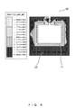
- FIG. 6 illustrates a current density distribution of the RFID tag including the loop antenna according to the first embodiment.
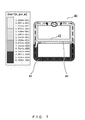
- FIG. 7 illustrates a current density distribution of the RFID tag including the conventional antenna.
- a current concentrates on the first loop 11 which is the loop portion on the inner side, and the first loop 11 functions as an inductor.
- a current concentrates on an inner side loop part 44 which is represented with a dotted line and includes the bypass conducting path 42, and the inner side loop part 44 functions as an inductor.
- a portion of a current path of the inner side loop part 44 and a portion of a current path of the loop part 41 are shared. Therefore, the current flowing into the loop part 41 having a loop length longer by one circle than the inner side loop part 44 is impeded by the current flowing into the inner side loop part 44.
- a current path of the second loop 12 which is a loop portion on the outer side is independent of the current path of the first loop 11 which is a loop portion on the inner side. Therefore, the current flowing into the second loop 12 is not impeded by the current flowing into the first loop 11.
- the second loop 12 having a loop length longer by one circle than the first loop 11 can function as a portion for increasing the antenna gain within the loop antenna 10. Accordingly, since the current flowing into the second loop 12 for increasing an antenna gain flows smoothly without being impeded in the loop antenna 10 according to the first embodiment, the antenna gain can be increased in comparison with the conventional antenna 40.
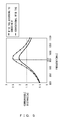
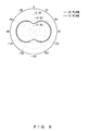
- FIG. 8 illustrates an antenna directivity of the RFID tag including the loop antenna according to the first embodiment.
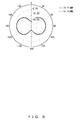
- FIG. 9 illustrates an antenna directivity of the RFID tag including the conventional antenna.
- the antenna gain of the RFID tag including the loop antenna 10 according to the first embodiment increases by approximately 1.7 dB in comparison with the RFID tag including the conventional antenna 40 at any angle on a ZX plane and a YZ plane of coordinate axes illustrated in FIGs. 3 and 4 .
- using the loop antenna 10 according to the first embodiment for an RFID tag enables a communicable distance with a reader/writer to be extended while downsizing the RFID tag.
- the loop antenna 10 according to the first embodiment for an RFID tag enables a communication with a reader/writer to be implemented in a communication distance similar to that of the RFID tag including the conventional antenna even though a transmission output of the reader/writer is suppressed. Accordingly, the RFID tag including the loop antenna 10 is suitable for use in an environment where suppression of unneeded electromagnetic waves is demanded, such as a hospital.
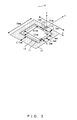
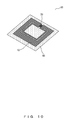
- FIG. 10 illustrates an example of a configuration of the RFID tag according to the embodiment, which includes a tag base.
- FIG. 11 is an explanatory diagram of a usage example of the RFID tag according to the embodiment.
- an antenna pattern of the loop antenna 10 can be formed on a tag base 60 in the form of a sheet, and the IC chip 20 can be mounted on the IC chip connection parts 13a and 13b.
- the tag base 60 can be, for example, polyethylene terephthalate (PET) or paper.
- the loop antenna 10 can be formed by etching a silver (AG) paste, copper (Cu), and aluminum (Al).
- the RFID tag 50 according to the embodiment, which is formed as illustrated in FIG. 10 , can be, for example, pasted onto a cylinder target object 70 as illustrated in FIG. 11 .
- the target object 70 illustrated in FIG. 11 is, for example, a sample container that contains a liquid or the like.
- the loop antenna 10 according to the first embodiment has the maximum antenna gain when an angle from the Z axis is 90 degrees or -90 degrees in the Y axis direction. Moreover, it is proved that the loop antenna 10 according to the first embodiment has the maximum antenna gain when an angle from the Z axis is 90 degrees or -90 degrees in the X axis direction. Accordingly, the RFID tag 50 according to the first embodiment, which includes the loop antenna 10, has an advantage of being insusceptible to influences exerted by the target object 70 because the RFID tag 50 has a constant directivity in its planar direction and has a null point in the vertical direction. In addition, the RFID tag 50 according to the embodiment has an advantage of being attachable to the target object 70 which contains a liquid having a high permittivity, such as a sample container.
- the first loop 11 and the second loop 12 within the loop antenna 10 according to the first embodiment take the shape of a quadrangle such as a square or a rectangle except for the IC chip connection parts 13a and 13b.
- the shapes of the first loop and the second loop of the loop antenna according to the embodiment are not limited to a quadrangle.
- FIG. 12 schematically illustrates a configuration of a loop antenna according to a second embodiment.
- the loop antenna 10' includes a first loop 11', a second loop 12', IC chip connection parts 13a' and 13b', and a slit 14'.
- the first loop 11' and the second loop 12' take the shape of a circle except for the IC chip connection parts 13a' and 13b' that are separately present.
- the first loop 11' is a loop portion on an inners side in the loop antenna 10'
- the second loop 12' is a loop portion on an outer side in the loop antenna 10'.
- the first loop 11' is present on an inner side of the second loop 12'
- the second loop 12' encloses the outer side of the first loop 11'.
- the loop antenna 10' is configured as a double-loop antenna.
- the first loop 11' and the second loop 12' are separated by the slit 14', and merged at the IC chip connection parts 13a and 13b which are positioned at ends of the first loop 11' and the second loop 12'.
- the first loop 11' and the second loop 12' are very small loops having a loop length that is sufficiently shorter than a wavelength corresponding to a desired frequency.
- the first loop 11' can function as a portion for matching with an IC chip connected to the loop antenna 10'.
- the second loop 12' can function as a portion for increasing an antenna gain within the loop antenna 10'. Accordingly, the loop antenna 10' can increase the antenna gain in comparison with a conventional antenna due to reasons similar to those of the loop antenna 10 described above with reference to FIG. 7 .
- loop antenna 10' for an RFID tag enables a communication with a reader/writer to be implemented in a communication distance similar to that of an RFID tag including a conventional antenna even though a transmission output of the reader/writer is suppressed.
Landscapes
- Engineering & Computer Science (AREA)
- Computer Networks & Wireless Communication (AREA)
- Computer Hardware Design (AREA)
- Microelectronics & Electronic Packaging (AREA)
- Physics & Mathematics (AREA)
- General Physics & Mathematics (AREA)
- Theoretical Computer Science (AREA)
- Details Of Aerials (AREA)
- Support Of Aerials (AREA)
Applications Claiming Priority (1)
| Application Number | Priority Date | Filing Date | Title |
|---|---|---|---|
| JP2012140989A JP5928188B2 (ja) | 2012-06-22 | 2012-06-22 | アンテナおよびrfidタグ |
Publications (1)
| Publication Number | Publication Date |
|---|---|
| EP2677597A1 true EP2677597A1 (fr) | 2013-12-25 |
Family
ID=48446142
Family Applications (1)
| Application Number | Title | Priority Date | Filing Date |
|---|---|---|---|
| EP20130167976 Ceased EP2677597A1 (fr) | 2012-06-22 | 2013-05-16 | Antenne et étiquette RFID |
Country Status (3)
| Country | Link |
|---|---|
| US (1) | US9010648B2 (fr) |
| EP (1) | EP2677597A1 (fr) |
| JP (1) | JP5928188B2 (fr) |
Cited By (1)
| Publication number | Priority date | Publication date | Assignee | Title |
|---|---|---|---|---|
| US11322846B2 (en) * | 2019-09-18 | 2022-05-03 | Dongwoo Fine-Chem Co., Ltd. | Antenna device and display device including the same |
Families Citing this family (21)
| Publication number | Priority date | Publication date | Assignee | Title |
|---|---|---|---|---|
| US12595380B2 (en) * | 2007-09-06 | 2026-04-07 | Deka Products Limited Partneship | RFID system and method |
| WO2013145311A1 (fr) * | 2012-03-30 | 2013-10-03 | 富士通株式会社 | Étiquette d'identification par radiofréquence |
| CN205039241U (zh) * | 2014-01-30 | 2016-02-17 | 株式会社村田制作所 | 无线通信装置 |
| DE102016110425B4 (de) * | 2016-06-06 | 2023-07-20 | X-Fab Semiconductor Foundries Gmbh | Halbleitertransformator |
| US11764749B2 (en) | 2016-08-29 | 2023-09-19 | Silicon Laboratories Inc. | Apparatus with partitioned radio frequency antenna and matching network and associated methods |
| US11749893B2 (en) | 2016-08-29 | 2023-09-05 | Silicon Laboratories Inc. | Apparatus for antenna impedance-matching and associated methods |
| US11764473B2 (en) * | 2016-08-29 | 2023-09-19 | Silicon Laboratories Inc. | Apparatus with partitioned radio frequency antenna and matching network and associated methods |
| US11894622B2 (en) | 2016-08-29 | 2024-02-06 | Silicon Laboratories Inc. | Antenna structure with double-slotted loop and associated methods |
| US11769949B2 (en) | 2016-08-29 | 2023-09-26 | Silicon Laboratories Inc. | Apparatus with partitioned radio frequency antenna and matching network and associated methods |
| US10854960B2 (en) * | 2017-05-02 | 2020-12-01 | Richard A. Bean | Electromagnetic energy harvesting devices and methods |
| US11894621B2 (en) | 2017-12-18 | 2024-02-06 | Silicon Laboratories Inc. | Radio-frequency apparatus with multi-band balun with improved performance and associated methods |
| US11894826B2 (en) | 2017-12-18 | 2024-02-06 | Silicon Laboratories Inc. | Radio-frequency apparatus with multi-band balun and associated methods |
| US11916514B2 (en) | 2017-11-27 | 2024-02-27 | Silicon Laboratories Inc. | Radio-frequency apparatus with multi-band wideband balun and associated methods |
| US11750167B2 (en) | 2017-11-27 | 2023-09-05 | Silicon Laboratories Inc. | Apparatus for radio-frequency matching networks and associated methods |
| EP3846499A1 (fr) | 2017-12-14 | 2021-07-07 | GN Hearing A/S | Antenne dipôle à bras multiples pour instrument auditif |
| US10635868B1 (en) * | 2019-01-10 | 2020-04-28 | Samsung Electronics Co., Ltd. | Sensor system using stretchable antenna |
| CN112038744A (zh) * | 2019-06-04 | 2020-12-04 | 深圳市骄冠科技实业有限公司 | 一种天线与芯片平面交叉的射频谐振腔总成及其制备工艺 |
| JP1675741S (fr) * | 2020-05-29 | 2021-01-04 | ||
| US11862872B2 (en) | 2021-09-30 | 2024-01-02 | Silicon Laboratories Inc. | Apparatus for antenna optimization and associated methods |
| JP1734932S (fr) * | 2022-09-07 | 2023-01-19 | ||
| USD1098081S1 (en) * | 2023-11-28 | 2025-10-14 | Checkpoint Systems, Inc. | RFID antenna |
Citations (6)
| Publication number | Priority date | Publication date | Assignee | Title |
|---|---|---|---|---|
| EP1538560A2 (fr) * | 2003-12-04 | 2005-06-08 | Hitachi, Ltd. | Antenne pour l'identification par radiofrequence |
| EP1598815A1 (fr) * | 2004-05-17 | 2005-11-23 | Sony DADC Austria AG | Support de données optiques, procédé et dispositif de production d' un support de données optiques |
| JP2005347798A (ja) | 2004-05-31 | 2005-12-15 | Maspro Denkoh Corp | ループアンテナ及びアンテナ装置 |
| JP2006077645A (ja) | 2004-09-08 | 2006-03-23 | Toyota Motor Corp | 内燃機関の制御装置 |
| WO2009146272A1 (fr) * | 2008-05-29 | 2009-12-03 | Symbol Technologies, Inc. | Antenne insensible à la polarisation pour des lecteurs à identification par radiofréquence manuels |
| EP2133827A1 (fr) * | 2007-04-06 | 2009-12-16 | Murata Manufacturing Co. Ltd. | Dispositif à circuit intégré radio |
Family Cites Families (5)
| Publication number | Priority date | Publication date | Assignee | Title |
|---|---|---|---|---|
| JP4676445B2 (ja) * | 2005-01-24 | 2011-04-27 | 富士通株式会社 | アンテナ及びこれを搭載するrfid用タグ |
| US8508342B2 (en) * | 2009-11-19 | 2013-08-13 | Panasonic Corporation | Transmitting / receiving antenna and transmitter / receiver device using the same |
| JP2011114633A (ja) * | 2009-11-27 | 2011-06-09 | Fujitsu Ltd | アンテナ装置、及びアンテナ装置を含むシステム |
| JP5472322B2 (ja) * | 2009-12-24 | 2014-04-16 | 旭硝子株式会社 | Rfidタグ |
| JP5459126B2 (ja) * | 2010-07-16 | 2014-04-02 | 富士通株式会社 | アンテナシート、タグ及びタグ製造方法 |
-
2012
- 2012-06-22 JP JP2012140989A patent/JP5928188B2/ja not_active Expired - Fee Related
-
2013
- 2013-05-16 US US13/895,622 patent/US9010648B2/en active Active
- 2013-05-16 EP EP20130167976 patent/EP2677597A1/fr not_active Ceased
Patent Citations (6)
| Publication number | Priority date | Publication date | Assignee | Title |
|---|---|---|---|---|
| EP1538560A2 (fr) * | 2003-12-04 | 2005-06-08 | Hitachi, Ltd. | Antenne pour l'identification par radiofrequence |
| EP1598815A1 (fr) * | 2004-05-17 | 2005-11-23 | Sony DADC Austria AG | Support de données optiques, procédé et dispositif de production d' un support de données optiques |
| JP2005347798A (ja) | 2004-05-31 | 2005-12-15 | Maspro Denkoh Corp | ループアンテナ及びアンテナ装置 |
| JP2006077645A (ja) | 2004-09-08 | 2006-03-23 | Toyota Motor Corp | 内燃機関の制御装置 |
| EP2133827A1 (fr) * | 2007-04-06 | 2009-12-16 | Murata Manufacturing Co. Ltd. | Dispositif à circuit intégré radio |
| WO2009146272A1 (fr) * | 2008-05-29 | 2009-12-03 | Symbol Technologies, Inc. | Antenne insensible à la polarisation pour des lecteurs à identification par radiofréquence manuels |
Cited By (1)
| Publication number | Priority date | Publication date | Assignee | Title |
|---|---|---|---|---|
| US11322846B2 (en) * | 2019-09-18 | 2022-05-03 | Dongwoo Fine-Chem Co., Ltd. | Antenna device and display device including the same |
Also Published As
| Publication number | Publication date |
|---|---|
| JP5928188B2 (ja) | 2016-06-01 |
| JP2014007504A (ja) | 2014-01-16 |
| US20130341411A1 (en) | 2013-12-26 |
| US9010648B2 (en) | 2015-04-21 |
Similar Documents
| Publication | Publication Date | Title |
|---|---|---|
| EP2677597A1 (fr) | Antenne et étiquette RFID | |
| US7570225B2 (en) | Antenna and non-contact tag | |
| US7183994B2 (en) | Compact antenna with directed radiation pattern | |
| CN102144332B (zh) | Rfid标签、rfid标签组件及rfid系统 | |
| EP3196808B1 (fr) | Unité de terminal de communication d'informations sans contact, dispositif de type carte, téléphone portable et dispositif pouvant être porté | |
| US10917137B2 (en) | NFC antenna in a mobile device | |
| JP5444507B2 (ja) | アンテナ、無線タグ、及び、アンテナの製造方法 | |
| EP2448064A1 (fr) | Dispositif de communication radio | |
| US9703997B2 (en) | RFID tag and RFID system | |
| JP2014533057A (ja) | アンテナ構造体、及びアンテナ構造体を備えるrfidトランスポンダシステム | |
| Faudzi et al. | A compact dipole UHF-RFID tag antenna | |
| El Hachimi et al. | A compact dual-band antenna including symmetrical slots for 2.45/5.8 GHz handheld RFID reader applications | |
| JP2011130254A (ja) | 無線通信装置 | |
| CN104466353B (zh) | 超带宽可集成读写器电路模块的uhf频段rfid读写器天线 | |
| Wickramasinghe et al. | Design of a passive rfid tag antenna with a modified t-match structure | |
| JP5400945B1 (ja) | アンテナの製造方法 | |
| WO2013011703A1 (fr) | Antenne et étiquette sans fil | |
| Nguyen et al. | Novel design of RFID UHF passive tag for wideband applications by direct and contactless chip connection | |
| Tan et al. | Compact dual band tag antenna design for radio frequency identification (RFID) application | |
| KR101720688B1 (ko) | 마이크로스트립 안테나 | |
| Choo et al. | Three label tags for special applications: attaching on small targets, long distance recognition, and stable performance with arbitrary objects | |
| JP2018160736A (ja) | 非接触型データ受送信体 | |
| Sofi et al. | Antenna Design for UHF RFID Tags Using Two Coupled Patches | |
| Kimouche et al. | New dipole slot antenna design for RFID communications | |
| CN103682647A (zh) | 用于无线射频的偶极天线 |
Legal Events
| Date | Code | Title | Description |
|---|---|---|---|
| PUAI | Public reference made under article 153(3) epc to a published international application that has entered the european phase |
Free format text: ORIGINAL CODE: 0009012 |
|
| AK | Designated contracting states |
Kind code of ref document: A1 Designated state(s): AL AT BE BG CH CY CZ DE DK EE ES FI FR GB GR HR HU IE IS IT LI LT LU LV MC MK MT NL NO PL PT RO RS SE SI SK SM TR |
|
| AX | Request for extension of the european patent |
Extension state: BA ME |
|
| 17P | Request for examination filed |
Effective date: 20140325 |
|
| RBV | Designated contracting states (corrected) |
Designated state(s): AL AT BE BG CH CY CZ DE DK EE ES FI FR GB GR HR HU IE IS IT LI LT LU LV MC MK MT NL NO PL PT RO RS SE SI SK SM TR |
|
| 17Q | First examination report despatched |
Effective date: 20160428 |
|
| STAA | Information on the status of an ep patent application or granted ep patent |
Free format text: STATUS: THE APPLICATION HAS BEEN REFUSED |
|
| 18R | Application refused |
Effective date: 20170628 |