EP2677604A2 - Dispositif de prise d'oreille à angle réglable - Google Patents
Dispositif de prise d'oreille à angle réglable Download PDFInfo
- Publication number
- EP2677604A2 EP2677604A2 EP13173135.8A EP13173135A EP2677604A2 EP 2677604 A2 EP2677604 A2 EP 2677604A2 EP 13173135 A EP13173135 A EP 13173135A EP 2677604 A2 EP2677604 A2 EP 2677604A2
- Authority
- EP
- European Patent Office
- Prior art keywords
- ear jack
- angle
- unit
- elastic member
- ear
- Prior art date
- Legal status (The legal status is an assumption and is not a legal conclusion. Google has not performed a legal analysis and makes no representation as to the accuracy of the status listed.)
- Granted
Links
Images





Classifications
-
- H—ELECTRICITY
- H01—ELECTRIC ELEMENTS
- H01R—ELECTRICALLY-CONDUCTIVE CONNECTIONS; STRUCTURAL ASSOCIATIONS OF A PLURALITY OF MUTUALLY-INSULATED ELECTRICAL CONNECTING ELEMENTS; COUPLING DEVICES; CURRENT COLLECTORS
- H01R13/00—Details of coupling devices of the kinds covered by groups H01R12/70 or H01R24/00 - H01R33/00
- H01R13/60—Means for supporting coupling part when not engaged
-
- H—ELECTRICITY
- H01—ELECTRIC ELEMENTS
- H01R—ELECTRICALLY-CONDUCTIVE CONNECTIONS; STRUCTURAL ASSOCIATIONS OF A PLURALITY OF MUTUALLY-INSULATED ELECTRICAL CONNECTING ELEMENTS; COUPLING DEVICES; CURRENT COLLECTORS
- H01R24/00—Two-part coupling devices, or either of their cooperating parts, characterised by their overall structure
- H01R24/58—Contacts spaced along longitudinal axis of engagement
-
- H—ELECTRICITY
- H01—ELECTRIC ELEMENTS
- H01R—ELECTRICALLY-CONDUCTIVE CONNECTIONS; STRUCTURAL ASSOCIATIONS OF A PLURALITY OF MUTUALLY-INSULATED ELECTRICAL CONNECTING ELEMENTS; COUPLING DEVICES; CURRENT COLLECTORS
- H01R35/00—Flexible or turnable line connectors, i.e. the rotation angle being limited
- H01R35/04—Turnable line connectors with limited rotation angle with frictional contact members
-
- H—ELECTRICITY
- H01—ELECTRIC ELEMENTS
- H01R—ELECTRICALLY-CONDUCTIVE CONNECTIONS; STRUCTURAL ASSOCIATIONS OF A PLURALITY OF MUTUALLY-INSULATED ELECTRICAL CONNECTING ELEMENTS; COUPLING DEVICES; CURRENT COLLECTORS
- H01R2201/00—Connectors or connections adapted for particular applications
- H01R2201/16—Connectors or connections adapted for particular applications for telephony
Definitions
- the present disclosure relates to an ear jack device used in an electronic device. More particularly, the present disclosure relates to an angle adjustable ear jack device capable of adjusting an angle of the ear jack.
- the electronic device In order to make a sound or transmit sound to a user through an external speaker such as an earphone or a headphone instead of a built-in speaker in an electronic device, the electronic device requires an ear jack.
- the ear jack is a device for connecting a plug of an external device (e.g., an earphone) to the electronic device.
- the plug is generally a metal portion for transmitting and receiving a sound signal and/or an electric signal between the electronic device and the earphone.
- the earphone plug when the earphone plug is inserted into the ear jack, by contacting with the metal portion within the ear jack, the earphone plug transfers an electric signal including a sound signal of the electronic device to an earphone or transfers a sound signal and an electric signal of the earphone through, for example a built-in microphone of the earphone to the electronic device.
- the metal portion for transferring an electric signal can be built into an ear jack by an insert injection method.
- PCB Printed Circuit Board
- SMD Surface-Mount Device
- FPCB Flexible Printed Circuit Board
- FIGS. 1A and 1B are perspective views illustrating an ear jack mounted at one surface of a PCB by using the SMD according to the related art.
- the conventional ear jack 12 cannot be moved in any direction because it is fixed to the PCB.
- the angle of an earphone plug 20 cannot be adjusted to correspond to a design shape or the external appearance of the electronic device. For instance, when the electronic device is designed as having a rounded-shape surface 30, the earphone plug 20 is still horizontally inserted into the ear jack 12. Even though the earphone plug 20 is completely inserted into the ear jack 12, a portion of the earphone plug 22 remains exposed to the outside.
- a user can misunderstand that the earphone plug 20 is not completely inserted into the ear jack 12 and thus the user may forcibly further push the earphone plug 20 into the ear jack 12.
- the forcible insertion components can be damaged and malfunction may occur.
- FIGS. 2A and 2B are perspective views illustrating an obliquely mounted ear jack having a separate FPCB 14 according to the related art.
- FIGS. 2A and 2B illustrate a state in which an insertion angle of the ear jack 12 is inclined to correspond to an external appearance or design (e.g., a rounded-shape surface design) of an electronic device as an alternative for addressing the problem described with reference to FIGS. 1A and 1B .
- an external appearance or design e.g., a rounded-shape surface design
- FIGS. 1A and 1B illustrate a state in which an insertion angle of the ear jack 12 is inclined to correspond to an external appearance or design (e.g., a rounded-shape surface design) of an electronic device as an alternative for addressing the problem described with reference to FIGS. 1A and 1B .
- an external appearance or design e.g., a rounded-shape surface design
- an aspect of the present disclosure is to provide an angle adjustable ear jack device that can adjust the insertion angle of an earphone plug according to an external appearance or design of an electronic device.
- Another aspect of the present disclosure is to prevent components from being damaged and causing malfunctions as a result of unnecessary further forcible insertion.
- Another aspect of the present disclosure is to provide an angle adjustable ear jack device that enhances the capability of sharing components and reducing production costs of the electronic device through standardization of an ear jack.
- an angle adjustable ear jack device includes an ear jack unit capable of an angle adjustment, an ear jack support unit for adjusting the angle of the ear jack unit, and at least one hinge for assembling the ear jack unit and the ear jack support unit.
- two or more fixing portions are positioned at both sides of the ear jack, and the fixing portion is bonded to an angle adjustment hole positioned at the ear jack support and fixes an angle of the ear jack.
- the conductive elastic member maintains a contact with the land pad, and the length of the conductive elastic member increases or decreases according to a change in an angle of the ear jack.
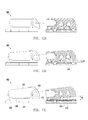
- FIGS. 1A and 1B are perspective views illustrating an example of mounting an ear jack in one surface of a Printed Circuit Board (PCB) according to the related art;
- FIGS. 2A and 2B are perspective views illustrating an example of obliquely mounting an ear jack to a Flexible Printed Circuit Board (FPCB) by using a separate FPCB according to the related art;
- FPCB Flexible Printed Circuit Board
- FIGS. 3A and 3B are perspective views illustrating an ear jack and a fixing portion according to an exemplary embodiment of the present disclosure
- FIG. 4 is a perspective view illustrating a conductive elastic member and a metal portion that transfer an electric signal to other devices or to a land pad according to an exemplary embodiment of the present disclosure
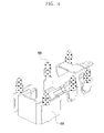
- FIG. 5 is a perspective view illustrating an ear jack unit in which an ear jack, a fixing portion, a conductive elastic member, and a metal portion are assembled together in relation to FIGS. 3A and 3B and FIG. 4 according to an exemplary embodiment of the present disclosure;
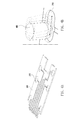
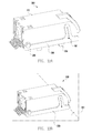
- FIGS. 6A and 6B are perspective views illustrating a land pad and a contact land that transfer an electric signal of an ear jack to a PCB according to an exemplary embodiment of the present disclosure
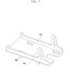
- FIG. 7 is a perspective view illustrating an ear jack plate to be disposed at a PCB according to an exemplary embodiment of the present disclosure
- FIG. 8 is a perspective view illustrating an ear jack support unit in which an ear jack plate and a land pad are assemble together in relation to FIGS. 6A and 6B and FIG. 7 according to an exemplary embodiment of the present disclosure
- FIGS. 9A and 9B are exploded perspective views illustrating an ear jack unit and an ear jack support unit assembled by a hinge in relation to FIG. 3A to FIG. 8 according to an exemplary embodiment of the present disclosure
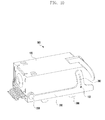
- FIG. 10 is a perspective view illustrating an angle adjustable ear jack device in which an ear jack unit and an ear jack support unit are assembled in relation to FIGS. 9A and 9B according to an exemplary embodiment of the present disclosure
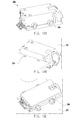
- FIGS. 11A to 11C are cross-sectional views illustrating change in an angle of an angle adjustable ear jack device mounted in a PCB according to an exemplary embodiment of the present disclosure
- FIGS. 12A and 12B are perspective views illustrating an angle adjustable ear jack device in an on-board type according to an exemplary embodiment of the present disclosure
- FIGS. 13A to 13C are perspective views illustrating an angle adjustable ear jack device mounted in a PCB-cutting type according to an exemplary embodiment of the present disclosure.
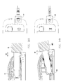
- FIGS. 14A and 14B are cross-sectional views and plan views comparing an exposure level of an earphone plug after insertion according to an exemplary embodiment of the present disclosure.
- the following exemplary embodiments illustrate an earphone plug, however, the scope of the present disclosure is not limited to the earphone plug and can be applied to entire devices having a plug that can transmit and receive a sound signal and/or an electric signal with the ear jack.
- a shape of components including an ear jack unit, an ear jack support unit, a fixing portion, and a hinge used in exemplary embodiments of the present invention are merely exemplary, and thus the present disclosure is not limited thereto.
- FIGS. 3A and 3B are perspective views illustrating an ear jack and a fixing portion according to an exemplary embodiment of the present disclosure.
- the fixing portion 102 is used for fixing an angle of the ear jack 100 according to an external appearance or design of an electronic device.
- a position of the fixing portion 102 is not limited to one location of the ear jack 100 and may be changed to, or positioned at, various locations as needed.
- the fixing portion 102 may comprise various fixing members including a pogo pin. Further, the shape of the fixing portion 102 is not limited to the shape described in FIGS. 3A and 3B . In exemplary embodiments, a variety of shapes can be used.
- FIG. 4 is a perspective view illustrating a conductive elastic member and a metal portion that transfer an electric signal to other devices or to a land pad according to an exemplary embodiment of the present disclosure.
- the conductive elastic member 106 and the metal portion 104 shown in FIG. 4 can be housed within the ear jack by an insert injection molding method.
- the conductive elastic member 106 includes a pogo pin and may be formed with various members having conductivity and an elastic force. The length of the conductive elastic member 106 increases or decreases according to change in a pressure and/or an angle applied to the ear jack 100.
- FIG. 5 is a perspective view illustrating an ear jack unit in which an ear jack, a fixing portion, a metal portion, and a conductive elastic member are assembled together in relation to FIGS. 3A and 3B and FIG. 4 according to an exemplary embodiment of the present disclosure.
- the fixing portion 102, the metal portion 104, and the conductive elastic member 106 can be housed in the ear jack 100 of the ear jack unit 120 by using an insert injection molding method.
- FIGS. 6A and 6B are perspective views illustrating a land pad and a contact land that transfer an electric signal of the ear jack to a Printed Circuit Board (PCB) according to an exemplary embodiment of the present disclosure.
- PCB Printed Circuit Board
- a contact land 210 for maintaining a contact with the conductive elastic member 106 in relation to FIG. 5 is shown.
- the land pad 208 shown in FIG. 6A performs a function of transferring an electric signal of the ear jack unit 120 to the PCB or transferring a sound signal and/or an electric signal generated in an electronic device to the ear jack unit 120 shown in FIG. FIG. 5 .
- the land pad 208 includes a plurality of contact lands 210.
- the conductive elastic member 106 housed in the ear jack 100 maintains contact with the contact land 210 even if an angle of the ear jack unit 120 is changed.
- the contact land 210 may have a characteristic of being extended in a lengthwise direction.
- the length of the conductive elastic member 106 may increase or decrease.
- Contact of the elastic member 106 and the contact land 210 moves in a direction depicted by the arrow shown in FIG. 6B , thereby maintaining a stable and continuous contact between the conductive elastic member 106 and the contact land 210.
- FIG. 7 is a perspective view illustrating an ear jack plate to be disposed at a PCB according to an exemplary embodiment of the present disclosure.
- the ear jack plate 200 is generally made of a Sustain (SUS) press with a metal material and corresponds to a frame in which the ear jack unit 120 is assembled.
- the ear jack plate 200 may have at least one mounting portion 204 that would be used to mount the ear jack plate in the PCB using a Surface Mount Device (SMD).
- SMD Surface Mount Device
- the position and shape of the mounting portion 204 may be changed according to a type (e.g., on-board or pc-cutting type) as described later.
- the ear jack plate 200 may have an angle adjustment hole 202 for adjusting an angle of the ear jack unit 120 by bonding to the fixing portion 102 positioned at both side of the ear jack 100.
- a distance, a size, and the number of the angle adjustment hole 202 may be changed according to a product.
- the shape of the adjustment hole is not limited to the shape described in FIG. 7 . Its shape can be modified in accordance with the shape of the fixing portion 102.
- FIG. 8 is a perspective view illustrating an ear jack support unit in which an ear jack plate and a land pad are assemble together in relation to FIGS. 6A and 6B and FIG. 7 according to an exemplary embodiment of the present invention.
- ear jack plate 200 of ear jack support unit 220 and land pad 208 are shown as assembled according to an exemplary embodiment of the present disclosure.
- FIGS. 9A and 9B are exploded perspective views illustrating an ear jack unit and an ear jack support unit assembled by a hinge in relation to FIGS. 3A to FIG. 8 according to an exemplary embodiment of the present disclosure.
- the hinge 206 functions as a rotation axis when an angle of the ear jack unit 120 is changed.
- the hinge 206 is inserted into a hinge hole 108 of the ear jack unit 120.
- FIG. 10 is a perspective view illustrating an angle adjustable ear jack device in which an ear jack unit and an ear jack support unit are assembled in relation to FIGS. 9A and 9B according to an exemplary embodiment of the present disclosure.
- the ear jack unit 120 and the ear jack support unit 220 are coupled by the hinge 206, and the fixing portion 102 is bonded to the angle adjustment hole 202 of the ear jack plate 200 having mounting portion 204.
- FIGS. 11A to 11C are cross-sectional views illustrating change in an angle of the angle adjustable ear jack device mounted in a PCB according to an exemplary embodiment of the present disclosure.
- FIG. 11A illustrates an angle adjustable ear jack device 300 mounted in a PCB 201 in a horizontal state.
- FIG. 11B illustrates an ear jack unit 120 with an angle R1 compared with FIG. 11A.
- FIG. 11C illustrates the ear jack unit 120 with an increased angle R2 compared with FIG. 11B .
- the ear jack unit 120 rotates in a center of the hinge 206 of the ear jack plate 200.
- the fixing portion 102 fixes an angle of the ear jack unit 120 by bonding to the angle adjustment hole 202 in correspondence with the angle (e.g., R1 and R2).
- FIG. 11B shows the angle adjustable ear jack device with a certain angle (R1).
- the fixing portion 102 is bonded to an angle adjustment hole which is different from the adjustment hole depicted in FIG. 11A.
- FIG. 11C illustrates an exemplary embodiment that has a bigger angle (R2) than the angle R1 in FIG. 11B .
- the fixing portion 102 is bonded to a different angle adjustment hole in correspondence with the angle R2.
- FIGS. 11A to 11C also illustrate change in the length of the conductive elastic member 106 in accordance with the angle change of the ear jack unit 120 according to exemplary embodiments of the present disclosure.
- the conductive elastic member 106 continues to maintain a contact with the contact land 210.
- an angle of the ear jack unit 120 changes from R2 to R1
- the length of the conductive elastic member 106 may decrease in accordance with the angle change.
- FIGS. 12A and 12B are perspective views illustrating an angle adjustable ear jack device mounted in an on-board type according to an exemplary embodiment of the present disclosure.
- an exemplary angle adjustable ear jack device 300 is described below in connection with FIGS. 13A to 13C .
- FIGS. 13A to 13C are perspective views illustrating an angle adjustable ear jack device mounted in a PCB-cutting type according to an exemplary embodiment of the present disclosure.
- FIGS. 12A and 13A to 13C when comparing FIG. 12A and FIG. 13A , the positions and shapes of the mounting portion 204 are different. That is, a method of mounting the angle adjustable ear jack device 300 in the PCB 201 may vary depending on the design and thickness of an electronic device. In this case, a position and a shape of the mounting portion 204 may be changed according to a method of mounting the angle adjustable ear jack device 300 in the PCB 201.
- FIG. 13B illustrates an example of a PC-cutting type that positions the angle adjustable ear jack device 300 in between the PCB by cutting a specific portion of the PCB 201.
- FIG. 13B illustrates an example of a PC-cutting type that positions the angle adjustable ear jack device 300 in between the PCB by cutting a specific portion of the PCB 201.
- FIG. 13C illustrates a rear view of the PCB where the angle adjustable ear jack device 300 mounted in the PC-cutting type.
- the method of mounting in the PCB 201 of the angle adjustable ear jack device 300 is not limited to the on-board and PC-cutting type.
- FIGS. 14A and 14B are cross-sectional views and plan views comparing an exposure amount of an earphone plug after insertion according to an exemplary embodiment of the present disclosure.
- FIG. 14A an earphone plug exposure D1 exposed to the outside when the earphone plug 20 is inserted into the conventional jack 12 is shown.
- FIG. 14B shows an earphone plug exposure D2 exposed to the outside when an earphone plug 400 is inserted into the angle adjustable ear jack device 300 according to an exemplary embodiment of the present disclosure.
- a mounting angle of the ear jack 100 may be adjusted to correspond to an external appearance or design (e.g., a rounded surface design) of an electronic device, thereby minimizing the amount of the earphone plug exposure exposed to the outside.
- exemplary embodiments of the present disclosure prevent a user's misunderstanding that the earphone plug 400 is not completely inserted into the ear jack 100. Consequently, it can prevent components from being damaged and malfunction from occurring as a result of the forcible insertion.
- an ear jack component may be standardized, and sharing of the ear jack can be enhanced. Further, by using one type of ear jack device in electronic devices having various designs, and without changing the ear jack according to an external appearance or design (e.g., a curved surface design) of an electronic device, the mounting ability of the ear jack may be enhanced and production costs may be reduced.
- an external appearance or design e.g., a curved surface design
Landscapes
- Coupling Device And Connection With Printed Circuit (AREA)
- Headphones And Earphones (AREA)
- Telephone Set Structure (AREA)
Applications Claiming Priority (1)
| Application Number | Priority Date | Filing Date | Title |
|---|---|---|---|
| KR1020120066818A KR20130143339A (ko) | 2012-06-21 | 2012-06-21 | 각도조절 이어잭 모듈 |
Publications (3)
| Publication Number | Publication Date |
|---|---|
| EP2677604A2 true EP2677604A2 (fr) | 2013-12-25 |
| EP2677604A3 EP2677604A3 (fr) | 2015-02-25 |
| EP2677604B1 EP2677604B1 (fr) | 2016-11-16 |
Family
ID=48700331
Family Applications (1)
| Application Number | Title | Priority Date | Filing Date |
|---|---|---|---|
| EP13173135.8A Not-in-force EP2677604B1 (fr) | 2012-06-21 | 2013-06-21 | Dispositif de prise d'oreille à angle réglable |
Country Status (4)
| Country | Link |
|---|---|
| US (1) | US9219330B2 (fr) |
| EP (1) | EP2677604B1 (fr) |
| KR (1) | KR20130143339A (fr) |
| CN (1) | CN103515821B (fr) |
Cited By (2)
| Publication number | Priority date | Publication date | Assignee | Title |
|---|---|---|---|---|
| WO2015148419A3 (fr) * | 2014-03-27 | 2015-12-10 | Microsoft Technology Licensing, Llc | Connecteurs de dispositif informatique |
| WO2019184448A1 (fr) * | 2018-03-30 | 2019-10-03 | 无锡睿勤科技有限公司 | Prise de casque d'écoute |
Families Citing this family (10)
| Publication number | Priority date | Publication date | Assignee | Title |
|---|---|---|---|---|
| DE102012210921A1 (de) * | 2012-06-27 | 2014-01-23 | Robert Bosch Gmbh | Kontaktelement zum Verbinden mit einer Leiterplatte, Kontaktsystem und Verfahren |
| CN105337090B (zh) * | 2014-06-09 | 2018-03-06 | 富士康(昆山)电脑接插件有限公司 | 电连接器组件 |
| CN204144492U (zh) * | 2014-08-22 | 2015-02-04 | 富士康(昆山)电脑接插件有限公司 | 插座连接器 |
| CN108616020B (zh) * | 2016-12-12 | 2020-09-29 | 富士康(昆山)电脑接插件有限公司 | 电连接器 |
| CN108616021B (zh) * | 2016-12-12 | 2020-04-24 | 富士康(昆山)电脑接插件有限公司 | 电连接器 |
| CN108281811A (zh) * | 2018-01-15 | 2018-07-13 | 珠海太川云社区技术股份有限公司 | 可改变网口角度的室内机 |
| CN108493649A (zh) * | 2018-03-14 | 2018-09-04 | 郑州云海信息技术有限公司 | 一种非定向可调连接器 |
| CN208797230U (zh) * | 2018-08-29 | 2019-04-26 | 富鼎精密工业(郑州)有限公司 | 电连接器 |
| CN109361087A (zh) * | 2018-11-16 | 2019-02-19 | 苏州三星电子电脑有限公司 | 高度可调接口装置及其构成的多媒体设备 |
| CN112952414B (zh) * | 2021-01-27 | 2022-11-25 | 维沃移动通信有限公司 | 电子设备 |
Family Cites Families (21)
| Publication number | Priority date | Publication date | Assignee | Title |
|---|---|---|---|---|
| US4099823A (en) * | 1977-03-18 | 1978-07-11 | Bell Telephone Laboratories, Incorporated | High density multipair cable connecting block |
| JPH02117596U (fr) * | 1989-03-10 | 1990-09-20 | ||
| US5639261A (en) * | 1994-12-23 | 1997-06-17 | Lucent Technologies Inc. | Modular cross-connect system |
| JPH10302863A (ja) * | 1997-04-25 | 1998-11-13 | Molex Inc | 基板取付型電気コネクタ |
| US6537106B1 (en) * | 1998-06-05 | 2003-03-25 | Adc Telecommunications, Inc. | Telecommunications patch panel with angled connector modules |
| JP2005093219A (ja) * | 2003-09-17 | 2005-04-07 | Kyocera Corp | 外部端子構造 |
| KR100619969B1 (ko) | 2004-12-13 | 2006-09-08 | 엘지전자 주식회사 | 휴대 단말기의 이어잭 |
| US7455548B2 (en) * | 2006-10-19 | 2008-11-25 | Adc Telecommunication, Inc. | Rotatable connector modules with inverted jacks |
| US7335056B1 (en) * | 2006-10-19 | 2008-02-26 | Adc Telecommunications, Inc. | RJ to RJ swing panel |
| SG150428A1 (en) * | 2007-09-06 | 2009-03-30 | Adc Gmbh | Telecommunications patch panel |
| CN101754606B (zh) * | 2008-12-04 | 2013-05-29 | 深圳富泰宏精密工业有限公司 | 电子装置 |
| US7942705B2 (en) * | 2009-03-20 | 2011-05-17 | Apple Inc. | Audio jack with pogo pins for conductive contacts |
| US7874869B2 (en) * | 2009-03-26 | 2011-01-25 | Cisco Technology, Inc. | Reconfigurable patch panel |
| DE202009011478U1 (de) | 2009-08-26 | 2010-02-11 | Sennheiser Electronic Gmbh & Co. Kg | Hörer und Adapter |
| KR101719302B1 (ko) | 2010-01-08 | 2017-03-23 | 삼성전자주식회사 | 이어플러그 인식을 위한 이어잭 |
| US8123569B2 (en) * | 2010-02-08 | 2012-02-28 | Hon Hai Precision Ind. Co., Ltd. | Waterproof audio jack connector |
| JP5806313B2 (ja) * | 2010-08-25 | 2015-11-10 | カーディアック ペースメイカーズ, インコーポレイテッド | 埋込型装置のハウジングへのヘッダ取付装置および方法 |
| JP2012065009A (ja) * | 2010-09-14 | 2012-03-29 | Smk Corp | 電子機器の接続ジャック部の取付構造 |
| CN201868637U (zh) | 2010-11-03 | 2011-06-15 | 华为终端有限公司 | 一种耳机座及带有耳机座的电子产品 |
| EP2535986B1 (fr) | 2010-12-17 | 2014-02-26 | BlackBerry Limited | Prise jack pour un dispositif électronique portable |
| US8287314B1 (en) * | 2011-08-03 | 2012-10-16 | Cheng Uei Precision Industry Co., Ltd. | Audio jack connector |
-
2012
- 2012-06-21 KR KR1020120066818A patent/KR20130143339A/ko not_active Ceased
-
2013
- 2013-06-20 CN CN201310247363.0A patent/CN103515821B/zh not_active Expired - Fee Related
- 2013-06-20 US US13/922,480 patent/US9219330B2/en not_active Expired - Fee Related
- 2013-06-21 EP EP13173135.8A patent/EP2677604B1/fr not_active Not-in-force
Non-Patent Citations (1)
| Title |
|---|
| None |
Cited By (3)
| Publication number | Priority date | Publication date | Assignee | Title |
|---|---|---|---|---|
| WO2015148419A3 (fr) * | 2014-03-27 | 2015-12-10 | Microsoft Technology Licensing, Llc | Connecteurs de dispositif informatique |
| US9306344B2 (en) | 2014-03-27 | 2016-04-05 | Microsoft Technology Licensing, Llc | Computing device connectors |
| WO2019184448A1 (fr) * | 2018-03-30 | 2019-10-03 | 无锡睿勤科技有限公司 | Prise de casque d'écoute |
Also Published As
| Publication number | Publication date |
|---|---|
| US20130344732A1 (en) | 2013-12-26 |
| EP2677604B1 (fr) | 2016-11-16 |
| CN103515821B (zh) | 2017-05-10 |
| EP2677604A3 (fr) | 2015-02-25 |
| KR20130143339A (ko) | 2013-12-31 |
| CN103515821A (zh) | 2014-01-15 |
| US9219330B2 (en) | 2015-12-22 |
Similar Documents
| Publication | Publication Date | Title |
|---|---|---|
| US9219330B2 (en) | Angle adjustable ear jack device | |
| KR101934386B1 (ko) | 인쇄회로 기판용 접촉 단자 | |
| US6877994B2 (en) | Electronic device having a USB connector | |
| EP2755367B1 (fr) | Structure de trame permettant d'éviter la déformation et dispositif électronique la comprenant | |
| US8113887B2 (en) | Card connector and electronic apparatus including the same | |
| CN103165991B (zh) | 接地装置及具有该接地装置的便携式终端 | |
| JP2009135696A (ja) | 電子機器 | |
| US11147155B2 (en) | Electronic apparatus equipped with flexible boards | |
| CN207638755U (zh) | 一种移动终端 | |
| US20070197091A1 (en) | Printed circuit board assembly | |
| US20140185858A1 (en) | Loudspeaker | |
| JP3138931U (ja) | 外部画像処理装置 | |
| JP3925097B2 (ja) | プリント基板取り付け構造 | |
| US10074946B2 (en) | Receptacle connector and electronic device | |
| US7848095B2 (en) | Structure of mounting electronic device into housing | |
| US7359217B2 (en) | Pivoting apparatus with a shielding function | |
| US20150138727A1 (en) | Connector structure and electronic apparatus using the same | |
| CN206211097U (zh) | 弹片及终端设备 | |
| EP1802190A1 (fr) | Radio portable | |
| JP4398872B2 (ja) | 耐衝撃コネクタ | |
| US20080096434A1 (en) | Microphone Connector | |
| CN204836486U (zh) | 耳机座的安装结构及终端设备 | |
| CN108040310B (zh) | 一种移动终端 | |
| CN207135145U (zh) | 弹性件、功能组件及移动终端 | |
| KR200324392Y1 (ko) | 기판 연결용 커넥터 |
Legal Events
| Date | Code | Title | Description |
|---|---|---|---|
| PUAI | Public reference made under article 153(3) epc to a published international application that has entered the european phase |
Free format text: ORIGINAL CODE: 0009012 |
|
| AK | Designated contracting states |
Kind code of ref document: A2 Designated state(s): AL AT BE BG CH CY CZ DE DK EE ES FI FR GB GR HR HU IE IS IT LI LT LU LV MC MK MT NL NO PL PT RO RS SE SI SK SM TR |
|
| AX | Request for extension of the european patent |
Extension state: BA ME |
|
| PUAL | Search report despatched |
Free format text: ORIGINAL CODE: 0009013 |
|
| AK | Designated contracting states |
Kind code of ref document: A3 Designated state(s): AL AT BE BG CH CY CZ DE DK EE ES FI FR GB GR HR HU IE IS IT LI LT LU LV MC MK MT NL NO PL PT RO RS SE SI SK SM TR |
|
| AX | Request for extension of the european patent |
Extension state: BA ME |
|
| RIC1 | Information provided on ipc code assigned before grant |
Ipc: H01R 24/58 20110101ALI20150120BHEP Ipc: H01R 35/04 20060101ALN20150120BHEP Ipc: H01R 12/91 20110101AFI20150120BHEP |
|
| 17P | Request for examination filed |
Effective date: 20150825 |
|
| RBV | Designated contracting states (corrected) |
Designated state(s): AL AT BE BG CH CY CZ DE DK EE ES FI FR GB GR HR HU IE IS IT LI LT LU LV MC MK MT NL NO PL PT RO RS SE SI SK SM TR |
|
| RIC1 | Information provided on ipc code assigned before grant |
Ipc: H01R 24/58 20110101ALI20160406BHEP Ipc: H01R 12/91 20110101AFI20160406BHEP Ipc: H01R 35/04 20060101ALN20160406BHEP |
|
| GRAP | Despatch of communication of intention to grant a patent |
Free format text: ORIGINAL CODE: EPIDOSNIGR1 |
|
| RIC1 | Information provided on ipc code assigned before grant |
Ipc: H01R 24/58 20110101ALI20160512BHEP Ipc: H01R 12/91 20110101AFI20160512BHEP |
|
| INTG | Intention to grant announced |
Effective date: 20160525 |
|
| GRAS | Grant fee paid |
Free format text: ORIGINAL CODE: EPIDOSNIGR3 |
|
| GRAJ | Information related to disapproval of communication of intention to grant by the applicant or resumption of examination proceedings by the epo deleted |
Free format text: ORIGINAL CODE: EPIDOSDIGR1 |
|
| GRAL | Information related to payment of fee for publishing/printing deleted |
Free format text: ORIGINAL CODE: EPIDOSDIGR3 |
|
| GRAR | Information related to intention to grant a patent recorded |
Free format text: ORIGINAL CODE: EPIDOSNIGR71 |
|
| GRAA | (expected) grant |
Free format text: ORIGINAL CODE: 0009210 |
|
| AK | Designated contracting states |
Kind code of ref document: B1 Designated state(s): AL AT BE BG CH CY CZ DE DK EE ES FI FR GB GR HR HU IE IS IT LI LT LU LV MC MK MT NL NO PL PT RO RS SE SI SK SM TR |
|
| INTG | Intention to grant announced |
Effective date: 20161011 |
|
| REG | Reference to a national code |
Ref country code: GB Ref legal event code: FG4D |
|
| RIC1 | Information provided on ipc code assigned before grant |
Ipc: H01R 35/04 20060101ALN20161010BHEP Ipc: H01R 12/91 20110101AFI20161010BHEP Ipc: H01R 24/58 20110101ALI20161010BHEP |
|
| REG | Reference to a national code |
Ref country code: CH Ref legal event code: EP |
|
| REG | Reference to a national code |
Ref country code: IE Ref legal event code: FG4D |
|
| REG | Reference to a national code |
Ref country code: AT Ref legal event code: REF Ref document number: 846701 Country of ref document: AT Kind code of ref document: T Effective date: 20161215 |
|
| REG | Reference to a national code |
Ref country code: DE Ref legal event code: R096 Ref document number: 602013014024 Country of ref document: DE |
|
| REG | Reference to a national code |
Ref country code: DE Ref legal event code: R096 Ref document number: 602013014024 Country of ref document: DE |
|
| PG25 | Lapsed in a contracting state [announced via postgrant information from national office to epo] |
Ref country code: LV Free format text: LAPSE BECAUSE OF FAILURE TO SUBMIT A TRANSLATION OF THE DESCRIPTION OR TO PAY THE FEE WITHIN THE PRESCRIBED TIME-LIMIT Effective date: 20161116 |
|
| REG | Reference to a national code |
Ref country code: NL Ref legal event code: MP Effective date: 20161116 |
|
| REG | Reference to a national code |
Ref country code: LT Ref legal event code: MG4D |
|
| REG | Reference to a national code |
Ref country code: AT Ref legal event code: MK05 Ref document number: 846701 Country of ref document: AT Kind code of ref document: T Effective date: 20161116 |
|
| PG25 | Lapsed in a contracting state [announced via postgrant information from national office to epo] |
Ref country code: LT Free format text: LAPSE BECAUSE OF FAILURE TO SUBMIT A TRANSLATION OF THE DESCRIPTION OR TO PAY THE FEE WITHIN THE PRESCRIBED TIME-LIMIT Effective date: 20161116 Ref country code: NL Free format text: LAPSE BECAUSE OF FAILURE TO SUBMIT A TRANSLATION OF THE DESCRIPTION OR TO PAY THE FEE WITHIN THE PRESCRIBED TIME-LIMIT Effective date: 20161116 Ref country code: SE Free format text: LAPSE BECAUSE OF FAILURE TO SUBMIT A TRANSLATION OF THE DESCRIPTION OR TO PAY THE FEE WITHIN THE PRESCRIBED TIME-LIMIT Effective date: 20161116 Ref country code: GR Free format text: LAPSE BECAUSE OF FAILURE TO SUBMIT A TRANSLATION OF THE DESCRIPTION OR TO PAY THE FEE WITHIN THE PRESCRIBED TIME-LIMIT Effective date: 20170217 Ref country code: NO Free format text: LAPSE BECAUSE OF FAILURE TO SUBMIT A TRANSLATION OF THE DESCRIPTION OR TO PAY THE FEE WITHIN THE PRESCRIBED TIME-LIMIT Effective date: 20170216 |
|
| PG25 | Lapsed in a contracting state [announced via postgrant information from national office to epo] |
Ref country code: ES Free format text: LAPSE BECAUSE OF FAILURE TO SUBMIT A TRANSLATION OF THE DESCRIPTION OR TO PAY THE FEE WITHIN THE PRESCRIBED TIME-LIMIT Effective date: 20161116 Ref country code: HR Free format text: LAPSE BECAUSE OF FAILURE TO SUBMIT A TRANSLATION OF THE DESCRIPTION OR TO PAY THE FEE WITHIN THE PRESCRIBED TIME-LIMIT Effective date: 20161116 Ref country code: FI Free format text: LAPSE BECAUSE OF FAILURE TO SUBMIT A TRANSLATION OF THE DESCRIPTION OR TO PAY THE FEE WITHIN THE PRESCRIBED TIME-LIMIT Effective date: 20161116 Ref country code: AT Free format text: LAPSE BECAUSE OF FAILURE TO SUBMIT A TRANSLATION OF THE DESCRIPTION OR TO PAY THE FEE WITHIN THE PRESCRIBED TIME-LIMIT Effective date: 20161116 Ref country code: RS Free format text: LAPSE BECAUSE OF FAILURE TO SUBMIT A TRANSLATION OF THE DESCRIPTION OR TO PAY THE FEE WITHIN THE PRESCRIBED TIME-LIMIT Effective date: 20161116 Ref country code: PT Free format text: LAPSE BECAUSE OF FAILURE TO SUBMIT A TRANSLATION OF THE DESCRIPTION OR TO PAY THE FEE WITHIN THE PRESCRIBED TIME-LIMIT Effective date: 20170316 Ref country code: PL Free format text: LAPSE BECAUSE OF FAILURE TO SUBMIT A TRANSLATION OF THE DESCRIPTION OR TO PAY THE FEE WITHIN THE PRESCRIBED TIME-LIMIT Effective date: 20161116 |
|
| PG25 | Lapsed in a contracting state [announced via postgrant information from national office to epo] |
Ref country code: RO Free format text: LAPSE BECAUSE OF FAILURE TO SUBMIT A TRANSLATION OF THE DESCRIPTION OR TO PAY THE FEE WITHIN THE PRESCRIBED TIME-LIMIT Effective date: 20161116 Ref country code: SK Free format text: LAPSE BECAUSE OF FAILURE TO SUBMIT A TRANSLATION OF THE DESCRIPTION OR TO PAY THE FEE WITHIN THE PRESCRIBED TIME-LIMIT Effective date: 20161116 Ref country code: CZ Free format text: LAPSE BECAUSE OF FAILURE TO SUBMIT A TRANSLATION OF THE DESCRIPTION OR TO PAY THE FEE WITHIN THE PRESCRIBED TIME-LIMIT Effective date: 20161116 Ref country code: DK Free format text: LAPSE BECAUSE OF FAILURE TO SUBMIT A TRANSLATION OF THE DESCRIPTION OR TO PAY THE FEE WITHIN THE PRESCRIBED TIME-LIMIT Effective date: 20161116 Ref country code: EE Free format text: LAPSE BECAUSE OF FAILURE TO SUBMIT A TRANSLATION OF THE DESCRIPTION OR TO PAY THE FEE WITHIN THE PRESCRIBED TIME-LIMIT Effective date: 20161116 |
|
| REG | Reference to a national code |
Ref country code: DE Ref legal event code: R097 Ref document number: 602013014024 Country of ref document: DE |
|
| PG25 | Lapsed in a contracting state [announced via postgrant information from national office to epo] |
Ref country code: IT Free format text: LAPSE BECAUSE OF FAILURE TO SUBMIT A TRANSLATION OF THE DESCRIPTION OR TO PAY THE FEE WITHIN THE PRESCRIBED TIME-LIMIT Effective date: 20161116 Ref country code: BG Free format text: LAPSE BECAUSE OF FAILURE TO SUBMIT A TRANSLATION OF THE DESCRIPTION OR TO PAY THE FEE WITHIN THE PRESCRIBED TIME-LIMIT Effective date: 20170216 Ref country code: SM Free format text: LAPSE BECAUSE OF FAILURE TO SUBMIT A TRANSLATION OF THE DESCRIPTION OR TO PAY THE FEE WITHIN THE PRESCRIBED TIME-LIMIT Effective date: 20161116 Ref country code: BE Free format text: LAPSE BECAUSE OF FAILURE TO SUBMIT A TRANSLATION OF THE DESCRIPTION OR TO PAY THE FEE WITHIN THE PRESCRIBED TIME-LIMIT Effective date: 20161116 |
|
| PLBE | No opposition filed within time limit |
Free format text: ORIGINAL CODE: 0009261 |
|
| STAA | Information on the status of an ep patent application or granted ep patent |
Free format text: STATUS: NO OPPOSITION FILED WITHIN TIME LIMIT |
|
| 26N | No opposition filed |
Effective date: 20170817 |
|
| PG25 | Lapsed in a contracting state [announced via postgrant information from national office to epo] |
Ref country code: SI Free format text: LAPSE BECAUSE OF FAILURE TO SUBMIT A TRANSLATION OF THE DESCRIPTION OR TO PAY THE FEE WITHIN THE PRESCRIBED TIME-LIMIT Effective date: 20161116 |
|
| PG25 | Lapsed in a contracting state [announced via postgrant information from national office to epo] |
Ref country code: MC Free format text: LAPSE BECAUSE OF FAILURE TO SUBMIT A TRANSLATION OF THE DESCRIPTION OR TO PAY THE FEE WITHIN THE PRESCRIBED TIME-LIMIT Effective date: 20161116 |
|
| REG | Reference to a national code |
Ref country code: CH Ref legal event code: PL |
|
| REG | Reference to a national code |
Ref country code: IE Ref legal event code: MM4A |
|
| REG | Reference to a national code |
Ref country code: FR Ref legal event code: ST Effective date: 20180228 |
|
| PG25 | Lapsed in a contracting state [announced via postgrant information from national office to epo] |
Ref country code: IE Free format text: LAPSE BECAUSE OF NON-PAYMENT OF DUE FEES Effective date: 20170621 Ref country code: LI Free format text: LAPSE BECAUSE OF NON-PAYMENT OF DUE FEES Effective date: 20170630 Ref country code: CH Free format text: LAPSE BECAUSE OF NON-PAYMENT OF DUE FEES Effective date: 20170630 Ref country code: LU Free format text: LAPSE BECAUSE OF NON-PAYMENT OF DUE FEES Effective date: 20170621 |
|
| PG25 | Lapsed in a contracting state [announced via postgrant information from national office to epo] |
Ref country code: FR Free format text: LAPSE BECAUSE OF NON-PAYMENT OF DUE FEES Effective date: 20170630 |
|
| PGFP | Annual fee paid to national office [announced via postgrant information from national office to epo] |
Ref country code: DE Payment date: 20180522 Year of fee payment: 6 |
|
| PG25 | Lapsed in a contracting state [announced via postgrant information from national office to epo] |
Ref country code: MT Free format text: LAPSE BECAUSE OF NON-PAYMENT OF DUE FEES Effective date: 20170621 |
|
| PGFP | Annual fee paid to national office [announced via postgrant information from national office to epo] |
Ref country code: GB Payment date: 20180523 Year of fee payment: 6 |
|
| PG25 | Lapsed in a contracting state [announced via postgrant information from national office to epo] |
Ref country code: HU Free format text: LAPSE BECAUSE OF FAILURE TO SUBMIT A TRANSLATION OF THE DESCRIPTION OR TO PAY THE FEE WITHIN THE PRESCRIBED TIME-LIMIT; INVALID AB INITIO Effective date: 20130621 |
|
| PG25 | Lapsed in a contracting state [announced via postgrant information from national office to epo] |
Ref country code: CY Free format text: LAPSE BECAUSE OF NON-PAYMENT OF DUE FEES Effective date: 20161116 |
|
| PG25 | Lapsed in a contracting state [announced via postgrant information from national office to epo] |
Ref country code: MK Free format text: LAPSE BECAUSE OF FAILURE TO SUBMIT A TRANSLATION OF THE DESCRIPTION OR TO PAY THE FEE WITHIN THE PRESCRIBED TIME-LIMIT Effective date: 20161116 |
|
| REG | Reference to a national code |
Ref country code: DE Ref legal event code: R119 Ref document number: 602013014024 Country of ref document: DE |
|
| GBPC | Gb: european patent ceased through non-payment of renewal fee |
Effective date: 20190621 |
|
| PG25 | Lapsed in a contracting state [announced via postgrant information from national office to epo] |
Ref country code: TR Free format text: LAPSE BECAUSE OF FAILURE TO SUBMIT A TRANSLATION OF THE DESCRIPTION OR TO PAY THE FEE WITHIN THE PRESCRIBED TIME-LIMIT Effective date: 20161116 |
|
| PG25 | Lapsed in a contracting state [announced via postgrant information from national office to epo] |
Ref country code: GB Free format text: LAPSE BECAUSE OF NON-PAYMENT OF DUE FEES Effective date: 20190621 Ref country code: DE Free format text: LAPSE BECAUSE OF NON-PAYMENT OF DUE FEES Effective date: 20200101 |
|
| PG25 | Lapsed in a contracting state [announced via postgrant information from national office to epo] |
Ref country code: AL Free format text: LAPSE BECAUSE OF FAILURE TO SUBMIT A TRANSLATION OF THE DESCRIPTION OR TO PAY THE FEE WITHIN THE PRESCRIBED TIME-LIMIT Effective date: 20161116 Ref country code: IS Free format text: LAPSE BECAUSE OF FAILURE TO SUBMIT A TRANSLATION OF THE DESCRIPTION OR TO PAY THE FEE WITHIN THE PRESCRIBED TIME-LIMIT Effective date: 20170316 |