EP2680324A1 - Procédé de fabrication de DEL - Google Patents
Procédé de fabrication de DEL Download PDFInfo
- Publication number
- EP2680324A1 EP2680324A1 EP13171548.4A EP13171548A EP2680324A1 EP 2680324 A1 EP2680324 A1 EP 2680324A1 EP 13171548 A EP13171548 A EP 13171548A EP 2680324 A1 EP2680324 A1 EP 2680324A1
- Authority
- EP
- European Patent Office
- Prior art keywords
- sensitive adhesive
- led wafer
- reflective layer
- led
- light emitting
- Prior art date
- Legal status (The legal status is an assumption and is not a legal conclusion. Google has not performed a legal analysis and makes no representation as to the accuracy of the status listed.)
- Withdrawn
Links
Images

Classifications
-
- H—ELECTRICITY
- H10—SEMICONDUCTOR DEVICES; ELECTRIC SOLID-STATE DEVICES NOT OTHERWISE PROVIDED FOR
- H10H—INORGANIC LIGHT-EMITTING SEMICONDUCTOR DEVICES HAVING POTENTIAL BARRIERS
- H10H20/00—Individual inorganic light-emitting semiconductor devices having potential barriers, e.g. light-emitting diodes [LED]
- H10H20/80—Constructional details
- H10H20/84—Coatings, e.g. passivation layers or antireflective coatings
- H10H20/841—Reflective coatings, e.g. dielectric Bragg reflectors
-
- H—ELECTRICITY
- H10—SEMICONDUCTOR DEVICES; ELECTRIC SOLID-STATE DEVICES NOT OTHERWISE PROVIDED FOR
- H10H—INORGANIC LIGHT-EMITTING SEMICONDUCTOR DEVICES HAVING POTENTIAL BARRIERS
- H10H20/00—Individual inorganic light-emitting semiconductor devices having potential barriers, e.g. light-emitting diodes [LED]
- H10H20/01—Manufacture or treatment
- H10H20/011—Manufacture or treatment of bodies, e.g. forming semiconductor layers
- H10H20/018—Bonding of wafers
-
- H—ELECTRICITY
- H10—SEMICONDUCTOR DEVICES; ELECTRIC SOLID-STATE DEVICES NOT OTHERWISE PROVIDED FOR
- H10H—INORGANIC LIGHT-EMITTING SEMICONDUCTOR DEVICES HAVING POTENTIAL BARRIERS
- H10H20/00—Individual inorganic light-emitting semiconductor devices having potential barriers, e.g. light-emitting diodes [LED]
- H10H20/80—Constructional details
- H10H20/85—Packages
-
- H—ELECTRICITY
- H10—SEMICONDUCTOR DEVICES; ELECTRIC SOLID-STATE DEVICES NOT OTHERWISE PROVIDED FOR
- H10P—GENERIC PROCESSES OR APPARATUS FOR THE MANUFACTURE OR TREATMENT OF DEVICES COVERED BY CLASS H10
- H10P72/00—Handling or holding of wafers, substrates or devices during manufacture or treatment thereof
- H10P72/70—Handling or holding of wafers, substrates or devices during manufacture or treatment thereof for supporting or gripping
- H10P72/74—Handling or holding of wafers, substrates or devices during manufacture or treatment thereof for supporting or gripping using temporarily an auxiliary support
- H10P72/7402—Wafer tapes, e.g. grinding or dicing support tapes
-
- H—ELECTRICITY
- H10—SEMICONDUCTOR DEVICES; ELECTRIC SOLID-STATE DEVICES NOT OTHERWISE PROVIDED FOR
- H10P—GENERIC PROCESSES OR APPARATUS FOR THE MANUFACTURE OR TREATMENT OF DEVICES COVERED BY CLASS H10
- H10P72/00—Handling or holding of wafers, substrates or devices during manufacture or treatment thereof
- H10P72/70—Handling or holding of wafers, substrates or devices during manufacture or treatment thereof for supporting or gripping
- H10P72/74—Handling or holding of wafers, substrates or devices during manufacture or treatment thereof for supporting or gripping using temporarily an auxiliary support
- H10P72/7402—Wafer tapes, e.g. grinding or dicing support tapes
- H10P72/7404—Wafer tapes, e.g. grinding or dicing support tapes the wafer tape being a laminate of three or more layers, e.g. including additional layers beyond a base layer and an uppermost adhesive layer
-
- H—ELECTRICITY
- H10—SEMICONDUCTOR DEVICES; ELECTRIC SOLID-STATE DEVICES NOT OTHERWISE PROVIDED FOR
- H10H—INORGANIC LIGHT-EMITTING SEMICONDUCTOR DEVICES HAVING POTENTIAL BARRIERS
- H10H20/00—Individual inorganic light-emitting semiconductor devices having potential barriers, e.g. light-emitting diodes [LED]
- H10H20/01—Manufacture or treatment
- H10H20/034—Manufacture or treatment of coatings
-
- H—ELECTRICITY
- H10—SEMICONDUCTOR DEVICES; ELECTRIC SOLID-STATE DEVICES NOT OTHERWISE PROVIDED FOR
- H10P—GENERIC PROCESSES OR APPARATUS FOR THE MANUFACTURE OR TREATMENT OF DEVICES COVERED BY CLASS H10
- H10P72/00—Handling or holding of wafers, substrates or devices during manufacture or treatment thereof
- H10P72/70—Handling or holding of wafers, substrates or devices during manufacture or treatment thereof for supporting or gripping
- H10P72/74—Handling or holding of wafers, substrates or devices during manufacture or treatment thereof for supporting or gripping using temporarily an auxiliary support
- H10P72/7416—Handling or holding of wafers, substrates or devices during manufacture or treatment thereof for supporting or gripping using temporarily an auxiliary support used during dicing or grinding
- H10P72/742—Handling or holding of wafers, substrates or devices during manufacture or treatment thereof for supporting or gripping using temporarily an auxiliary support used during dicing or grinding involving stretching of the auxiliary support post dicing
-
- H—ELECTRICITY
- H10—SEMICONDUCTOR DEVICES; ELECTRIC SOLID-STATE DEVICES NOT OTHERWISE PROVIDED FOR
- H10P—GENERIC PROCESSES OR APPARATUS FOR THE MANUFACTURE OR TREATMENT OF DEVICES COVERED BY CLASS H10
- H10P72/00—Handling or holding of wafers, substrates or devices during manufacture or treatment thereof
- H10P72/70—Handling or holding of wafers, substrates or devices during manufacture or treatment thereof for supporting or gripping
- H10P72/74—Handling or holding of wafers, substrates or devices during manufacture or treatment thereof for supporting or gripping using temporarily an auxiliary support
- H10P72/7422—Handling or holding of wafers, substrates or devices during manufacture or treatment thereof for supporting or gripping using temporarily an auxiliary support used to protect an active side of a device or wafer
-
- H—ELECTRICITY
- H10—SEMICONDUCTOR DEVICES; ELECTRIC SOLID-STATE DEVICES NOT OTHERWISE PROVIDED FOR
- H10P—GENERIC PROCESSES OR APPARATUS FOR THE MANUFACTURE OR TREATMENT OF DEVICES COVERED BY CLASS H10
- H10P72/00—Handling or holding of wafers, substrates or devices during manufacture or treatment thereof
- H10P72/70—Handling or holding of wafers, substrates or devices during manufacture or treatment thereof for supporting or gripping
- H10P72/74—Handling or holding of wafers, substrates or devices during manufacture or treatment thereof for supporting or gripping using temporarily an auxiliary support
- H10P72/744—Details of chemical or physical process used for separating the auxiliary support from a device or a wafer
Definitions
- the present invention relates to a method of manufacturing an LED.
- an LED includes a substrate and a light emitting element formed on the substrate.
- the LED includes a reflective layer formed on a surface of the substrate on a side opposite to the light emitting element (for example, Japanese Patent Application Laid-open No. 2001-085746 ).
- the reflective layer is formed by, for example, a vapor deposition method such as a MOCVD method and an ion assisted electron beam deposition method.
- a vapor deposition method such as a MOCVD method and an ion assisted electron beam deposition method.
- MOCVD method after an LED wafer is placed on a table with the reflective layer forming side up (that is, with the outer side of the substrate up), an outer surface of the substrate is subjected to vapor deposition processing.
- the LED wafer is covered with a lid from a side opposite to the reflective layer forming side (that is, the light emitting element side), and a reflective layer forming surface (that is, the outer surface of the substrate) is exposed.
- the exposed surface is subjected to vapor deposition processing.
- a metal enters a space between the surface of the LED wafer on the side opposite to the reflective layer forming surface (that is, the surface on the light emitting element side) and the table or the lid, and thus a metal layer is also formed on the outer side of the light emitting element.
- the brightness of the LED is negatively affected.
- Such a problem becomes more conspicuous when the LED wafer to be subjected to the forming of the reflective layer is warped, and when the LED wafer is warped during the reflective layer formation.
- the present invention has been made to address the above-mentioned conventional problem, and has an object to provide a method of manufacturing an LED, which is capable of preventing a metal layer from being formed on an outer side of a light emitting element.
- the heat-resistant pressure-sensitive adhesive sheet includes a hard base member and a pressure-sensitive adhesive layer.
- the method includes the forming of the reflective layer on the outer side of the substrate of the LED wafer including the substrate and the light emitting element on the one surface of the substrate.
- the heat-resistant pressure-sensitive adhesive sheet Prior to the forming of the reflective layer, the heat-resistant pressure-sensitive adhesive sheet is attached onto the outer side of the light emitting element. In this manner, the metal layer may be prevented from being formed on the outer side of the light emitting element.
- the heat-resistant pressure-sensitive adhesive sheet also has a function of protecting the LED wafer, and hence according to the present invention, before and after the forming of the reflective layer, the damage to the LED wafer may be prevented to manufacture the LED with high yields.
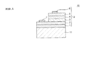
- FIG. 1 is a schematic sectional view of the LED wafer to be subjected to the reflective layer forming step.
- An LED wafer 10 includes a substrate 11 and a light emitting element 12.
- the substrate 11 is made of any appropriate material. Examples of the material for constituting the substrate 11 include sapphire, SiC, GaAs, GaN, and GaP. Note that, the substrate 11 is preferred to be ground (back-ground) to be thinned to any appropriate thickness.
- the thickness of the substrate 11 is preferably 10 ⁇ m to 500 ⁇ m, more preferably 50 ⁇ m to 300 ⁇ m, most preferably 80 ⁇ m to 150 ⁇ m.
- the light emitting element 12 includes a buffer layer 1, an n-type semiconductor layer 2, a light emitting layer 3, a p-type semiconductor layer 4, a transparent electrode 5, and electrodes 6 and 7.
- the light emitting layer 3 includes, for example, gallium nitride-based compounds (e.g., GaN, AlGaN, and InGaN), gallium phosphide-based compounds (e.g., GaP and GaAsP), gallium arsenide-based compounds (e.g., GaAs, AlGaAs, and AlGaInP), and zinc oxide (ZnO)-based compounds.
- gallium nitride-based compounds e.g., GaN, AlGaN, and InGaN
- gallium phosphide-based compounds e.g., GaP and GaAsP
- gallium arsenide-based compounds e.g., GaAs, AlGaAs, and AlGaInP
- ZnO zinc oxide
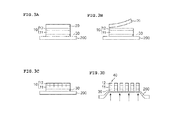
- FIGS. 2A to 2C are schematic views illustrating the reflective layer forming step in the method of manufacturing an LED according to the embodiment of the present invention.
- FIGS. 2A to 2C illustrate, as a representative example, an embodiment in which a reflective layer is formed on an outer side of the substrate of the LED wafer by a metal organic chemical vapor deposition method (MOCVD method).
- MOCVD method metal organic chemical vapor deposition method
- the LED wafer 10 having a heat-resistant pressure-sensitive adhesive sheet 20 attached thereto is subjected to the reflective layer forming step ( FIG. 2A ). At this time, the heat-resistant pressure-sensitive adhesive sheet 20 is attached onto the light emitting element 12 side of the LED wafer 10.
- any appropriate pressure-sensitive adhesive sheet may be used as long as the effect of the present invention may be obtained. It is preferred to use a heat-resistant pressure-sensitive adhesive sheet which does not melt and generate a gas and can maintain its adhesion even when the heat-resistant pressure-sensitive adhesive sheet is exposed under high temperature (for example, 135°C to 200°C) at the time of vapor deposition processing in the reflective layer forming step of the post-process.
- high temperature for example, 135°C to 200°C
- the heat-resistant pressure-sensitive adhesive sheet 20 includes, for example, a base member and a pressure-sensitive adhesive layer.
- the pressure-sensitive adhesive layer may be provided on one surface of the base member, or may be provided on each of both surfaces thereof.
- any appropriate material may be used as long as the effect of the present invention may be obtained.
- the material for constituting the base member include resins such as polyimide and polyethylene naphthalate. With use of such resins, a heat-resistant pressure-sensitive adhesive sheet excellent in heat-resisting performance can be obtained.
- the thickness of the base member is preferably 10 ⁇ m to 1,000 ⁇ m, more preferably 25 ⁇ m to 700 ⁇ m.
- the base member is a hard base member.
- the hard base member refers to a base member made of an inorganic material having a Young's modulus of 70 GPa or more at 25°C.
- the hard base member As a material for constituting the hard base member, there may be given, for example: silicon; glass; metal such as stainless steel; and a ceramic.
- the thickness of the hard base member is preferably 0.2 mm to 50 mm, more preferably 0.3 mm to 10 mm.
- any appropriate pressure-sensitive adhesive may be used. It is preferred to use a pressure-sensitive adhesive which does not melt and generate a gas and can maintain its adhesion even under high temperature (for example, 135°C to 200°C) at the time of vapor deposition. Further, the pressure-sensitive adhesive is preferred to be peeled off without adhesive residue even after heating. Examples of the pressure-sensitive adhesive include an acrylic pressure-sensitive adhesive, a silicone-based pressure-sensitive adhesive, and a polyimide-based pressure-sensitive adhesive.
- polyimide-based pressure-sensitive adhesives examples include a polyimide-based resin obtained by imidizing a polyamic acid obtained by a reaction of an acid anhydride and a diamine having an ester structure. It is preferred that the mixing ratio of the diamine having the ether structure when the acid anhydride is reacted with the diamine having the ether structure be 5 parts by weight to 90 parts by weight with respect to 100 parts by weight of the acid anhydride.
- a foaming agent may be added to the pressure-sensitive adhesive layer.
- the pressure-sensitive adhesive layer having the foaming agent added thereto exhibits a peel property by heating. Specifically, in the pressure-sensitive adhesive layer having the foaming agent added thereto, the foaming agent is foamed or expanded by heating, and thus the adhesion is reduced or lost.
- a heat-resistant pressure-sensitive adhesive sheet including such a pressure-sensitive adhesive layer can be adhered tightly to the LED wafer, and can be easily released when it is removed from LED wafer. With use of such a heat-resistant pressure-sensitive adhesive sheet, the damage to the LED wafer can be markedly prevented during releasing the heat-resistant pressure-sensitive adhesive sheet. Further, automated steps can be easily designed. Any appropriate foaming agent may be used as the foaming agent.
- foaming agent examples include: inorganic foaming agents such as ammonium carbonate, ammonium hydrogen carbonate, sodium hydrogen carbonate, ammonium nitrite, sodium boron hydride, and an azide; and organic foaming agents such as an alkane chloride fluoride, an azo-based compound, a hydrazine-based compound, a semicarbazide-based compound, a triazole-based compound, and an N-nitroso-based compound.
- inorganic foaming agents such as ammonium carbonate, ammonium hydrogen carbonate, sodium hydrogen carbonate, ammonium nitrite, sodium boron hydride, and an azide
- organic foaming agents such as an alkane chloride fluoride, an azo-based compound, a hydrazine-based compound, a semicarbazide-based compound, a triazole-based compound, and an N-nitroso-based compound.
- the thickness of the pressure-sensitive adhesive layer is preferably 1 ⁇ m to 100 ⁇ m, more preferably 3 ⁇ m to 60 ⁇ m.
- the LED wafer with the heat-resistant pressure-sensitive adhesive sheet is placed on a table 100 via the heat-resistant pressure-sensitive adhesive sheet 20, and a reflective layer 30 is formed on the outer side of the substrate 11 of the LED wafer 10 ( FIG. 2B ). At this time, the LED wafer 10 is placed with the light emitting element 12 side down. By forming the reflective layer 30, the amount of light to be extracted from the light emitting element 12 can be increased.
- any appropriate material may be used as long as the light from the light emitting element 12 may be satisfactorily reflected.
- the material for constituting the reflective layer 30 include metals such as aluminum, silver, gold, palladium, platinum, rhodium, and ruthenium.
- the reflective layer 30 made of a metal may be formed by, for example, a vapor deposition method (for example, as in the illustrated example, a MOCVD method). It is preferred that an underlayer made of, for example, SiO 2 , TiO 2 , ZrO 2 , and/or MgF 2 be formed on the outer side of the substrate 11 of the LED wafer 10, and then the reflective layer 30 made of a metal be formed by a vapor deposition method.
- the LED wafer 10 having the heat-resistant pressure-sensitive adhesive sheet 20 attached to the outer side of the light emitting element 12 is subjected to the reflective layer forming step. Therefore, the heat-resistant pressure-sensitive adhesive sheet 20 plays a role as a so-called masking sheet, and hence the metal may be prevented from entering behind the LED wafer 10 and depositing on the light emitting element 12. Further, as described above, when the hard base member is used as the base member of the heat-resistant pressure-sensitive adhesive sheet, the warpage of the LED wafer can be corrected, and hence it is possible to provide a manufacturing method having high reliability in terms of preventing the metal from depositing on the light emitting element 12. According to the manufacturing method of the present invention, a metal layer is hardly formed on the light emitting element 12, and hence an LED having high brightness can be obtained.
- the method of forming the reflective layer 30 is not limited to the MOCVD method, and any other appropriate methods may be employed.
- the other appropriate methods include an ion assisted electron beam deposition method.
- the ion assisted electron beam deposition method generally, the LED wafer is covered with a lid from a side opposite to the reflective layer forming side (that is, from the light emitting element side), and a reflective layer forming surface (that is, the outer surface of the substrate) is exposed. The exposed surface is subjected to vapor deposition processing.
- the metal may be prevented from entering behind the LED wafer and depositing on the light emitting element.
- the LED wafer 10 having the reflective layer 30 formed thereon can be obtained ( FIG. 2C ).
- the heat-resistant pressure-sensitive adhesive sheet 20 may be peeled off immediately after the reflective layer forming step, or the LED wafer 10 may be subjected to the post-process under a state in which the heat-resistant pressure-sensitive adhesive sheet 20 is still attached thereto.
- the LED wafer 10 can be prevented from being damaged during the post-process and during handling between steps.
- the method of manufacturing an LED of the present invention may further include any other appropriate steps.
- Examples of the other appropriate steps include a step of cutting the LED wafer 10 to singulate small element pieces (dicing step).
- FIGS. 3A to 3D are schematic views illustrating a dicing step in the method of manufacturing an LED according to the embodiment of the present invention.
- the LED wafer 10 that has undergone the reflective layer forming step is subjected to the dicing step.
- the LED wafer 10 is retained on dicing tape 200 with the reflective layer 30 side of the LED wafer 10 having the reflective layer 30 formed thereon down ( FIG. 3A ).
- the heat-resistant pressure-sensitive adhesive sheet 20 be peeled off after the LED wafer 10 is retained on the dicing tape 200 ( FIG.
- the LED wafer 10 (substantially, the substrate 11) is half-cut in the thickness direction ( FIG. 3C ).
- the dicing tape 200 is expanded so that the LED wafer 10 having the reflective layer 30 formed thereon is split from the cut portion as an origin to obtain LEDs 40 singulated into small element pieces ( FIG. 3D ).
- the LED wafer 10 is half-cut so as to split the LED wafer 10 from the cut portion as the origin (scribe dicing).
- the LED wafer 10 is half-cut from the light emitting element 12 side.
- the dicing tape 200 may be alternatively attached with the substrate 11 (reflective layer 30) side up, and the LED wafer 10 may be half-cut from the substrate 11 side (reflective layer 30 side).
- any appropriate method may be adopted as a method of cutting the LED wafer.
- Examples of other methods include a method of cutting the LED wafer in the entire thickness direction to singulate the small element pieces through expanding, and a method of laser cutting only the center portion of the LED wafer 10 in the thickness direction to split the LED wafer from the cut portion as an origin (stealth dicing).
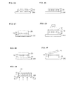
- FIGS. 4A to 4G are schematic views illustrating respective steps of a method of manufacturing an LED according to another embodiment of the present invention.
- the reflective layer 30 is formed after the cut portion for splitting is formed.
- the LED wafer 10 (for example, the LED wafer that has been subjected to a back-grinding step) is retained on dicing tape 200 ( FIG. 4A ), and then the LED wafer 10 is half-cut from the light emitting element 12 side ( FIG. 4B ).
- the heat-resistant pressure-sensitive adhesive sheet 20 is attached onto the outer side of the light emitting element 12 of the LED wafer 10 ( FIG. 4C ).
- the LED wafer 10 with the heat-resistant pressure-sensitive adhesive sheet is placed on the table 100 with the substrate 11 side up, and the reflective layer 30 is formed on the substrate 11 side of the LED wafer 10 ( FIG. 4D ).
- the LED wafer 10 with the heat-resistant pressure-sensitive adhesive sheet having the reflective layer 30 formed thereon is retained on the dicing tape 200 again with the side on which the cut portion is formed (heat-resistant pressure-sensitive adhesive sheet 20 side) up ( FIG. 4E ).
- the LED wafer 10 is split from the cut portion as an origin, to thereby obtain the LEDs 40 singulated into small element pieces ( FIG. 4G ).
- the LED wafer 10 is placed on the table via the heat-resistant pressure-sensitive adhesive sheet 20, and then the reflective layer 30 is formed on the LED wafer 10. After that, the LED wafer with the heat-resistant pressure-sensitive adhesive sheet is subjected to the post-process ( FIGS. 3A and 4E ). According to those embodiments, the heat-resistant pressure-sensitive adhesive sheet 20 protects the LED wafer 10, and thus the LED wafer 10 can be prevented from being damaged during handling.
Landscapes
- Led Devices (AREA)
Applications Claiming Priority (1)
| Application Number | Priority Date | Filing Date | Title |
|---|---|---|---|
| JP2012145450A JP2014011243A (ja) | 2012-06-28 | 2012-06-28 | Ledの製造方法 |
Publications (1)
| Publication Number | Publication Date |
|---|---|
| EP2680324A1 true EP2680324A1 (fr) | 2014-01-01 |
Family
ID=48577618
Family Applications (1)
| Application Number | Title | Priority Date | Filing Date |
|---|---|---|---|
| EP13171548.4A Withdrawn EP2680324A1 (fr) | 2012-06-28 | 2013-06-11 | Procédé de fabrication de DEL |
Country Status (6)
| Country | Link |
|---|---|
| US (1) | US20140004635A1 (fr) |
| EP (1) | EP2680324A1 (fr) |
| JP (1) | JP2014011243A (fr) |
| KR (1) | KR20140001781A (fr) |
| CN (1) | CN103531675A (fr) |
| TW (1) | TW201403889A (fr) |
Families Citing this family (1)
| Publication number | Priority date | Publication date | Assignee | Title |
|---|---|---|---|---|
| DE102014117591A1 (de) * | 2014-12-01 | 2016-06-02 | Osram Opto Semiconductors Gmbh | Halbleiterchip, Verfahren zur Herstellung einer Vielzahl an Halbleiterchips und Verfahren zur Herstellung eines elektronischen oder optoelektronischen Bauelements und elektronisches oder optoelektronisches Bauelement |
Citations (14)
| Publication number | Priority date | Publication date | Assignee | Title |
|---|---|---|---|---|
| JPS6333487A (ja) | 1987-04-17 | 1988-02-13 | Nitto Electric Ind Co Ltd | 発泡型粘着シ−ト |
| JPH02305878A (ja) | 1989-05-19 | 1990-12-19 | Nitto Denko Corp | 膨脹型粘着部材 |
| GB2242783A (en) * | 1990-04-06 | 1991-10-09 | Telefunken Electronic Gmbh | Light emitting semiconductor device |
| JPH0543851A (ja) | 1991-08-14 | 1993-02-23 | Nitto Denko Corp | 剥離性感圧接着剤及びその粘着部材 |
| JP2001085746A (ja) | 1999-09-14 | 2001-03-30 | Seiwa Electric Mfg Co Ltd | Ledチップ |
| JP2002083785A (ja) * | 2000-09-07 | 2002-03-22 | Nec Kansai Ltd | 半導体素子の製造方法 |
| US6398892B1 (en) * | 1998-08-26 | 2002-06-04 | Lintec Corporation | Method of using pressure sensitive adhesive double coated sheet |
| JP2003273042A (ja) * | 2002-03-13 | 2003-09-26 | Lintec Corp | 半導体装置の製造方法 |
| US20050104081A1 (en) * | 2003-11-18 | 2005-05-19 | Kim Seong-Jin | Semiconductor light emitting diode and method for manufacturing the same |
| US20060289892A1 (en) * | 2005-06-27 | 2006-12-28 | Lee Jae S | Method for preparing light emitting diode device having heat dissipation rate enhancement |
| EP1753018A2 (fr) * | 2005-08-12 | 2007-02-14 | Samsung Electro-Mechanics Co., Ltd. | Procédé pour fabriquer un substrat monocristallin à base de nitrure et procédé de fabrication d'un dispositif semiconducteur à base de nitrure |
| EP1883106A2 (fr) * | 2006-07-13 | 2008-01-30 | Nitto Denko Corporation | Procédé pour travailler un objet |
| US20090078952A1 (en) * | 2007-09-21 | 2009-03-26 | Ray-Hua Horng | Light-emitting chip device with high thermal conductivity |
| US7998768B1 (en) * | 2010-10-13 | 2011-08-16 | Ray-Hua Horng | Method for forming a light emitting diode |
Family Cites Families (2)
| Publication number | Priority date | Publication date | Assignee | Title |
|---|---|---|---|---|
| US20040000672A1 (en) * | 2002-06-28 | 2004-01-01 | Kopin Corporation | High-power light-emitting diode structures |
| JP2008060151A (ja) * | 2006-08-29 | 2008-03-13 | Nitto Denko Corp | 半導体ウエハ裏面加工方法、基板裏面加工方法、及び放射線硬化型粘着シート |
-
2012
- 2012-06-28 JP JP2012145450A patent/JP2014011243A/ja active Pending
-
2013
- 2013-06-11 EP EP13171548.4A patent/EP2680324A1/fr not_active Withdrawn
- 2013-06-12 US US13/915,988 patent/US20140004635A1/en not_active Abandoned
- 2013-06-19 TW TW102121806A patent/TW201403889A/zh unknown
- 2013-06-27 KR KR1020130074521A patent/KR20140001781A/ko not_active Withdrawn
- 2013-06-28 CN CN201310269366.4A patent/CN103531675A/zh active Pending
Patent Citations (14)
| Publication number | Priority date | Publication date | Assignee | Title |
|---|---|---|---|---|
| JPS6333487A (ja) | 1987-04-17 | 1988-02-13 | Nitto Electric Ind Co Ltd | 発泡型粘着シ−ト |
| JPH02305878A (ja) | 1989-05-19 | 1990-12-19 | Nitto Denko Corp | 膨脹型粘着部材 |
| GB2242783A (en) * | 1990-04-06 | 1991-10-09 | Telefunken Electronic Gmbh | Light emitting semiconductor device |
| JPH0543851A (ja) | 1991-08-14 | 1993-02-23 | Nitto Denko Corp | 剥離性感圧接着剤及びその粘着部材 |
| US6398892B1 (en) * | 1998-08-26 | 2002-06-04 | Lintec Corporation | Method of using pressure sensitive adhesive double coated sheet |
| JP2001085746A (ja) | 1999-09-14 | 2001-03-30 | Seiwa Electric Mfg Co Ltd | Ledチップ |
| JP2002083785A (ja) * | 2000-09-07 | 2002-03-22 | Nec Kansai Ltd | 半導体素子の製造方法 |
| JP2003273042A (ja) * | 2002-03-13 | 2003-09-26 | Lintec Corp | 半導体装置の製造方法 |
| US20050104081A1 (en) * | 2003-11-18 | 2005-05-19 | Kim Seong-Jin | Semiconductor light emitting diode and method for manufacturing the same |
| US20060289892A1 (en) * | 2005-06-27 | 2006-12-28 | Lee Jae S | Method for preparing light emitting diode device having heat dissipation rate enhancement |
| EP1753018A2 (fr) * | 2005-08-12 | 2007-02-14 | Samsung Electro-Mechanics Co., Ltd. | Procédé pour fabriquer un substrat monocristallin à base de nitrure et procédé de fabrication d'un dispositif semiconducteur à base de nitrure |
| EP1883106A2 (fr) * | 2006-07-13 | 2008-01-30 | Nitto Denko Corporation | Procédé pour travailler un objet |
| US20090078952A1 (en) * | 2007-09-21 | 2009-03-26 | Ray-Hua Horng | Light-emitting chip device with high thermal conductivity |
| US7998768B1 (en) * | 2010-10-13 | 2011-08-16 | Ray-Hua Horng | Method for forming a light emitting diode |
Also Published As
| Publication number | Publication date |
|---|---|
| US20140004635A1 (en) | 2014-01-02 |
| CN103531675A (zh) | 2014-01-22 |
| TW201403889A (zh) | 2014-01-16 |
| JP2014011243A (ja) | 2014-01-20 |
| KR20140001781A (ko) | 2014-01-07 |
Similar Documents
| Publication | Publication Date | Title |
|---|---|---|
| TWI726494B (zh) | 分離形成於基板晶圓上之發光裝置之方法 | |
| JP5073917B2 (ja) | 電気的なコンタクトを有する光電子半導体チップならびに該光電子半導体チップを製造するための方法 | |
| TW567616B (en) | Production method for a radiation-emitting semiconductor-element | |
| CN103430330B (zh) | 用于制造至少一个光电子半导体芯片的方法 | |
| US20140000793A1 (en) | Method of manufacturing an led | |
| US20140120699A1 (en) | Fabrication method for dicing of semiconductor wafers using laser cutting techniques | |
| US20070194296A1 (en) | Light emitting diode and manufacturing method therefor | |
| US20050263854A1 (en) | Thick laser-scribed GaN-on-sapphire optoelectronic devices | |
| EP1753018B1 (fr) | Procédé pour fabriquer un substrat monocristallin à base de nitrure et procédé de fabrication d'un dispositif semiconducteur à base de nitrure | |
| US7892873B2 (en) | Fabrication method of nitride-based semiconductor device | |
| JP2008306021A (ja) | Ledチップの製造方法 | |
| JP2013504197A (ja) | 湾曲を制御する層を備えたiii族の窒化物の発光デバイス | |
| EP2680325A2 (fr) | Procédé de fabrication de diode électroluminescente | |
| US10249806B2 (en) | Solid state optoelectronic device with preformed metal support substrate | |
| US20120100695A1 (en) | Manufacturing method of semiconductor device | |
| TWI535057B (zh) | 具有側反射性之固態照明裝置及其相關製造方法 | |
| EP2367209A2 (fr) | Procédé de fabrication de dispositif électroluminescent semi-conducteur | |
| US20140004635A1 (en) | Method of manufacturing an led | |
| EP2680322A1 (fr) | Procédé de fabrication de DEL | |
| JP5596375B2 (ja) | 半導体発光素子の製造方法及び半導体発光素子 | |
| WO2008065929A1 (fr) | Procédé de production d'élément d'émission de lumière | |
| KR101459809B1 (ko) | 발광 소자 | |
| JP2005039000A (ja) | 半導体発光素子およびその製造方法 | |
| JP2005197286A (ja) | 半導体薄膜のハンドリング方法および発光素子の製造方法 |
Legal Events
| Date | Code | Title | Description |
|---|---|---|---|
| PUAI | Public reference made under article 153(3) epc to a published international application that has entered the european phase |
Free format text: ORIGINAL CODE: 0009012 |
|
| AK | Designated contracting states |
Kind code of ref document: A1 Designated state(s): AL AT BE BG CH CY CZ DE DK EE ES FI FR GB GR HR HU IE IS IT LI LT LU LV MC MK MT NL NO PL PT RO RS SE SI SK SM TR |
|
| AX | Request for extension of the european patent |
Extension state: BA ME |
|
| STAA | Information on the status of an ep patent application or granted ep patent |
Free format text: STATUS: THE APPLICATION IS DEEMED TO BE WITHDRAWN |
|
| 18D | Application deemed to be withdrawn |
Effective date: 20140702 |