EP2681765B1 - Appareils et procédé liés à la réduction des pertes de signaux RF - Google Patents
Appareils et procédé liés à la réduction des pertes de signaux RF Download PDFInfo
- Publication number
- EP2681765B1 EP2681765B1 EP12752146.6A EP12752146A EP2681765B1 EP 2681765 B1 EP2681765 B1 EP 2681765B1 EP 12752146 A EP12752146 A EP 12752146A EP 2681765 B1 EP2681765 B1 EP 2681765B1
- Authority
- EP
- European Patent Office
- Prior art keywords
- electronic circuit
- bonding pad
- output
- lead
- circuit module
- Prior art date
- Legal status (The legal status is an assumption and is not a legal conclusion. Google has not performed a legal analysis and makes no representation as to the accuracy of the status listed.)
- Active
Links
Images


Classifications
-
- H—ELECTRICITY
- H10—SEMICONDUCTOR DEVICES; ELECTRIC SOLID-STATE DEVICES NOT OTHERWISE PROVIDED FOR
- H10W—GENERIC PACKAGES, INTERCONNECTIONS, CONNECTORS OR OTHER CONSTRUCTIONAL DETAILS OF DEVICES COVERED BY CLASS H10
- H10W44/00—Electrical arrangements for controlling or matching impedance
- H10W44/20—Electrical arrangements for controlling or matching impedance at high-frequency [HF] or radio frequency [RF]
-
- H—ELECTRICITY
- H10—SEMICONDUCTOR DEVICES; ELECTRIC SOLID-STATE DEVICES NOT OTHERWISE PROVIDED FOR
- H10W—GENERIC PACKAGES, INTERCONNECTIONS, CONNECTORS OR OTHER CONSTRUCTIONAL DETAILS OF DEVICES COVERED BY CLASS H10
- H10W72/00—Interconnections or connectors in packages
-
- H—ELECTRICITY
- H10—SEMICONDUCTOR DEVICES; ELECTRIC SOLID-STATE DEVICES NOT OTHERWISE PROVIDED FOR
- H10W—GENERIC PACKAGES, INTERCONNECTIONS, CONNECTORS OR OTHER CONSTRUCTIONAL DETAILS OF DEVICES COVERED BY CLASS H10
- H10W44/00—Electrical arrangements for controlling or matching impedance
- H10W44/20—Electrical arrangements for controlling or matching impedance at high-frequency [HF] or radio frequency [RF]
- H10W44/203—Electrical connections
- H10W44/206—Wires
-
- H—ELECTRICITY
- H10—SEMICONDUCTOR DEVICES; ELECTRIC SOLID-STATE DEVICES NOT OTHERWISE PROVIDED FOR
- H10W—GENERIC PACKAGES, INTERCONNECTIONS, CONNECTORS OR OTHER CONSTRUCTIONAL DETAILS OF DEVICES COVERED BY CLASS H10
- H10W44/00—Electrical arrangements for controlling or matching impedance
- H10W44/20—Electrical arrangements for controlling or matching impedance at high-frequency [HF] or radio frequency [RF]
- H10W44/241—Electrical arrangements for controlling or matching impedance at high-frequency [HF] or radio frequency [RF] for passive devices or passive elements
-
- H—ELECTRICITY
- H10—SEMICONDUCTOR DEVICES; ELECTRIC SOLID-STATE DEVICES NOT OTHERWISE PROVIDED FOR
- H10W—GENERIC PACKAGES, INTERCONNECTIONS, CONNECTORS OR OTHER CONSTRUCTIONAL DETAILS OF DEVICES COVERED BY CLASS H10
- H10W70/00—Package substrates; Interposers; Redistribution layers [RDL]
- H10W70/60—Insulating or insulated package substrates; Interposers; Redistribution layers
- H10W70/62—Insulating or insulated package substrates; Interposers; Redistribution layers characterised by their interconnections
- H10W70/65—Shapes or dispositions of interconnections
-
- H—ELECTRICITY
- H10—SEMICONDUCTOR DEVICES; ELECTRIC SOLID-STATE DEVICES NOT OTHERWISE PROVIDED FOR
- H10W—GENERIC PACKAGES, INTERCONNECTIONS, CONNECTORS OR OTHER CONSTRUCTIONAL DETAILS OF DEVICES COVERED BY CLASS H10
- H10W72/00—Interconnections or connectors in packages
- H10W72/071—Connecting or disconnecting
- H10W72/075—Connecting or disconnecting of bond wires
-
- H—ELECTRICITY
- H10—SEMICONDUCTOR DEVICES; ELECTRIC SOLID-STATE DEVICES NOT OTHERWISE PROVIDED FOR
- H10W—GENERIC PACKAGES, INTERCONNECTIONS, CONNECTORS OR OTHER CONSTRUCTIONAL DETAILS OF DEVICES COVERED BY CLASS H10
- H10W72/00—Interconnections or connectors in packages
- H10W72/50—Bond wires
- H10W72/541—Dispositions of bond wires
- H10W72/547—Dispositions of multiple bond wires
- H10W72/5475—Dispositions of multiple bond wires multiple bond wires connected to common bond pads at both ends of the wires
-
- H—ELECTRICITY
- H10—SEMICONDUCTOR DEVICES; ELECTRIC SOLID-STATE DEVICES NOT OTHERWISE PROVIDED FOR
- H10W—GENERIC PACKAGES, INTERCONNECTIONS, CONNECTORS OR OTHER CONSTRUCTIONAL DETAILS OF DEVICES COVERED BY CLASS H10
- H10W72/00—Interconnections or connectors in packages
- H10W72/50—Bond wires
- H10W72/551—Materials of bond wires
- H10W72/552—Materials of bond wires comprising metals or metalloids, e.g. silver
- H10W72/5522—Materials of bond wires comprising metals or metalloids, e.g. silver comprising gold [Au]
-
- H—ELECTRICITY
- H10—SEMICONDUCTOR DEVICES; ELECTRIC SOLID-STATE DEVICES NOT OTHERWISE PROVIDED FOR
- H10W—GENERIC PACKAGES, INTERCONNECTIONS, CONNECTORS OR OTHER CONSTRUCTIONAL DETAILS OF DEVICES COVERED BY CLASS H10
- H10W72/00—Interconnections or connectors in packages
- H10W72/50—Bond wires
- H10W72/59—Bond pads specially adapted therefor
-
- H—ELECTRICITY
- H10—SEMICONDUCTOR DEVICES; ELECTRIC SOLID-STATE DEVICES NOT OTHERWISE PROVIDED FOR
- H10W—GENERIC PACKAGES, INTERCONNECTIONS, CONNECTORS OR OTHER CONSTRUCTIONAL DETAILS OF DEVICES COVERED BY CLASS H10
- H10W72/00—Interconnections or connectors in packages
- H10W72/90—Bond pads, in general
- H10W72/951—Materials of bond pads
- H10W72/952—Materials of bond pads comprising metals or metalloids, e.g. PbSn, Ag or Cu
-
- H—ELECTRICITY
- H10—SEMICONDUCTOR DEVICES; ELECTRIC SOLID-STATE DEVICES NOT OTHERWISE PROVIDED FOR
- H10W—GENERIC PACKAGES, INTERCONNECTIONS, CONNECTORS OR OTHER CONSTRUCTIONAL DETAILS OF DEVICES COVERED BY CLASS H10
- H10W90/00—Package configurations
- H10W90/701—Package configurations characterised by the relative positions of pads or connectors relative to package parts
- H10W90/751—Package configurations characterised by the relative positions of pads or connectors relative to package parts of bond wires
- H10W90/754—Package configurations characterised by the relative positions of pads or connectors relative to package parts of bond wires between a chip and a stacked insulating package substrate, interposer or RDL
Definitions
- the present disclosure generally relates to the field of integrated circuit layout and packaging, and more particularly to systems and methods of layout and forming wire bond pads for packaging of Radio Frequency (RF) integrated circuits (ICs).
- RF Radio Frequency
- Silicon or other semiconductor wafers are fabricated into integrated circuits (ICs) as is known to one of ordinary skill in the art of IC fabrication.
- An IC is bonded and electrically connected to a carrier or substrate, which has layers of dielectric and metal traces, and packaged for use.
- a surface plating material is plated onto the top layer of copper traces to provide electrical connection points between the IC and the substrate, permitting the IC to interface with the outside world.
- Ni/Au nickel/gold
- the RFIC is wire-bonded to the Ni/Au wire-bond pads plated on the surface of the substrate to form the electrical connections of the RFIC with its package.
- increases in gold prices have increased packaging costs associated with the Ni/Au surface plating.
- US patent application with publication number US 2008/206927 discloses an external component, typically a surface mounted passive component, attached to a semiconductor die.
- the passive component may be placed directly over exposed pads on the semiconductor die and attached using conductive tape or conductive epoxy; or the passive component may be attached to the semiconductor die using non-conductive adhesive and wire bonded to bond pads on the semiconductor die and/or to pads on a substrate to which the semiconductor die is attached.
- Japanese patent application with publication number JP2005093545 discloses a semiconductor circuit device in which a bonding pad is arranged at a former side of an intersecting portion of a signal course, and one side's wiring is carried out overhead by a bonding wire so that wiring of a signal source is made not so long, and parasitic capacitance at the intersecting portion is reduced.
- a capacitor which carries out series resonance with inductance of the bonding wire or a terminal at a specific frequency is inserted in the former side of a GND, thereby forming a trap with respect to the frequency.
- the module comprises an electronic circuit device having an output signal and a current associated therewith.
- Said electronic circuit device includes a first lead, a second lead, and an integrated circuit die having an on-die passive component.
- the electronic circuit module further comprises a substrate including a trace for conducting said current.
- Said trace has a first bonding pad thereon electrically connected to said first lead and a second bonding pad located on the trace between the first bonding pad and the output of the electronic circuit module and being electrically connected to said second lead.
- Said electronic circuit device is configured such that said on-die passive component electrically connects to said first lead and said output signal electrically connects to said second lead. Said current thereby being directed away from said first bonding pad.
- the electronic circuit module is a radio frequency integrated circuit module and the signal losses are radio frequency signal losses.
- the electronic circuit device is a radio frequency electronic circuit device, the output signal is a radio frequency output signal, and the current is a radio frequency current.
- a method for fabricating an electronic circuit module for reducing signal losses in the electronic circuit module comprises fabricating an electronic circuit device including an integrated circuit die having an on-die passive component, and configured for generating an output signal from the electronic circuit device. Said output signal has an associated current.
- the method further comprises forming a first lead and a second lead on the electronic circuit device, forming a first bonding pad and a second bonding pad on a substrate, and forming a trace on the substrate to provide a conductive path to conduct the current between the first and the second bonding pads and from the said output to an output of the electronic circuit module.
- the method further comprises electrically connecting the first lead to the first bonding pad, electrically connecting the second lead to the second bonding pad, the first bonding pad being located on the trace, the second bonding pad being located on the trace between the first bonding pad and the output of the electronic circuit module, and configuring the electronic circuit device so that the on-die passive component electrically connects to the first lead and the output signal electrically connects to the second lead.
- the current thereby being directed away from the first bonding pad.
- the electronic circuit device is a radio frequency electronic circuit device, the output signal is a radio frequency output signal, and the current is a radio frequency current.
- Wire bonding is a technique for connecting electrical circuit devices, for example, integrated circuit (IC) die, to the next level of packaging.
- These circuit devices generally comprise a plurality of small conductive leads/pads that are electrically connected, for example, by ball bonding, wedge bonding, or the like, to wire bond pads on conductors embedded in the device package or substrate.
- the wire bond pads on the substrate provide the electrical connections between the IC and the substrate, permitting the IC to interface with the outside world.
- the wire is attached at both ends using some combination of heat, pressure, and ultrasonic energy to make a weld.
- a plurality of copper patterns is formed on a substrate which is electrically connected to the circuit patterns, and a filler, such as a dielectric, is filled between the copper patterns such that an upper surface of the copper pattern is exposed.
- bare copper is not readily solderable or bondable and requires plating with a material that facilitates soldering or bonding. Areas that should not be solderable/bondable are covered with a material to resist plating.
- solder resist refers to a polymer coating that acts as a mask and prevents the plating material from adhering to the masked copper traces.
- a surface plating material is plated onto the top layer of exposed copper traces to provide the wire bond pads.
- wire bond pads are suited for wire bonding directly over active circuits to avoid damaging fragile devices and to lower metal resistance for power integrated circuits.
- FIGURE 1 illustrates a portion of an IC module 100 comprising an IC 102, a substrate 116, a copper trace 104, wire bond pads 106a, 106b, and bonding wires 108, according to an embodiment.
- the IC is wire bonded to wire bond pads 106 through wires 108.
- wire bond pad 106a is a 6-wire wire bond pad and wire bond pad 106b is a 3-wire wire bond pad. In other embodiment, other numbers of wires 108 can be attached to the wire-bond pads 106.
- Wire bond pad 106 comprises a bond area 114, sidewalls 110, and edges 112.
- Wafer fabrication generally refers to the process of building integrated circuits on silicon or semiconductor wafers.
- Many processes exist known to one of ordinary skill in the art of wafer fabrication, such as, for example, epitaxy, masking and etching, diffusion, ion implant, deposition of polysilicon, dielectric fabrication, lithography/etching, deposition of thin films, metallization, glassivation, probing/trimming of each die on the wafer, and the like, to create integrated circuits to the designers specifications.
- an on-die passive device such as a resistor, capacitor, inductor, or the like
- the on-die passive device can function as a filter, a shunt filter, a trapper for harmonic frequencies, or the like, in the RF circuit.
- FIGURE 9 illustrates an enlarged portion of an RFIC module 800 not falling within the scope of the present invention comprising a substrate 810 and an RFIC 818. Additional circuitry is omitted for simplicity.
- the substrate 810 comprises an RFIC circuit trace 812, and wire-bonding pads 814a, 814b.
- the wire-bonding pads 814a, 814b comprise Ni/Pd/Au.
- the wire-bonding pads 814a, 814b comprise a high RF loss plating material.
- the wire bonding pads 814a, 814b comprise Ni/Au.
- the wire bonding pads 814a, 814b are formed with plated edges and sidewalls, as illustrated in FIGURE 9 .
- the wire bonding pads 814a, 814b are formed with edges and sidewalls free from the surface plating material.
- the RFIC 818 comprises an RF output 820, and an on-die passive device 822, such as a capacitor 822.
- the RF output 820 is the location on the RFIC 818 from which the RF output signal from the RFIC's internal circuitry exits the RFIC 818 and inputs into the RF circuitry of the module 800.
- the layout of the RFIC 818 is configured such that the capacitor 822 is placed in the RF circuit 812 of the RF module 800 after the RF output 820.
- the on-die capacitor 822 is between the RF output 820 of the RFIC 818 and the RF output of the module 800.
- An arrow 816 indicates the direction of RF current flow of the RF signal.
- the RF current flows from the RF output signal 820 to the RF output of the module 800.
- Portions of the RF trace 812 that are between the RF output signal 820 and the RF output of the module 800 are in the RF signal down path and portions of the trace 812 that are located above the RF output 820 that do not receive the RF current flow are in the RF signal upper path.
- the capacitor bonding pad 814b is located in the RF down path. In other words, the RF current passes through the capacitor wire-bond pad 814b when traveling from the RF output 820 to the rest of the circuitry on the substrate 810.
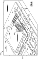
- FIGURE 10 illustrates the enlarged portion of an RFIC module 900 comprising a substrate 910 and an RFIC 918 according to the present invention.
- the substrate 910 comprises an RFIC circuit trace 912, and wire-bonding pads 914a, 914b.
- the wire-bonding pads 914a, 914b comprise Ni/Pd/Au.
- the wire-bonding pads 914a, 914b comprise a high RF loss plating material.
- the wire bonding pads 914a, 914b comprise Ni/Au.
- the wire bonding pads 914a, 914b are formed with plated edges and sidewalls, as illustrated in FIGURE 10 .
- the wire bonding pads 914a, 914b are formed with edges and sidewalls free from the surface plating material.
- the layout of the RFIC 918 has been reconfigured to reduce the RF losses associated with the RF current flowing through the high RF loss bonding pad of the on-die passive device.
- the RFIC 918 comprises an RF output 920, and an on-die passive device 922, such as a capacitor 922.
- the RF output 920 is the location on the RFIC 918 from which the RF output signal from the RFIC's internal circuitry exits the RFIC 918 and inputs into the RF circuitry of the module 900.
- the layout of the RFIC 918 is configured such that the capacitor 922 is placed in the RF circuit 912 of the RF module 900 before the RF output 920.
- the on-die capacitor 922 is not between the RF output 920 of the RFIC 918 and the RF output of the module 900.
- the arrow 816 again indicates the direction of RF current flow of the RF signal.
- the RF current flows from the RF output signal 920 to the RF output of the module 900.
- the passive device bonding pad 914a is located in the RF upper path. In other words, the RF current does not pass through the passive device wire-bond pad 914a when traveling from the RF output 920 to the rest of the circuitry on the substrate 910.
- placing the on-die passive device in the layout of the RFIC 918 such that bonding pad 914a on the substrate 910 for the on-die passive device is in the RF upper signal path reduces the RF signal loss that is associated with placing the on-die passive device bonding pad 914a in the RF signal down path.
- Ni/Pd/Au instead of Ni/Au is plated onto the surface traces of substrates for RFIC modules to form wire-bond areas.
- Ni/Pd/Au has a higher RF sheet resistance than Ni/Au and this leads to higher RF losses for signals traveling through Ni/Pd/Au wire-bond areas than for signals traveling through Ni/Au wire-bond areas.
- an on-die passive device such as a capacitor, resistor, inductor, or the like, associated with an RFIC is placed in an RF upper path with respect to the RFIC output signal. By laying out the IC with the passive device in the RF signal upper path, the RF signal current does not pass through the high RF loss bonding pad of the passive device when module is assembled.
- Ni/Pd/Au surface plating While examples have been described with respect to Ni/Pd/Au surface plating, the disclosed systems and methods apply to any high RF loss surface plating, such as, for example, Sn, Pb, other surfaces of ferromagnetic materials, and the like.
Landscapes
- Wire Bonding (AREA)
- Semiconductor Integrated Circuits (AREA)
Claims (5)
- Module de circuit électronique (900) configuré pour réduire les pertes de signal, ledit module comprenant :un dispositif de circuit électronique (918) comportant : une puce de circuit intégré présentant un composant passif sur puce (922), une sortie (920) configurée pour fournir un signal de sortie ayant un courant associé au module de circuit électronique (900), une première broche de raccordement et une seconde broche de raccordement ;un substrat (910) comprenant une piste (912) pour conduire le courant depuis ladite sortie (920) jusqu'à une sortie du module de circuit électronique, la piste comportant sur celle-ci un premier plot de connexion (914a) connecté électriquement à la première broche de raccordement et un second plot de connexion (914b) situé sur la piste (912) entre le premier plot de connexion (91 4a) et la sortie du module de circuit électronique et étant connecté électriquement à la seconde broche de raccordement, ledit dispositif de circuit électronique étant configuré de telle sorte que ledit composant passif sur puce (922) se connecte électriquement à ladite première broche de raccordement et que le signal de ladite sortie (920) se connecte électriquement à la seconde broche de raccordement, le courant étant ainsi dirigé loin du premier plot de connexion, le dispositif électronique étant un dispositif de circuit électronique radiofréquence, le signal de sortie étant un signal de sortie radiofréquence, et le courant étant un courant de radiofréquence.
- Module de circuit électronique selon la revendication 1 dans lequel les premier et second plots de connexion (914a, 914b) sont plaqués avec un matériau de placage en surface comprenant du nickel, du palladium et de l'or.
- Module de circuit électronique selon la revendication 1 ou la revendication 2 dans lequel le premier plot de connexion (914a) et le second plot de connexion (914b) comportent chacun au moins un bord, au moins un flanc et une zone de connexion, l'au moins un bord et l'au moins un flanc de chacun des premier et second plots de connexion (914a, 91 4b) étant dépourvus de matériau de placage.
- Module de circuit électronique selon l'une quelconque des revendications 1 à 3 dans lequel le premier plot de connexion (914a) et le second plot de connexion (914b) sont des plots de connexion filaire.
- Procédé de fabrication d'un module de circuit électronique (900) pour réduire les pertes de signal dans le module de circuit électronique, le procédé comprenant :la fabrication d'un dispositif de circuit électronique (918) comprenant : une puce de circuit intégré présentant un composant passif sur puce (922) et une sortie (920) configurée pour fournir un signal de sortie ayant un courant associé au module de circuit électronique (900), le module de circuit électronique comprenant le dispositif de circuit électronique ;la formation d'une première broche de raccordement et d'une seconde broche de raccordement sur le dispositif de circuit électronique ;la formation d'un premier plot de connexion (914a) et d'un second plot de connexion (914b) sur un substrat (910), le module de circuit électronique comprenant le substrat (910) ;la formation d'une piste (912) sur le substrat (910) pour fournir un chemin conducteur afin de conduire le courant entre les premier et second plots de connexion (914a, 914b) et depuis ladite sortie (920) jusqu'à une sortie du module de circuit électronique ;la connexion électrique de la première broche de raccordement au premier plot de connexion (914a) ;la connexion électrique de la seconde broche de raccordement au second plot de connexion (914b), le premier plot de connexion étant situé sur la piste, le second plot de connexion étant situé sur la piste (912) entre le premier plot de connexion (914a) et la sortie du module de circuit électronique ; etla configuration du dispositif de circuit électronique de telle sorte que le composant passif sur puce (922) se connecte électriquement à la première broche de raccordement et que le signal de sortie se connecte électriquement à la seconde broche de raccordement, le courant étant ainsi dirigé loin du premier plot de connexion pendant l'utilisation, le dispositif de circuit électronique étant un dispositif de circuit électronique radiofréquence, le signal de sortie étant un signal de sortie radiofréquence, et le courant étant un courant de radiofréquence.
Applications Claiming Priority (3)
| Application Number | Priority Date | Filing Date | Title |
|---|---|---|---|
| US13/040,137 US8686537B2 (en) | 2011-03-03 | 2011-03-03 | Apparatus and methods for reducing impact of high RF loss plating |
| US13/040,127 US8889995B2 (en) | 2011-03-03 | 2011-03-03 | Wire bond pad system and method |
| PCT/US2012/027130 WO2012118896A2 (fr) | 2011-03-03 | 2012-02-29 | Appareil et procédés liés aux plots de connexion de fils et permettant de réduire l'impact du revêtement métallique à pertes rf élevées |
Publications (3)
| Publication Number | Publication Date |
|---|---|
| EP2681765A2 EP2681765A2 (fr) | 2014-01-08 |
| EP2681765A4 EP2681765A4 (fr) | 2015-04-22 |
| EP2681765B1 true EP2681765B1 (fr) | 2022-04-06 |
Family
ID=46758476
Family Applications (1)
| Application Number | Title | Priority Date | Filing Date |
|---|---|---|---|
| EP12752146.6A Active EP2681765B1 (fr) | 2011-03-03 | 2012-02-29 | Appareils et procédé liés à la réduction des pertes de signaux RF |
Country Status (4)
| Country | Link |
|---|---|
| EP (1) | EP2681765B1 (fr) |
| KR (1) | KR101776364B1 (fr) |
| CN (1) | CN103503133B (fr) |
| WO (1) | WO2012118896A2 (fr) |
Families Citing this family (3)
| Publication number | Priority date | Publication date | Assignee | Title |
|---|---|---|---|---|
| US9679869B2 (en) | 2011-09-02 | 2017-06-13 | Skyworks Solutions, Inc. | Transmission line for high performance radio frequency applications |
| KR102250612B1 (ko) | 2012-06-14 | 2021-05-10 | 스카이워크스 솔루션즈, 인코포레이티드 | 고조파 종단 회로를 포함하는 전력 증폭기 모듈 및 관련된 시스템, 장치, 및 방법 |
| CN109065517B (zh) * | 2014-09-23 | 2020-12-01 | 华为技术有限公司 | 射频功率组件及射频信号收发设备 |
Citations (2)
| Publication number | Priority date | Publication date | Assignee | Title |
|---|---|---|---|---|
| US6759597B1 (en) * | 1998-02-02 | 2004-07-06 | International Business Machines Corporation | Wire bonding to dual metal covered pad surfaces |
| JP2005093545A (ja) * | 2003-09-12 | 2005-04-07 | Matsushita Electric Ind Co Ltd | 半導体回路装置 |
Family Cites Families (10)
| Publication number | Priority date | Publication date | Assignee | Title |
|---|---|---|---|---|
| US6534192B1 (en) * | 1999-09-24 | 2003-03-18 | Lucent Technologies Inc. | Multi-purpose finish for printed wiring boards and method of manufacture of such boards |
| US20070176287A1 (en) | 1999-11-05 | 2007-08-02 | Crowley Sean T | Thin integrated circuit device packages for improved radio frequency performance |
| US6294966B1 (en) * | 1999-12-31 | 2001-09-25 | Hei, Inc. | Interconnection device |
| US6621140B1 (en) * | 2002-02-25 | 2003-09-16 | Rf Micro Devices, Inc. | Leadframe inductors |
| CN2570979Y (zh) * | 2002-09-19 | 2003-09-03 | 威盛电子股份有限公司 | 芯片封装结构 |
| US8310060B1 (en) * | 2006-04-28 | 2012-11-13 | Utac Thai Limited | Lead frame land grid array |
| US7867806B2 (en) * | 2007-02-26 | 2011-01-11 | Flextronics Ap, Llc | Electronic component structure and method of making |
| US8299572B2 (en) * | 2007-06-20 | 2012-10-30 | Skyworks Solutions, Inc | Semiconductor die with backside passive device integration |
| US7618846B1 (en) * | 2008-06-16 | 2009-11-17 | Stats Chippac, Ltd. | Semiconductor device and method of forming shielding along a profile disposed in peripheral region around the device |
| US8378485B2 (en) * | 2009-07-13 | 2013-02-19 | Lsi Corporation | Solder interconnect by addition of copper |
-
2012
- 2012-02-29 WO PCT/US2012/027130 patent/WO2012118896A2/fr not_active Ceased
- 2012-02-29 KR KR1020137025979A patent/KR101776364B1/ko active Active
- 2012-02-29 CN CN201280021283.7A patent/CN103503133B/zh active Active
- 2012-02-29 EP EP12752146.6A patent/EP2681765B1/fr active Active
Patent Citations (2)
| Publication number | Priority date | Publication date | Assignee | Title |
|---|---|---|---|---|
| US6759597B1 (en) * | 1998-02-02 | 2004-07-06 | International Business Machines Corporation | Wire bonding to dual metal covered pad surfaces |
| JP2005093545A (ja) * | 2003-09-12 | 2005-04-07 | Matsushita Electric Ind Co Ltd | 半導体回路装置 |
Also Published As
| Publication number | Publication date |
|---|---|
| KR20140014213A (ko) | 2014-02-05 |
| KR101776364B1 (ko) | 2017-09-07 |
| CN103503133A (zh) | 2014-01-08 |
| EP2681765A2 (fr) | 2014-01-08 |
| WO2012118896A2 (fr) | 2012-09-07 |
| EP2681765A4 (fr) | 2015-04-22 |
| CN103503133B (zh) | 2016-09-28 |
| WO2012118896A3 (fr) | 2013-01-17 |
Similar Documents
| Publication | Publication Date | Title |
|---|---|---|
| US9287226B2 (en) | Apparatus and methods for reducing impact of high RF loss plating | |
| US9859231B2 (en) | Radio frequency integrated circuit module | |
| CN112997407B (zh) | 采用引线框架和薄介电层掩膜焊垫限定的低电感激光驱动器封装 | |
| US8563418B2 (en) | Semiconductor device and method of forming vertically offset bond on trace interconnects on different height traces | |
| US6486535B2 (en) | Electronic package with surface-mountable device built therein | |
| TWI836254B (zh) | 使用帶尖端設計的預先形成的遮罩進行選擇性電磁干擾屏蔽 | |
| US7598599B2 (en) | Semiconductor package system with substrate having different bondable heights at lead finger tips | |
| EP2589078A2 (fr) | Procédé et système pour boîtier à empilement de puces multiples comportant un film sur fil et un fil de cuivre | |
| EP2681765B1 (fr) | Appareils et procédé liés à la réduction des pertes de signaux RF | |
| US20100124801A1 (en) | Electronic package structure and method | |
| KR101753416B1 (ko) | Ic 패키지용 리드프레임 및 제조방법 | |
| US7952211B2 (en) | Semiconductor assembly with component pads attached on die back side | |
| HK1189995A (en) | Apparatus and methods related to wire bond pads and reducing impact of high rf loss plating | |
| HK1189995B (en) | Apparatus and methods related to wire bond pads and reducing impact of high rf loss plating | |
| CN120237110A (zh) | 具有保持特征的引线框架 | |
| CN120237115A (zh) | 电子元件 | |
| JP2005012136A (ja) | 半導体装置の製造方法 |
Legal Events
| Date | Code | Title | Description |
|---|---|---|---|
| PUAI | Public reference made under article 153(3) epc to a published international application that has entered the european phase |
Free format text: ORIGINAL CODE: 0009012 |
|
| 17P | Request for examination filed |
Effective date: 20131001 |
|
| AK | Designated contracting states |
Kind code of ref document: A2 Designated state(s): AL AT BE BG CH CY CZ DE DK EE ES FI FR GB GR HR HU IE IS IT LI LT LU LV MC MK MT NL NO PL PT RO RS SE SI SK SM TR |
|
| RIN1 | Information on inventor provided before grant (corrected) |
Inventor name: SUN, WEIMIN Inventor name: SHAO, HONGXIAO Inventor name: ZAMPARDI, JR., PETER, JOSEPH |
|
| DAX | Request for extension of the european patent (deleted) | ||
| RIC1 | Information provided on ipc code assigned before grant |
Ipc: H01L 21/60 20060101ALI20141119BHEP Ipc: H01L 23/66 20060101ALI20141119BHEP Ipc: H01L 23/48 20060101AFI20141119BHEP Ipc: H01L 23/00 20060101ALI20141119BHEP Ipc: H01L 23/498 20060101ALI20141119BHEP |
|
| A4 | Supplementary search report drawn up and despatched |
Effective date: 20150320 |
|
| RIC1 | Information provided on ipc code assigned before grant |
Ipc: H01L 23/48 20060101AFI20150316BHEP Ipc: H01L 23/66 20060101ALI20150316BHEP Ipc: H01L 23/00 20060101ALI20150316BHEP Ipc: H01L 23/498 20060101ALI20150316BHEP Ipc: H01L 21/60 20060101ALI20150316BHEP |
|
| STAA | Information on the status of an ep patent application or granted ep patent |
Free format text: STATUS: EXAMINATION IS IN PROGRESS |
|
| 17Q | First examination report despatched |
Effective date: 20190430 |
|
| GRAP | Despatch of communication of intention to grant a patent |
Free format text: ORIGINAL CODE: EPIDOSNIGR1 |
|
| STAA | Information on the status of an ep patent application or granted ep patent |
Free format text: STATUS: GRANT OF PATENT IS INTENDED |
|
| INTG | Intention to grant announced |
Effective date: 20211001 |
|
| GRAS | Grant fee paid |
Free format text: ORIGINAL CODE: EPIDOSNIGR3 |
|
| GRAA | (expected) grant |
Free format text: ORIGINAL CODE: 0009210 |
|
| STAA | Information on the status of an ep patent application or granted ep patent |
Free format text: STATUS: THE PATENT HAS BEEN GRANTED |
|
| AK | Designated contracting states |
Kind code of ref document: B1 Designated state(s): AL AT BE BG CH CY CZ DE DK EE ES FI FR GB GR HR HU IE IS IT LI LT LU LV MC MK MT NL NO PL PT RO RS SE SI SK SM TR |
|
| REG | Reference to a national code |
Ref country code: GB Ref legal event code: FG4D |
|
| REG | Reference to a national code |
Ref country code: CH Ref legal event code: EP |
|
| REG | Reference to a national code |
Ref country code: AT Ref legal event code: REF Ref document number: 1482201 Country of ref document: AT Kind code of ref document: T Effective date: 20220415 |
|
| REG | Reference to a national code |
Ref country code: DE Ref legal event code: R096 Ref document number: 602012077982 Country of ref document: DE |
|
| REG | Reference to a national code |
Ref country code: IE Ref legal event code: FG4D |
|
| REG | Reference to a national code |
Ref country code: LT Ref legal event code: MG9D |
|
| REG | Reference to a national code |
Ref country code: NL Ref legal event code: MP Effective date: 20220406 |
|
| REG | Reference to a national code |
Ref country code: AT Ref legal event code: MK05 Ref document number: 1482201 Country of ref document: AT Kind code of ref document: T Effective date: 20220406 |
|
| PG25 | Lapsed in a contracting state [announced via postgrant information from national office to epo] |
Ref country code: NL Free format text: LAPSE BECAUSE OF FAILURE TO SUBMIT A TRANSLATION OF THE DESCRIPTION OR TO PAY THE FEE WITHIN THE PRESCRIBED TIME-LIMIT Effective date: 20220406 |
|
| PG25 | Lapsed in a contracting state [announced via postgrant information from national office to epo] |
Ref country code: SE Free format text: LAPSE BECAUSE OF FAILURE TO SUBMIT A TRANSLATION OF THE DESCRIPTION OR TO PAY THE FEE WITHIN THE PRESCRIBED TIME-LIMIT Effective date: 20220406 Ref country code: PT Free format text: LAPSE BECAUSE OF FAILURE TO SUBMIT A TRANSLATION OF THE DESCRIPTION OR TO PAY THE FEE WITHIN THE PRESCRIBED TIME-LIMIT Effective date: 20220808 Ref country code: NO Free format text: LAPSE BECAUSE OF FAILURE TO SUBMIT A TRANSLATION OF THE DESCRIPTION OR TO PAY THE FEE WITHIN THE PRESCRIBED TIME-LIMIT Effective date: 20220706 Ref country code: LT Free format text: LAPSE BECAUSE OF FAILURE TO SUBMIT A TRANSLATION OF THE DESCRIPTION OR TO PAY THE FEE WITHIN THE PRESCRIBED TIME-LIMIT Effective date: 20220406 Ref country code: HR Free format text: LAPSE BECAUSE OF FAILURE TO SUBMIT A TRANSLATION OF THE DESCRIPTION OR TO PAY THE FEE WITHIN THE PRESCRIBED TIME-LIMIT Effective date: 20220406 Ref country code: GR Free format text: LAPSE BECAUSE OF FAILURE TO SUBMIT A TRANSLATION OF THE DESCRIPTION OR TO PAY THE FEE WITHIN THE PRESCRIBED TIME-LIMIT Effective date: 20220707 Ref country code: FI Free format text: LAPSE BECAUSE OF FAILURE TO SUBMIT A TRANSLATION OF THE DESCRIPTION OR TO PAY THE FEE WITHIN THE PRESCRIBED TIME-LIMIT Effective date: 20220406 Ref country code: ES Free format text: LAPSE BECAUSE OF FAILURE TO SUBMIT A TRANSLATION OF THE DESCRIPTION OR TO PAY THE FEE WITHIN THE PRESCRIBED TIME-LIMIT Effective date: 20220406 Ref country code: BG Free format text: LAPSE BECAUSE OF FAILURE TO SUBMIT A TRANSLATION OF THE DESCRIPTION OR TO PAY THE FEE WITHIN THE PRESCRIBED TIME-LIMIT Effective date: 20220706 Ref country code: AT Free format text: LAPSE BECAUSE OF FAILURE TO SUBMIT A TRANSLATION OF THE DESCRIPTION OR TO PAY THE FEE WITHIN THE PRESCRIBED TIME-LIMIT Effective date: 20220406 |
|
| PG25 | Lapsed in a contracting state [announced via postgrant information from national office to epo] |
Ref country code: RS Free format text: LAPSE BECAUSE OF FAILURE TO SUBMIT A TRANSLATION OF THE DESCRIPTION OR TO PAY THE FEE WITHIN THE PRESCRIBED TIME-LIMIT Effective date: 20220406 Ref country code: PL Free format text: LAPSE BECAUSE OF FAILURE TO SUBMIT A TRANSLATION OF THE DESCRIPTION OR TO PAY THE FEE WITHIN THE PRESCRIBED TIME-LIMIT Effective date: 20220406 Ref country code: LV Free format text: LAPSE BECAUSE OF FAILURE TO SUBMIT A TRANSLATION OF THE DESCRIPTION OR TO PAY THE FEE WITHIN THE PRESCRIBED TIME-LIMIT Effective date: 20220406 Ref country code: IS Free format text: LAPSE BECAUSE OF FAILURE TO SUBMIT A TRANSLATION OF THE DESCRIPTION OR TO PAY THE FEE WITHIN THE PRESCRIBED TIME-LIMIT Effective date: 20220806 |
|
| REG | Reference to a national code |
Ref country code: DE Ref legal event code: R097 Ref document number: 602012077982 Country of ref document: DE |
|
| PG25 | Lapsed in a contracting state [announced via postgrant information from national office to epo] |
Ref country code: SM Free format text: LAPSE BECAUSE OF FAILURE TO SUBMIT A TRANSLATION OF THE DESCRIPTION OR TO PAY THE FEE WITHIN THE PRESCRIBED TIME-LIMIT Effective date: 20220406 Ref country code: SK Free format text: LAPSE BECAUSE OF FAILURE TO SUBMIT A TRANSLATION OF THE DESCRIPTION OR TO PAY THE FEE WITHIN THE PRESCRIBED TIME-LIMIT Effective date: 20220406 Ref country code: RO Free format text: LAPSE BECAUSE OF FAILURE TO SUBMIT A TRANSLATION OF THE DESCRIPTION OR TO PAY THE FEE WITHIN THE PRESCRIBED TIME-LIMIT Effective date: 20220406 Ref country code: EE Free format text: LAPSE BECAUSE OF FAILURE TO SUBMIT A TRANSLATION OF THE DESCRIPTION OR TO PAY THE FEE WITHIN THE PRESCRIBED TIME-LIMIT Effective date: 20220406 Ref country code: DK Free format text: LAPSE BECAUSE OF FAILURE TO SUBMIT A TRANSLATION OF THE DESCRIPTION OR TO PAY THE FEE WITHIN THE PRESCRIBED TIME-LIMIT Effective date: 20220406 Ref country code: CZ Free format text: LAPSE BECAUSE OF FAILURE TO SUBMIT A TRANSLATION OF THE DESCRIPTION OR TO PAY THE FEE WITHIN THE PRESCRIBED TIME-LIMIT Effective date: 20220406 |
|
| PLBE | No opposition filed within time limit |
Free format text: ORIGINAL CODE: 0009261 |
|
| STAA | Information on the status of an ep patent application or granted ep patent |
Free format text: STATUS: NO OPPOSITION FILED WITHIN TIME LIMIT |
|
| 26N | No opposition filed |
Effective date: 20230110 |
|
| PG25 | Lapsed in a contracting state [announced via postgrant information from national office to epo] |
Ref country code: AL Free format text: LAPSE BECAUSE OF FAILURE TO SUBMIT A TRANSLATION OF THE DESCRIPTION OR TO PAY THE FEE WITHIN THE PRESCRIBED TIME-LIMIT Effective date: 20220406 |
|
| PG25 | Lapsed in a contracting state [announced via postgrant information from national office to epo] |
Ref country code: SI Free format text: LAPSE BECAUSE OF FAILURE TO SUBMIT A TRANSLATION OF THE DESCRIPTION OR TO PAY THE FEE WITHIN THE PRESCRIBED TIME-LIMIT Effective date: 20220406 |
|
| PG25 | Lapsed in a contracting state [announced via postgrant information from national office to epo] |
Ref country code: MC Free format text: LAPSE BECAUSE OF FAILURE TO SUBMIT A TRANSLATION OF THE DESCRIPTION OR TO PAY THE FEE WITHIN THE PRESCRIBED TIME-LIMIT Effective date: 20220406 |
|
| REG | Reference to a national code |
Ref country code: CH Ref legal event code: PL |
|
| REG | Reference to a national code |
Ref country code: BE Ref legal event code: MM Effective date: 20230228 |
|
| PG25 | Lapsed in a contracting state [announced via postgrant information from national office to epo] |
Ref country code: LU Free format text: LAPSE BECAUSE OF NON-PAYMENT OF DUE FEES Effective date: 20230228 Ref country code: LI Free format text: LAPSE BECAUSE OF NON-PAYMENT OF DUE FEES Effective date: 20230228 Ref country code: CH Free format text: LAPSE BECAUSE OF NON-PAYMENT OF DUE FEES Effective date: 20230228 |
|
| REG | Reference to a national code |
Ref country code: IE Ref legal event code: MM4A |
|
| PG25 | Lapsed in a contracting state [announced via postgrant information from national office to epo] |
Ref country code: IT Free format text: LAPSE BECAUSE OF FAILURE TO SUBMIT A TRANSLATION OF THE DESCRIPTION OR TO PAY THE FEE WITHIN THE PRESCRIBED TIME-LIMIT Effective date: 20220406 Ref country code: IE Free format text: LAPSE BECAUSE OF NON-PAYMENT OF DUE FEES Effective date: 20230228 |
|
| PG25 | Lapsed in a contracting state [announced via postgrant information from national office to epo] |
Ref country code: BE Free format text: LAPSE BECAUSE OF NON-PAYMENT OF DUE FEES Effective date: 20230228 |
|
| PG25 | Lapsed in a contracting state [announced via postgrant information from national office to epo] |
Ref country code: BG Free format text: LAPSE BECAUSE OF FAILURE TO SUBMIT A TRANSLATION OF THE DESCRIPTION OR TO PAY THE FEE WITHIN THE PRESCRIBED TIME-LIMIT Effective date: 20220406 |
|
| PG25 | Lapsed in a contracting state [announced via postgrant information from national office to epo] |
Ref country code: BG Free format text: LAPSE BECAUSE OF FAILURE TO SUBMIT A TRANSLATION OF THE DESCRIPTION OR TO PAY THE FEE WITHIN THE PRESCRIBED TIME-LIMIT Effective date: 20220406 |
|
| PG25 | Lapsed in a contracting state [announced via postgrant information from national office to epo] |
Ref country code: CY Free format text: LAPSE BECAUSE OF FAILURE TO SUBMIT A TRANSLATION OF THE DESCRIPTION OR TO PAY THE FEE WITHIN THE PRESCRIBED TIME-LIMIT; INVALID AB INITIO Effective date: 20120229 |
|
| PG25 | Lapsed in a contracting state [announced via postgrant information from national office to epo] |
Ref country code: HU Free format text: LAPSE BECAUSE OF FAILURE TO SUBMIT A TRANSLATION OF THE DESCRIPTION OR TO PAY THE FEE WITHIN THE PRESCRIBED TIME-LIMIT; INVALID AB INITIO Effective date: 20120229 |
|
| REG | Reference to a national code |
Ref country code: DE Ref legal event code: R079 Ref document number: 602012077982 Country of ref document: DE Free format text: PREVIOUS MAIN CLASS: H01L0023480000 Ipc: H10W0072000000 |
|
| PG25 | Lapsed in a contracting state [announced via postgrant information from national office to epo] |
Ref country code: TR Free format text: LAPSE BECAUSE OF FAILURE TO SUBMIT A TRANSLATION OF THE DESCRIPTION OR TO PAY THE FEE WITHIN THE PRESCRIBED TIME-LIMIT Effective date: 20220406 |
|
| PGFP | Annual fee paid to national office [announced via postgrant information from national office to epo] |
Ref country code: GB Payment date: 20260227 Year of fee payment: 15 |
|
| PGFP | Annual fee paid to national office [announced via postgrant information from national office to epo] |
Ref country code: DE Payment date: 20260227 Year of fee payment: 15 |
|
| PGFP | Annual fee paid to national office [announced via postgrant information from national office to epo] |
Ref country code: FR Payment date: 20260225 Year of fee payment: 15 |