EP2681966B1 - Procédés et dispositifs pour synthétiseurs de radiofréquences à modes multiples - Google Patents
Procédés et dispositifs pour synthétiseurs de radiofréquences à modes multiples Download PDFInfo
- Publication number
- EP2681966B1 EP2681966B1 EP12818045.2A EP12818045A EP2681966B1 EP 2681966 B1 EP2681966 B1 EP 2681966B1 EP 12818045 A EP12818045 A EP 12818045A EP 2681966 B1 EP2681966 B1 EP 2681966B1
- Authority
- EP
- European Patent Office
- Prior art keywords
- mode
- frequency
- signal
- loop
- output frequency
- Prior art date
- Legal status (The legal status is an assumption and is not a legal conclusion. Google has not performed a legal analysis and makes no representation as to the accuracy of the status listed.)
- Not-in-force
Links
- 238000000034 method Methods 0.000 title claims description 27
- 230000004044 response Effects 0.000 claims description 7
- CNZOFNMWZBNPLL-OSKRVHINSA-L flot regimen Chemical compound [Pt+4].[O-]C(=O)C([O-])=O.[NH-][C@H]1CCCC[C@@H]1[NH-].FC1=CNC(=O)NC1=O.O([C@H]1[C@H]2[C@@](C([C@H](O)C3=C(C)[C@@H](OC(=O)C(O)[C@@H](NC(=O)OC(C)(C)C)C=4C=CC=CC=4)C[C@]1(O)C3(C)C)=O)(C)[C@@H](O)C[C@H]1OC[C@]12OC(=O)C)C(=O)C1=CC=CC=C1 CNZOFNMWZBNPLL-OSKRVHINSA-L 0.000 description 8
- 230000008901 benefit Effects 0.000 description 6
- 238000012937 correction Methods 0.000 description 4
- 230000010355 oscillation Effects 0.000 description 2
- 230000008569 process Effects 0.000 description 2
- 230000003321 amplification Effects 0.000 description 1
- 238000013459 approach Methods 0.000 description 1
- 230000015572 biosynthetic process Effects 0.000 description 1
- 238000006243 chemical reaction Methods 0.000 description 1
- 230000000295 complement effect Effects 0.000 description 1
- 239000013078 crystal Substances 0.000 description 1
- 230000001419 dependent effect Effects 0.000 description 1
- 238000001914 filtration Methods 0.000 description 1
- 238000012986 modification Methods 0.000 description 1
- 230000004048 modification Effects 0.000 description 1
- 238000003199 nucleic acid amplification method Methods 0.000 description 1
- 238000012545 processing Methods 0.000 description 1
- 238000003786 synthesis reaction Methods 0.000 description 1
- 230000001052 transient effect Effects 0.000 description 1
- 230000007704 transition Effects 0.000 description 1
Images


Classifications
-
- H—ELECTRICITY
- H03—ELECTRONIC CIRCUITRY
- H03L—AUTOMATIC CONTROL, STARTING, SYNCHRONISATION OR STABILISATION OF GENERATORS OF ELECTRONIC OSCILLATIONS OR PULSES
- H03L7/00—Automatic control of frequency or phase; Synchronisation
- H03L7/06—Automatic control of frequency or phase; Synchronisation using a reference signal applied to a frequency- or phase-locked loop
- H03L7/16—Indirect frequency synthesis, i.e. generating a desired one of a number of predetermined frequencies using a frequency- or phase-locked loop
- H03L7/18—Indirect frequency synthesis, i.e. generating a desired one of a number of predetermined frequencies using a frequency- or phase-locked loop using a frequency divider or counter in the loop
- H03L7/197—Indirect frequency synthesis, i.e. generating a desired one of a number of predetermined frequencies using a frequency- or phase-locked loop using a frequency divider or counter in the loop a time difference being used for locking the loop, the counter counting between numbers which are variable in time or the frequency divider dividing by a factor variable in time, e.g. for obtaining fractional frequency division
- H03L7/1974—Indirect frequency synthesis, i.e. generating a desired one of a number of predetermined frequencies using a frequency- or phase-locked loop using a frequency divider or counter in the loop a time difference being used for locking the loop, the counter counting between numbers which are variable in time or the frequency divider dividing by a factor variable in time, e.g. for obtaining fractional frequency division for fractional frequency division
- H03L7/1976—Indirect frequency synthesis, i.e. generating a desired one of a number of predetermined frequencies using a frequency- or phase-locked loop using a frequency divider or counter in the loop a time difference being used for locking the loop, the counter counting between numbers which are variable in time or the frequency divider dividing by a factor variable in time, e.g. for obtaining fractional frequency division for fractional frequency division using a phase accumulator for controlling the counter or frequency divider
-
- H—ELECTRICITY
- H03—ELECTRONIC CIRCUITRY
- H03L—AUTOMATIC CONTROL, STARTING, SYNCHRONISATION OR STABILISATION OF GENERATORS OF ELECTRONIC OSCILLATIONS OR PULSES
- H03L7/00—Automatic control of frequency or phase; Synchronisation
- H03L7/06—Automatic control of frequency or phase; Synchronisation using a reference signal applied to a frequency- or phase-locked loop
- H03L7/08—Details of the phase-locked loop
- H03L7/10—Details of the phase-locked loop for assuring initial synchronisation or for broadening the capture range
- H03L7/113—Details of the phase-locked loop for assuring initial synchronisation or for broadening the capture range using frequency discriminator
-
- H—ELECTRICITY
- H03—ELECTRONIC CIRCUITRY
- H03L—AUTOMATIC CONTROL, STARTING, SYNCHRONISATION OR STABILISATION OF GENERATORS OF ELECTRONIC OSCILLATIONS OR PULSES
- H03L7/00—Automatic control of frequency or phase; Synchronisation
- H03L7/06—Automatic control of frequency or phase; Synchronisation using a reference signal applied to a frequency- or phase-locked loop
- H03L7/08—Details of the phase-locked loop
- H03L7/099—Details of the phase-locked loop concerning mainly the controlled oscillator of the loop
- H03L7/0991—Details of the phase-locked loop concerning mainly the controlled oscillator of the loop the oscillator being a digital oscillator, e.g. composed of a fixed oscillator followed by a variable frequency divider
-
- H—ELECTRICITY
- H03—ELECTRONIC CIRCUITRY
- H03L—AUTOMATIC CONTROL, STARTING, SYNCHRONISATION OR STABILISATION OF GENERATORS OF ELECTRONIC OSCILLATIONS OR PULSES
- H03L7/00—Automatic control of frequency or phase; Synchronisation
- H03L7/06—Automatic control of frequency or phase; Synchronisation using a reference signal applied to a frequency- or phase-locked loop
- H03L7/16—Indirect frequency synthesis, i.e. generating a desired one of a number of predetermined frequencies using a frequency- or phase-locked loop
-
- H—ELECTRICITY
- H03—ELECTRONIC CIRCUITRY
- H03L—AUTOMATIC CONTROL, STARTING, SYNCHRONISATION OR STABILISATION OF GENERATORS OF ELECTRONIC OSCILLATIONS OR PULSES
- H03L2207/00—Indexing scheme relating to automatic control of frequency or phase and to synchronisation
- H03L2207/50—All digital phase-locked loop
Definitions
- Particular embodiments generally relate to multiple-mode radio frequency synthesizers.
- the radio frequency synthesizer generates a local oscillator frequency signal for a carrier.
- the radio frequency synthesizer may include a phase lock loop for generating the local oscillator frequency signal.
- US 2007/0249293 A1 relates to a system and a method for self calibrating a voltage-controlled oscillator (VCO).
- a mode controller generates a control signal for each of an automatic band selection mode, an automatic gain tuning mode, and a phase-locking mode, from a frequency comparison result between a reference clock signal and a divided clock signal which is generated by dividing a frequency of an oscillation signal, and thereby controls the VCO, so that the VCO may generate the oscillation signal which is automatically phase-locked in a target frequency with an optimal state.
- US 2006/0104398 A1 relates to a frequency synthesizer with automatic calibration includes a voltage-controlled oscillator, which has several working bands for receiving a coarse-tuned signal and a fine-tuned signal and generating an output signal in the working band of the coarse-tuned signals; preliminary frequency divider unit, which receives the output signal and generates an intermediate signal by frequency dividing; a feedback frequency divider unit, which receives the intermediate signal and generates a feedback signal by frequency dividing; an automatic calibration unit, which receives the input signal and the intermediate signal to generate a coarse-tuned signal; a phase-frequency comparator, which compares the input signal with the feedback signal and generates an error signal according to the frequency and phase differences between the input signal and the feedback signal; and a low-pass filter, which filters the error signal and generates a fine-tuned signal.
- a voltage-controlled oscillator which has several working bands for receiving a coarse-tuned signal and a fine-tuned signal and generating an output
- the object of the present invention is to develop techniques for methods and devices to optimize multiple-mode radio frequency synthesizers.
- Embodiments include circuits and methods of multimode radio frequency synthesis.
- a circuit comprises a digitally-controlled oscillator, a digital frequency locked-loop, a digital phase locked-loop and a controller.
- the digitally-controlled oscillator is configured to generate an oscillator signal having an output frequency.
- the digital frequency locked-loop is configured to control the output frequency of the oscillator signal in a first mode of operation based on a first control signal.
- the digital phase locked-loop is configured to control the output frequency of the oscillator signal in a second mode of operation based on a second control signal.
- the controller is configured to determine whether to operate in the first mode or second mode of operation based on a reference frequency signal, generate the first control signal based on the determination of operating in the first mode of operation, and generate the second control signal based on the determination of operating in the second mode of operation.
- the controller is further configured to select the first mode of operation if the reference frequency signal is below a threshold, and select the second mode of operation if the reference frequency signal is above the first threshold.
- the digital frequency locked-loop is further configured to control the output frequency of the oscillator signal in the first mode of operation based on the output frequency and the reference frequency signal.
- the digital phase locked-loop is further configured to control the output frequency of the oscillator signal in the second mode of operation based on the output frequency and the reference frequency signal.
- a calibration loop is configured to control the output frequency of the oscillator signal in a startup mode of operation, the startup mode being before the first mode of operation and the second mode of operation.
- the calibration loop is further configured to control the output frequency of the oscillator signal in the startup mode of operation based on the output frequency and the and the reference frequency signal.
- the calibration loop is further configured to control the output frequency of the oscillator signal to be within a selected range of the selected output frequency.
- the controller is further configured to switch between the determined mode of operation and another mode of operation, disable the enabled locked-loop, and enable the other loop.
- the controller is further configured to provide a signal indicative of a recent frequency command from the previously enabled loop prior to switching.
- a method comprises determining whether to operate in a first mode or second mode of operation based on a reference frequency signal.
- a digital frequency locked-loop is enabled to control an output frequency of a digitally-controlled oscillator based on the determination of operating in the first mode of operation.
- a digital phase locked-loop is enabled to control the output frequency of the digitally-controlled oscillator based on the determination of operating in the second mode of operation.
- determining whether to operate in a first mode or second mode of operation based on a reference frequency signal comprises selecting the first mode of operation if the selected output frequency is below a threshold, and selecting the second mode of operation if the selected output frequency is above the threshold.
- the digital frequency locked-loop further controls the output frequency of the digitally-controlled oscillator in the first mode of operation based on the output frequency of the digitally-controlled oscillator and the reference frequency signal.
- the digital phase locked-loop further controls the output frequency of the digitally-controlled oscillator in the second mode of operation based on the output frequency of the digitally-controlled oscillator and the reference frequency signal.
- a calibration loop is enabled to control the output frequency of the digitally-controlled oscillator in a startup mode of operation.
- the startup mode is before the first mode of operation and the second mode of operation.
- the calibration loop further controls the output frequency of the digitally-controlled oscillator in the startup mode of operation based on the output frequency of the digitally-controlled oscillator and the reference frequency signal.
- the calibration loop adjusts the output frequency of the digitally-controlled oscillator to be within a selected range of the selected output frequency.
- the method further comprises switching between the determined mode of operation and another mode of operation, disabling the enabled locked-loop, and enabling the other locked-loop.
- the method further comprises providing a signal indicative of a recent frequency command from the previously enabled locked-loop prior to switching.
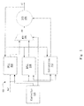
- Fig. 1 illustrates a multiple mode radio frequency synthesizer 100 according to one embodiment.
- Radio frequency synthesizer 100 generates a Local Oscillator (LO) frequency signal at a selected frequency in response to a reference (REF) signal from an external source (not shown), such as a crystal oscillator.
- radio frequency synthesizer 100 comprises a plurality of feedback loops that determines the time or phase difference between the REF signal and feedback of the LO frequency signal to generate the LO frequency signal.
- Radio frequency synthesizer 100 is a radio frequency synthesizer that has an architecture that combines a plurality of feedback loops, such as a digital frequency locked-loop (DFLL) 102 and a digital phase locked-loop (DPLL) 104, to provide complementary modes of operation.
- DFLL digital frequency locked-loop
- DPLL digital phase locked-loop
- the feedback loops of radio frequency synthesizer 100 continuously monitor the LO frequency signal from DCO 108 and perform fine adjustment of the LO frequency signal to track the frequency of the REF signal.
- the frequency F LO of the LO frequency signal is in the range of 1.1 to 1.5 GHz.
- Radio frequency synthesizer 100 further comprises a multiplexer 106, a digitally-controlled oscillator (DCO) 108, a calibration loop 112, and a controller 114.
- DCO 108 provides the Local Oscillator (LO) frequency signal that has a frequency F LO that is set by a digital frequency select control word (FW) signal from multiplexer 106.
- FW digital frequency select control word
- Controller 114 provides a selection signal to multiplexer 106 to control whether multiplexer 106 provides the FW signal from DFLL 102 or DPLL 104.
- Radio frequency synthesizer 100 may operate in a digital frequency locked-loop (DFLL) mode in which DFLL 102 controls the frequency F LO of the LO frequency signal.
- controller 114 selects the mode of operation, such as the DFLL mode or the DPLL mode, based on the reference clock frequency F REF of the REF signal. Controller 114 may select the mode of operation based on whether the reference clock frequency F REF of the REF signal exceeds a frequency threshold. In some embodiments, controller 114 selects the DFLL mode if the frequency F REF of the REF signal is low (e.g., 32 kHz).
- Radio frequency synthesizer 100 may operate in a digital phase locked-loop (DPLL) mode in which the DPLL 104 controls the frequency of the LO frequency signal.
- controller 114 selects the DPLL mode for higher-frequency reference clocks (e.g., frequencies above 1 MHz).
- calibration loop 112 provides a coarse frequency control signal to DCO 108 at the startup of radio frequency synthesizer 100 by measuring and adjusting the frequency F LO of the LO frequency signal from DCO 108.
- Calibration loop 112 may provide the coarse frequency control signal to multiplexer 106 for selective application to DCO 108.
- the calibration mode is described as being performed before the DFLL mode and the DPLL mode, the calibration mode may be performed at other times, such as when a feedback loop loses lock.
- the currently enabled loop of DFLL 102 and DPLL 104 may provide the loop that is to next be enabled with the last value of the FW signal in the currently enabled mode.
- the next to be enabled loop of DFLL 102 and DPLL 104 may use the FW signal to calculate the next frequency control FW in the next mode of operation. This may minimize the transient frequency error of the LO frequency signal while switching modes.
- calibration loop 112 may provide the coarse frequency control signal to the enabled loop of DFLL 102 and DPLL.
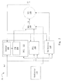
- Fig. 2 illustrates radio frequency synthesizer 100 operating in a digital frequency locked-loop mode.
- DFLL 102 comprises a counter 202 and a finite state machine (FSM) 204.
- Counter 202 monitors the LO frequency signal at a low rate.
- counter 202 is a high resolution counter.
- FSM 204 includes an algorithm for incrementing or decrementing the FW signal in response to the difference between the frequency of the LO frequency signal and a target frequency F LOT .
- FSM 204 adjusts the frequency back in the specified limit by changing the FW signal.
- the frequency F LO of the LO frequency signal tracks the frequency F REF of the REF signal with a precision in the order of 100 parts per million.
- DCO 108 may be free-running when the frequency F LO of the LO frequency signal is within the specified boundaries around the target frequency F LOT and the feedback operates in a non-linear manner to thereby provide no amplification of the reference noise.
- Fig. 3 illustrates radio frequency synthesizer 100 operating in a digital phase locked-loop mode.
- DPLL 104 comprises a phase acquisition circuit 302 and a digital processor 304.
- Phase acquisition circuit 302 monitors the phase error between the LO frequency signal and the REF signal at the reference clock rate.
- Digital processor 304 performs signal processing, such as filtering and time-to-digital conversion, to generate a correction, which is proportional to the phase error. The correction is applied to DCO 108 as the FW signal to cancel the phase error.
- digital processor 304 adjusts the frequency F LO back to the target frequency F LOT by changing the FW signal.
- radio frequency synthesizer 100 behaves as a linear feedback system.
- DPLL 104 continuously applies a correction related to a difference frequency F LO - F LOT (the difference between the frequency F LO and the target frequency F LOT ).
- DPLL 104 does not wait until the difference frequency F LO - F LOT goes beyond a specified limit.
- the magnitude of the correction applied is related to the difference frequency F LO - F LOT . This allows a tight control on the frequency F LO (e.g., 1 part per million).
- the frequency F LO of the LO frequency signal tracks the frequency F REF of the REF signal with a precision in the order of 1 part per million.
- phase acquisition circuit 302 comprises an RF counter (not shown) to increment at each clock cycle of the REF signal to provide coarse phase information as integer multiples of the period of the LO frequency signal.
- Phase acquisition circuit 302 also may comprises a time to digital converter (not shown) to measure the phase of the LO frequency signal at the clock rate of the REF signal. The time to digital converter provides fine phase information as a fraction of the oscillator period of the LO frequency signal to digital processor 304. The fine phase information may improve the phase noise performance of radio frequency synthesizer 100.
- Digital processor 304 processes the phase to lock the frequency F LO of the LO frequency signal on a multiple of the frequency of the REF signal.
- DPLL 104 may provide many advantages.
- the fast response of the feedback loop may make radio frequency synthesizer 100 more immune to external perturbations.
- the linear behavior may allow cancellation of the DCO flicker noise for better noise performance.
- Fig. 4 illustrates a simplified flowchart of a method for a calibration mode according to one embodiment.
- a startup of radio frequency synthesizer 100 is detected.
- a target LO frequency F LOT is received by controller 114.
- a frequency control signal is provided to DCO 108 by calibration loop 112 based on a comparison of the frequency F LO of the LO frequency signal to the frequency F REF of the REF signal.
- the frequency F LO of the LO frequency signal from DCO 108 is monitored by calibration loop 112.
- a determination is made by calibration loop 112 whether the frequency F LO of the LO frequency signal from DCO 108 is within a coarse frequency range based on the target LO frequency F LOT .
- the operational mode of either DFLL or DPLL is started and controlled by controller 114, if the frequency F LO of the LO frequency signal from DCO 108 is within a coarse frequency range. Otherwise, if the frequency F LO of the LO frequency signal from DCO 108 is not within a coarse frequency range, the frequency control signal is provided to DCO 108 by calibration loop 112 at 406.
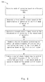
- Fig. 5 illustrates a simplified flowchart of a method for operating the radio frequency synthesizer according to one embodiment.
- a determination is made by controller 114 whether to operate radio frequency synthesizer 100 in a first mode (e.g., DFLL mode) or second mode (e.g., DPLL mode) of operation based on frequency F REF of the REF signal.
- the first mode of operation is selected if the frequency F REF of the REF signal is below a threshold
- the second mode of operation is selected if the frequency F REF of the REF signal is above the threshold.
- a first control signal is generated based on the determination of operating in the first mode of operation.
- a second control signal is generated based on the determination of operating in the second mode of operation.
- DFLL 102 is enabled to control frequency F LO of the LO frequency signal of DCO 108 based on and the first control signal.
- DPLL 104 is enabled to control the output frequency of DCO 108 based on the second control signal.
- Radio frequency synthesizer 100 may switch between the DFLL and the DPLL modes on the fly without turning off DCO 108 in a fast and relatively smooth transition, so that the switching is unnoticeable on the LO frequency signal at the output of radio frequency synthesizer 100.
Landscapes
- Stabilization Of Oscillater, Synchronisation, Frequency Synthesizers (AREA)
- Manipulation Of Pulses (AREA)
Claims (15)
- Procédé comprenant :la détermination (502) du fait d'opérer ou non dans un premier mode d'opération ou dans un deuxième mode d'opération sur base d'un signal de fréquence de référence ;en réponse à la détermination du fait d'opérer dans le premier mode d'opération, la génération (504) d'un premier signal de contrôle et l'habilitation (508) d'une boucle à asservissement de fréquence numérique (102) pour contrôler une fréquence de sortie d'un oscillateur à contrôle numérique (108) sur base du premier signal de contrôle ; eten réponse à la détermination du fait d'opérer dans le deuxième mode d'opération, la génération d'un premier signal de contrôle (504) et d'un deuxième signal de contrôle (506), et l'habilitation (510) d'une boucle à asservissement de phase numérique (104) pour contrôler la fréquence de sortie de l'oscillateur à contrôle numérique (108) sur base du deuxième signal de contrôle.
- Procédé selon la revendication 1, dans lequel la détermination du fait d'opérer ou non dans un premier mode d'opération ou dans un deuxième mode d'opération sur base d'un signal de fréquence de référence comprend :la sélection du premier mode d'opération si la fréquence de sortie sélectionnée est inférieure à un seuil ; etla sélection du deuxième mode d'opération si la fréquence de sortie sélectionnée est supérieure au seuil.
- Procédé selon l'une quelconque des revendications 1 et 2, dans lequel la boucle à asservissement de fréquence numérique contrôle en outre la fréquence de sortie de l'oscillateur à contrôle numérique dans le premier mode d'opération sur base de la fréquence de sortie de l'oscillateur à contrôle numérique et du signal de fréquence de référence.
- Procédé selon l'une quelconque des revendications 1 à 3, dans lequel la boucle à asservissement de phase numérique contrôle en outre la fréquence de sortie de l'oscillateur à contrôle numérique dans le deuxième mode d'opération sur base de la fréquence de sortie de l'oscillateur à contrôle numérique et du signal de fréquence de référence.
- Procédé selon l'une quelconque des revendications 1 à 4, comprenant en outre l'habilitation d'une boucle d'étalonnage pour contrôler la fréquence de sortie de l'oscillateur à contrôle numérique dans un mode d'opération de démarrage, le mode de démarrage se trouvant avant le premier mode d'opération et le deuxième mode d'opération.
- Procédé selon la revendication 5, dans lequel la boucle d'étalonnage contrôle en outre la fréquence de sortie de l'oscillateur à contrôle numérique dans le mode d'opération de démarrage sur base de la fréquence de sortie de l'oscillateur à contrôle numérique et du signal de fréquence de référence.
- Procédé selon la revendication 5, dans lequel la boucle d'étalonnage ajuste la fréquence de sortie de l'oscillateur à contrôle numérique pour qu'elle soit comprise dans une plage sélectionnée de la fréquence de sortie sélectionnée.
- Procédé selon l'une quelconque des revendications 1 à 7, comprenant en outre :la commutation entre le mode d'opération déterminé et un autre mode d'opération ;la déshabilitation de la boucle d'asservissement habilitée ; etl'habilitation de l'autre boucle d'asservissement.
- Procédé selon la revendication 8, comprenant en outre la fourniture d'un signal indicateur d'une commande de fréquence récente provenant de la boucle d'asservissement préalablement habilitée avant la commutation.
- Circuit comprenant :un oscillateur à contrôle numérique configuré pour générer un signal d'oscillateur ayant une fréquence de sortie ;une boucle à asservissement de fréquence numérique configurée pour contrôler la fréquence de sortie du signal d'oscillateur dans un premier mode d'opération sur base d'un premier signal de contrôle ;une boucle à asservissement de phase numérique configurée pour contrôler la fréquence de sortie du signal d'oscillateur dans un deuxième mode d'opération sur base d'un deuxième signal de contrôle ; etun contrôleur configuré pour :déterminer s'il faut ou non opérer dans le premier mode ou dans le deuxième mode d'opération sur base d'un signal de fréquence de référence ;en réponse à la détermination du fait d'opérer dans le premier mode d'opération, générer le premier signal de contrôle ; eten réponse à la détermination du fait d'opérer dans le deuxième mode d'opération, générer le deuxième signal de contrôle.
- Circuit selon la revendication 10, dans lequel le contrôleur est en outre configuré pour :sélectionner le premier mode d'opération si le signal de fréquence de référence est inférieur à un seuil ; etsélectionner le deuxième mode d'opération si le signal de fréquence de référence est supérieur au premier seuil.
- Circuit selon la revendication 10 ou 11, dans lequel la boucle à asservissement de fréquence numérique est en outre configurée pour contrôler la fréquence de sortie du signal d'oscillateur dans le premier mode d'opération sur base de la fréquence de sortie et du signal de fréquence de référence.
- Circuit selon l'une quelconque des revendications 10 à 12, dans lequel la boucle à asservissement de phase numérique est en outre configurée pour contrôler la fréquence de sortie du signal d'oscillateur dans le deuxième mode d'opération sur base de la fréquence de sortie et du signal de fréquence de référence ; ou
comprenant en outre une boucle d'étalonnage configurée pour contrôler la fréquence de sortie du signal d'oscillateur dans un mode d'opération de démarrage, le mode de démarrage se trouvant avant le premier mode d'opération et le deuxième mode d'opération ; ou
dans lequel la boucle d'étalonnage est en outre configurée pour contrôler la fréquence de sortie du signal d'oscillateur dans le mode d'opération de démarrage sur base de la fréquence de sortie et du signal de fréquence de référence. - Circuit selon la revendication 13, dans lequel la boucle d'étalonnage est en outre configurée pour contrôler la fréquence de sortie du signal d'oscillateur pour qu'elle soit comprise dans une plage sélectionnée de la fréquence de sortie sélectionnée.
- Circuit selon la revendication 10, dans lequel le contrôleur est en outre configuré pour :commuter entre le mode d'opération déterminé et un autre mode d'opération ;déshabiliter la boucle d'asservissement habilitée ; ethabiliter l'autre boucle ; et/oudans lequel le contrôleur est en outre configuré pour fournir un signal indicateur d'une commande de fréquence récente provenant de la boucle d'asservissement préalablement habilitée avant la commutation.
Applications Claiming Priority (2)
| Application Number | Priority Date | Filing Date | Title |
|---|---|---|---|
| US201161447369P | 2011-02-28 | 2011-02-28 | |
| PCT/IB2012/002369 WO2013014541A2 (fr) | 2011-02-28 | 2012-02-27 | Procédés et dispositifs pour synthétiseurs de radiofréquences à modes multiples |
Publications (3)
| Publication Number | Publication Date |
|---|---|
| EP2681966A2 EP2681966A2 (fr) | 2014-01-08 |
| EP2681966A4 EP2681966A4 (fr) | 2015-01-21 |
| EP2681966B1 true EP2681966B1 (fr) | 2016-10-05 |
Family
ID=46718559
Family Applications (2)
| Application Number | Title | Priority Date | Filing Date |
|---|---|---|---|
| EP12752654.9A Not-in-force EP2681844B1 (fr) | 2011-02-28 | 2012-02-27 | Procédés et dispositifs permettant de mettre en uvre une boucle à verrouillage de phase entièrement numérique |
| EP12818045.2A Not-in-force EP2681966B1 (fr) | 2011-02-28 | 2012-02-27 | Procédés et dispositifs pour synthétiseurs de radiofréquences à modes multiples |
Family Applications Before (1)
| Application Number | Title | Priority Date | Filing Date |
|---|---|---|---|
| EP12752654.9A Not-in-force EP2681844B1 (fr) | 2011-02-28 | 2012-02-27 | Procédés et dispositifs permettant de mettre en uvre une boucle à verrouillage de phase entièrement numérique |
Country Status (3)
| Country | Link |
|---|---|
| US (4) | US9036763B2 (fr) |
| EP (2) | EP2681844B1 (fr) |
| WO (2) | WO2013014541A2 (fr) |
Cited By (1)
| Publication number | Priority date | Publication date | Assignee | Title |
|---|---|---|---|---|
| US10802127B2 (en) * | 2016-08-01 | 2020-10-13 | Vega Grieshaber Kg | Radar fill level measurement device |
Families Citing this family (19)
| Publication number | Priority date | Publication date | Assignee | Title |
|---|---|---|---|---|
| US10127612B2 (en) * | 2012-05-03 | 2018-11-13 | Tamer Trading Technologies Llc | System, method, and computer-readable medium for improving the efficiency and stability of financial markets |
| TWI489782B (zh) * | 2012-10-30 | 2015-06-21 | Realtek Semiconductor Corp | 相位校正裝置及相位校正方法 |
| US9641183B2 (en) * | 2013-10-22 | 2017-05-02 | The Regents Of The University Of Michigan | Dual-loop programmable and dividerless clock generator for ultra low power applications |
| EP3072266B1 (fr) * | 2013-11-19 | 2019-01-09 | The Regents of The University of California | Interface d'enregistrement électro-physique résistante à la saturation |
| US9148153B2 (en) * | 2013-12-30 | 2015-09-29 | Intel Corporation | Systems and methods for frequency domain calibration and characterization |
| US9391624B1 (en) * | 2014-06-26 | 2016-07-12 | Marvell International Ltd. | Method and apparatus for avoiding dead zone effects in digital phase locked loops |
| DE102015102600A1 (de) * | 2015-02-24 | 2016-08-25 | Infineon Technologies Ag | Kommunikationsvorrichtung und Verfahren zum Kalibrieren eines Oszillators |
| US9419629B1 (en) * | 2016-03-01 | 2016-08-16 | Freescale Semiconductor, Inc. | Delay-locked loop circuit with fractional phase frequency detector |
| US10359995B2 (en) | 2016-04-29 | 2019-07-23 | Texas Instruments Incorporated | Architecture and instruction set to support integer division |
| US10635395B2 (en) | 2016-06-30 | 2020-04-28 | Texas Instruments Incorporated | Architecture and instruction set to support interruptible floating point division |
| US9628262B1 (en) * | 2016-07-19 | 2017-04-18 | Texas Instruments Incorporated | Spur reduction in phase locked loops using reference clock dithering |
| WO2018125046A1 (fr) * | 2016-12-27 | 2018-07-05 | Intel Corporation | Architecture pll fractionnaire sans diviseur |
| US10057046B1 (en) * | 2017-02-22 | 2018-08-21 | SiTune Corporation | Dynamic calibration for transceivers |
| DE112017007155T5 (de) | 2017-03-02 | 2019-11-28 | Intel IP Corporation | Zeit-zu-digital-wandler, digitale phasenregelschleife, verfahren zum betreiben eines zeit-zu-digital-wandlers und verfahren für eine digitale phasenregelschleife |
| JP6939261B2 (ja) * | 2017-08-29 | 2021-09-22 | セイコーエプソン株式会社 | 時間デジタル変換回路、回路装置、物理量測定装置、電子機器及び移動体 |
| US10826505B1 (en) * | 2019-06-24 | 2020-11-03 | Nxp B.V. | All digital phase locked loop (ADPLL) with frequency locked loop |
| GB201918967D0 (en) | 2019-12-20 | 2020-02-05 | Nordic Semiconductor Asa | Clock circuit portions |
| US11398812B1 (en) * | 2021-09-25 | 2022-07-26 | Qualcomm Incorporated | Adaptive clock duty-cycle controller |
| CN116318195B (zh) * | 2022-11-23 | 2025-08-26 | 上海美仁半导体有限公司 | 射频控制电路及其控制方法、装置、芯片和电子设备 |
Family Cites Families (23)
| Publication number | Priority date | Publication date | Assignee | Title |
|---|---|---|---|---|
| JP3433021B2 (ja) * | 1996-09-20 | 2003-08-04 | パイオニア株式会社 | Pll回路 |
| US6307413B1 (en) * | 1999-12-23 | 2001-10-23 | Cypress Semiconductor Corp. | Reference-free clock generator and data recovery PLL |
| US6310521B1 (en) * | 1999-12-23 | 2001-10-30 | Cypress Semiconductor Corp. | Reference-free clock generation and data recovery PLL |
| US6683930B1 (en) * | 1999-12-23 | 2004-01-27 | Cypress Semiconductor Corp. | Digital phase/frequency detector, and clock generator and data recovery PLL containing the same |
| JP4454798B2 (ja) * | 2000-06-09 | 2010-04-21 | Necエレクトロニクス株式会社 | クロック再生装置 |
| US8385476B2 (en) * | 2001-04-25 | 2013-02-26 | Texas Instruments Incorporated | Digital phase locked loop |
| US7009456B2 (en) * | 2003-08-04 | 2006-03-07 | Agere Systems Inc. | PLL employing a sample-based capacitance multiplier |
| US6867627B1 (en) * | 2003-09-16 | 2005-03-15 | Integrated Device Technology, Inc. | Delay-locked loop (DLL) integrated circuits having high bandwidth and reliable locking characteristics |
| US6949981B2 (en) | 2004-02-18 | 2005-09-27 | International Business Machines Corporation | Dynamic threshold for VCO calibration |
| US6987406B1 (en) * | 2004-05-17 | 2006-01-17 | National Semiconductor Corporation | Wide frequency range phase-locked loop circuit with phase difference |
| TWI241069B (en) * | 2004-11-12 | 2005-10-01 | Ind Tech Res Inst | Automatically calibrated frequency-synthesis apparatus |
| US7750685B1 (en) * | 2005-03-17 | 2010-07-06 | Rf Micro Devices, Inc. | Frequency measurement based frequency locked loop synthesizer |
| KR100714579B1 (ko) * | 2005-11-25 | 2007-05-07 | 삼성전기주식회사 | 잡음 특성이 향상된 위상 주파수 검출기 |
| KR100793988B1 (ko) * | 2006-04-21 | 2008-01-16 | 삼성전자주식회사 | 자기 교정 전압 제어 발진기를 위한 시스템 및 방법 |
| US7616069B2 (en) | 2006-12-06 | 2009-11-10 | Broadcom Corporation | Method and system for fast PLL close-loop settling after open-loop VCO calibration |
| US7888973B1 (en) * | 2007-06-05 | 2011-02-15 | Marvell International Ltd. | Matrix time-to-digital conversion frequency synthesizer |
| DE102007027331B4 (de) | 2007-06-14 | 2016-10-20 | Texas Instruments Deutschland Gmbh | Phasenregelkreis mit zweistufiger Steuerung |
| US8045670B2 (en) | 2007-06-22 | 2011-10-25 | Texas Instruments Incorporated | Interpolative all-digital phase locked loop |
| US8269563B2 (en) * | 2008-06-10 | 2012-09-18 | Qualcomm Incorporated | Dithering a digitally-controlled oscillator output in a phase-locked loop |
| US8165258B2 (en) * | 2008-08-11 | 2012-04-24 | Himax Technologies Limited | Clock generating device and method thereof |
| CN102187579A (zh) * | 2008-10-23 | 2011-09-14 | 松下电器产业株式会社 | 数字pll电路及通信装置 |
| EP2237418B1 (fr) | 2009-04-03 | 2017-10-04 | Nxp B.V. | Synthétiseur de fréquences |
| JP2010273118A (ja) | 2009-05-21 | 2010-12-02 | Toshiba Corp | 時間デジタル変換器 |
-
2012
- 2012-02-27 EP EP12752654.9A patent/EP2681844B1/fr not_active Not-in-force
- 2012-02-27 US US13/406,342 patent/US9036763B2/en active Active
- 2012-02-27 WO PCT/IB2012/002369 patent/WO2013014541A2/fr not_active Ceased
- 2012-02-27 EP EP12818045.2A patent/EP2681966B1/fr not_active Not-in-force
- 2012-02-27 WO PCT/IB2012/000467 patent/WO2012117295A2/fr not_active Ceased
- 2012-02-27 US US13/406,246 patent/US8710884B2/en not_active Expired - Fee Related
-
2014
- 2014-04-03 US US14/244,710 patent/US8957713B2/en active Active
-
2015
- 2015-05-15 US US14/713,945 patent/US9306586B2/en active Active
Cited By (1)
| Publication number | Priority date | Publication date | Assignee | Title |
|---|---|---|---|---|
| US10802127B2 (en) * | 2016-08-01 | 2020-10-13 | Vega Grieshaber Kg | Radar fill level measurement device |
Also Published As
| Publication number | Publication date |
|---|---|
| WO2013014541A3 (fr) | 2013-06-06 |
| EP2681844A2 (fr) | 2014-01-08 |
| WO2012117295A2 (fr) | 2012-09-07 |
| US9036763B2 (en) | 2015-05-19 |
| EP2681966A4 (fr) | 2015-01-21 |
| WO2012117295A3 (fr) | 2013-01-03 |
| US20120328065A1 (en) | 2012-12-27 |
| US9306586B2 (en) | 2016-04-05 |
| EP2681844B1 (fr) | 2018-06-13 |
| US20150249455A1 (en) | 2015-09-03 |
| EP2681966A2 (fr) | 2014-01-08 |
| US20120218014A1 (en) | 2012-08-30 |
| US8957713B2 (en) | 2015-02-17 |
| EP2681844A4 (fr) | 2015-02-18 |
| US8710884B2 (en) | 2014-04-29 |
| US20140218086A1 (en) | 2014-08-07 |
| WO2013014541A2 (fr) | 2013-01-31 |
Similar Documents
| Publication | Publication Date | Title |
|---|---|---|
| EP2681966B1 (fr) | Procédés et dispositifs pour synthétiseurs de radiofréquences à modes multiples | |
| US10727844B1 (en) | Reference clock frequency change handling in a phase-locked loop | |
| US7573303B1 (en) | Digitally controlled system on-chip (SOC) clock generator | |
| US7701299B2 (en) | Low phase noise PLL synthesizer | |
| JP5420641B2 (ja) | デジタル位相ロックループ(dpll)における電力消費を制御するシステム及び方法 | |
| US20110291706A1 (en) | Elimination of fractional n boundary spurs in a signal synthesizer | |
| US7884657B2 (en) | Oscillation frequency control circuit | |
| JP4355350B2 (ja) | 発振周波数制御回路 | |
| US10826505B1 (en) | All digital phase locked loop (ADPLL) with frequency locked loop | |
| US11031942B2 (en) | Frequency generator and associated method | |
| WO2019060123A1 (fr) | Gestion de phase d'horloge de système sur puce à l'aide de pll à division fractionnaire par n | |
| US20130057327A1 (en) | Reducing phase locked loop phase lock time | |
| EP2066035A1 (fr) | Circuit de commande de fréquence d'oscillation | |
| US8666012B2 (en) | Operating a frequency synthesizer | |
| US8629728B2 (en) | VCO control circuit and method thereof, fast locking PLL and method for fast locking PLL | |
| US10693475B1 (en) | Gradual frequency transition with a frequency step | |
| JP2012075000A (ja) | 位相同期回路及び無線機 | |
| US10270487B2 (en) | Frequency generator and associated method | |
| JP2007189455A (ja) | 位相比較回路およびそれを用いたpll周波数シンセサイザ | |
| CN110429935B (zh) | 一种切频锁相回路及其所运用的算法 | |
| CA2364506A1 (fr) | Systemes et circuits integres de synchronisation | |
| KR20170094431A (ko) | 오실레이터 캘리브레이션 | |
| KR101752599B1 (ko) | 주파수 합성기 | |
| US9350364B1 (en) | Phase-locked loop circuit having low close-in phase noise | |
| JP2011199339A (ja) | Pll回路 |
Legal Events
| Date | Code | Title | Description |
|---|---|---|---|
| PUAI | Public reference made under article 153(3) epc to a published international application that has entered the european phase |
Free format text: ORIGINAL CODE: 0009012 |
|
| 17P | Request for examination filed |
Effective date: 20130827 |
|
| AK | Designated contracting states |
Kind code of ref document: A2 Designated state(s): AL AT BE BG CH CY CZ DE DK EE ES FI FR GB GR HR HU IE IS IT LI LT LU LV MC MK MT NL NO PL PT RO RS SE SI SK SM TR |
|
| DAX | Request for extension of the european patent (deleted) | ||
| RIC1 | Information provided on ipc code assigned before grant |
Ipc: H03L 7/06 20060101AFI20140801BHEP |
|
| REG | Reference to a national code |
Ref country code: DE Ref legal event code: R079 Ref document number: 602012023841 Country of ref document: DE Free format text: PREVIOUS MAIN CLASS: H04W0088020000 Ipc: H03L0007060000 |
|
| A4 | Supplementary search report drawn up and despatched |
Effective date: 20150105 |
|
| RIC1 | Information provided on ipc code assigned before grant |
Ipc: H03L 7/06 20060101AFI20141218BHEP Ipc: H03L 7/16 20060101ALI20141218BHEP Ipc: H03L 7/099 20060101ALI20141218BHEP |
|
| GRAP | Despatch of communication of intention to grant a patent |
Free format text: ORIGINAL CODE: EPIDOSNIGR1 |
|
| INTG | Intention to grant announced |
Effective date: 20160426 |
|
| GRAS | Grant fee paid |
Free format text: ORIGINAL CODE: EPIDOSNIGR3 |
|
| GRAA | (expected) grant |
Free format text: ORIGINAL CODE: 0009210 |
|
| AK | Designated contracting states |
Kind code of ref document: B1 Designated state(s): AL AT BE BG CH CY CZ DE DK EE ES FI FR GB GR HR HU IE IS IT LI LT LU LV MC MK MT NL NO PL PT RO RS SE SI SK SM TR |
|
| REG | Reference to a national code |
Ref country code: GB Ref legal event code: FG4D |
|
| REG | Reference to a national code |
Ref country code: CH Ref legal event code: EP |
|
| REG | Reference to a national code |
Ref country code: AT Ref legal event code: REF Ref document number: 835386 Country of ref document: AT Kind code of ref document: T Effective date: 20161015 |
|
| REG | Reference to a national code |
Ref country code: IE Ref legal event code: FG4D |
|
| REG | Reference to a national code |
Ref country code: DE Ref legal event code: R096 Ref document number: 602012023841 Country of ref document: DE |
|
| REG | Reference to a national code |
Ref country code: NL Ref legal event code: MP Effective date: 20161005 |
|
| REG | Reference to a national code |
Ref country code: LT Ref legal event code: MG4D |
|
| REG | Reference to a national code |
Ref country code: FR Ref legal event code: PLFP Year of fee payment: 6 |
|
| PG25 | Lapsed in a contracting state [announced via postgrant information from national office to epo] |
Ref country code: LV Free format text: LAPSE BECAUSE OF FAILURE TO SUBMIT A TRANSLATION OF THE DESCRIPTION OR TO PAY THE FEE WITHIN THE PRESCRIBED TIME-LIMIT Effective date: 20161005 |
|
| REG | Reference to a national code |
Ref country code: AT Ref legal event code: MK05 Ref document number: 835386 Country of ref document: AT Kind code of ref document: T Effective date: 20161005 |
|
| PG25 | Lapsed in a contracting state [announced via postgrant information from national office to epo] |
Ref country code: GR Free format text: LAPSE BECAUSE OF FAILURE TO SUBMIT A TRANSLATION OF THE DESCRIPTION OR TO PAY THE FEE WITHIN THE PRESCRIBED TIME-LIMIT Effective date: 20170106 Ref country code: SE Free format text: LAPSE BECAUSE OF FAILURE TO SUBMIT A TRANSLATION OF THE DESCRIPTION OR TO PAY THE FEE WITHIN THE PRESCRIBED TIME-LIMIT Effective date: 20161005 Ref country code: LT Free format text: LAPSE BECAUSE OF FAILURE TO SUBMIT A TRANSLATION OF THE DESCRIPTION OR TO PAY THE FEE WITHIN THE PRESCRIBED TIME-LIMIT Effective date: 20161005 Ref country code: NO Free format text: LAPSE BECAUSE OF FAILURE TO SUBMIT A TRANSLATION OF THE DESCRIPTION OR TO PAY THE FEE WITHIN THE PRESCRIBED TIME-LIMIT Effective date: 20170105 |
|
| PG25 | Lapsed in a contracting state [announced via postgrant information from national office to epo] |
Ref country code: PL Free format text: LAPSE BECAUSE OF FAILURE TO SUBMIT A TRANSLATION OF THE DESCRIPTION OR TO PAY THE FEE WITHIN THE PRESCRIBED TIME-LIMIT Effective date: 20161005 Ref country code: PT Free format text: LAPSE BECAUSE OF FAILURE TO SUBMIT A TRANSLATION OF THE DESCRIPTION OR TO PAY THE FEE WITHIN THE PRESCRIBED TIME-LIMIT Effective date: 20170206 Ref country code: ES Free format text: LAPSE BECAUSE OF FAILURE TO SUBMIT A TRANSLATION OF THE DESCRIPTION OR TO PAY THE FEE WITHIN THE PRESCRIBED TIME-LIMIT Effective date: 20161005 Ref country code: HR Free format text: LAPSE BECAUSE OF FAILURE TO SUBMIT A TRANSLATION OF THE DESCRIPTION OR TO PAY THE FEE WITHIN THE PRESCRIBED TIME-LIMIT Effective date: 20161005 Ref country code: FI Free format text: LAPSE BECAUSE OF FAILURE TO SUBMIT A TRANSLATION OF THE DESCRIPTION OR TO PAY THE FEE WITHIN THE PRESCRIBED TIME-LIMIT Effective date: 20161005 Ref country code: AT Free format text: LAPSE BECAUSE OF FAILURE TO SUBMIT A TRANSLATION OF THE DESCRIPTION OR TO PAY THE FEE WITHIN THE PRESCRIBED TIME-LIMIT Effective date: 20161005 Ref country code: RS Free format text: LAPSE BECAUSE OF FAILURE TO SUBMIT A TRANSLATION OF THE DESCRIPTION OR TO PAY THE FEE WITHIN THE PRESCRIBED TIME-LIMIT Effective date: 20161005 Ref country code: IS Free format text: LAPSE BECAUSE OF FAILURE TO SUBMIT A TRANSLATION OF THE DESCRIPTION OR TO PAY THE FEE WITHIN THE PRESCRIBED TIME-LIMIT Effective date: 20170205 Ref country code: BE Free format text: LAPSE BECAUSE OF FAILURE TO SUBMIT A TRANSLATION OF THE DESCRIPTION OR TO PAY THE FEE WITHIN THE PRESCRIBED TIME-LIMIT Effective date: 20161005 Ref country code: NL Free format text: LAPSE BECAUSE OF FAILURE TO SUBMIT A TRANSLATION OF THE DESCRIPTION OR TO PAY THE FEE WITHIN THE PRESCRIBED TIME-LIMIT Effective date: 20161005 |
|
| REG | Reference to a national code |
Ref country code: DE Ref legal event code: R097 Ref document number: 602012023841 Country of ref document: DE |
|
| PG25 | Lapsed in a contracting state [announced via postgrant information from national office to epo] |
Ref country code: CZ Free format text: LAPSE BECAUSE OF FAILURE TO SUBMIT A TRANSLATION OF THE DESCRIPTION OR TO PAY THE FEE WITHIN THE PRESCRIBED TIME-LIMIT Effective date: 20161005 Ref country code: SK Free format text: LAPSE BECAUSE OF FAILURE TO SUBMIT A TRANSLATION OF THE DESCRIPTION OR TO PAY THE FEE WITHIN THE PRESCRIBED TIME-LIMIT Effective date: 20161005 Ref country code: DK Free format text: LAPSE BECAUSE OF FAILURE TO SUBMIT A TRANSLATION OF THE DESCRIPTION OR TO PAY THE FEE WITHIN THE PRESCRIBED TIME-LIMIT Effective date: 20161005 Ref country code: RO Free format text: LAPSE BECAUSE OF FAILURE TO SUBMIT A TRANSLATION OF THE DESCRIPTION OR TO PAY THE FEE WITHIN THE PRESCRIBED TIME-LIMIT Effective date: 20161005 Ref country code: EE Free format text: LAPSE BECAUSE OF FAILURE TO SUBMIT A TRANSLATION OF THE DESCRIPTION OR TO PAY THE FEE WITHIN THE PRESCRIBED TIME-LIMIT Effective date: 20161005 |
|
| PLBE | No opposition filed within time limit |
Free format text: ORIGINAL CODE: 0009261 |
|
| STAA | Information on the status of an ep patent application or granted ep patent |
Free format text: STATUS: NO OPPOSITION FILED WITHIN TIME LIMIT |
|
| PG25 | Lapsed in a contracting state [announced via postgrant information from national office to epo] |
Ref country code: BG Free format text: LAPSE BECAUSE OF FAILURE TO SUBMIT A TRANSLATION OF THE DESCRIPTION OR TO PAY THE FEE WITHIN THE PRESCRIBED TIME-LIMIT Effective date: 20170105 Ref country code: IT Free format text: LAPSE BECAUSE OF FAILURE TO SUBMIT A TRANSLATION OF THE DESCRIPTION OR TO PAY THE FEE WITHIN THE PRESCRIBED TIME-LIMIT Effective date: 20161005 Ref country code: SM Free format text: LAPSE BECAUSE OF FAILURE TO SUBMIT A TRANSLATION OF THE DESCRIPTION OR TO PAY THE FEE WITHIN THE PRESCRIBED TIME-LIMIT Effective date: 20161005 |
|
| 26N | No opposition filed |
Effective date: 20170706 |
|
| PG25 | Lapsed in a contracting state [announced via postgrant information from national office to epo] |
Ref country code: MC Free format text: LAPSE BECAUSE OF FAILURE TO SUBMIT A TRANSLATION OF THE DESCRIPTION OR TO PAY THE FEE WITHIN THE PRESCRIBED TIME-LIMIT Effective date: 20161005 |
|
| REG | Reference to a national code |
Ref country code: CH Ref legal event code: PL |
|
| PG25 | Lapsed in a contracting state [announced via postgrant information from national office to epo] |
Ref country code: LI Free format text: LAPSE BECAUSE OF NON-PAYMENT OF DUE FEES Effective date: 20170228 Ref country code: CH Free format text: LAPSE BECAUSE OF NON-PAYMENT OF DUE FEES Effective date: 20170228 |
|
| REG | Reference to a national code |
Ref country code: IE Ref legal event code: MM4A |
|
| PG25 | Lapsed in a contracting state [announced via postgrant information from national office to epo] |
Ref country code: SI Free format text: LAPSE BECAUSE OF FAILURE TO SUBMIT A TRANSLATION OF THE DESCRIPTION OR TO PAY THE FEE WITHIN THE PRESCRIBED TIME-LIMIT Effective date: 20161005 |
|
| PG25 | Lapsed in a contracting state [announced via postgrant information from national office to epo] |
Ref country code: LU Free format text: LAPSE BECAUSE OF NON-PAYMENT OF DUE FEES Effective date: 20170227 |
|
| REG | Reference to a national code |
Ref country code: FR Ref legal event code: PLFP Year of fee payment: 7 |
|
| PG25 | Lapsed in a contracting state [announced via postgrant information from national office to epo] |
Ref country code: IE Free format text: LAPSE BECAUSE OF NON-PAYMENT OF DUE FEES Effective date: 20170227 |
|
| PG25 | Lapsed in a contracting state [announced via postgrant information from national office to epo] |
Ref country code: MT Free format text: LAPSE BECAUSE OF NON-PAYMENT OF DUE FEES Effective date: 20170227 |
|
| PGFP | Annual fee paid to national office [announced via postgrant information from national office to epo] |
Ref country code: GB Payment date: 20190227 Year of fee payment: 8 |
|
| PGFP | Annual fee paid to national office [announced via postgrant information from national office to epo] |
Ref country code: FR Payment date: 20190226 Year of fee payment: 8 |
|
| PG25 | Lapsed in a contracting state [announced via postgrant information from national office to epo] |
Ref country code: HU Free format text: LAPSE BECAUSE OF FAILURE TO SUBMIT A TRANSLATION OF THE DESCRIPTION OR TO PAY THE FEE WITHIN THE PRESCRIBED TIME-LIMIT; INVALID AB INITIO Effective date: 20120227 |
|
| PGFP | Annual fee paid to national office [announced via postgrant information from national office to epo] |
Ref country code: DE Payment date: 20190426 Year of fee payment: 8 |
|
| PG25 | Lapsed in a contracting state [announced via postgrant information from national office to epo] |
Ref country code: CY Free format text: LAPSE BECAUSE OF NON-PAYMENT OF DUE FEES Effective date: 20161005 |
|
| PG25 | Lapsed in a contracting state [announced via postgrant information from national office to epo] |
Ref country code: MK Free format text: LAPSE BECAUSE OF FAILURE TO SUBMIT A TRANSLATION OF THE DESCRIPTION OR TO PAY THE FEE WITHIN THE PRESCRIBED TIME-LIMIT Effective date: 20161005 |
|
| PG25 | Lapsed in a contracting state [announced via postgrant information from national office to epo] |
Ref country code: TR Free format text: LAPSE BECAUSE OF FAILURE TO SUBMIT A TRANSLATION OF THE DESCRIPTION OR TO PAY THE FEE WITHIN THE PRESCRIBED TIME-LIMIT Effective date: 20161005 |
|
| REG | Reference to a national code |
Ref country code: DE Ref legal event code: R082 Ref document number: 602012023841 Country of ref document: DE Representative=s name: GRUENECKER PATENT- UND RECHTSANWAELTE PARTG MB, DE Ref country code: DE Ref legal event code: R081 Ref document number: 602012023841 Country of ref document: DE Owner name: MARVELL ASIA PTE, LTD., SG Free format text: FORMER OWNER: MARVELL WORLD TRADE LTD., ST. MICHAEL, BB |
|
| PG25 | Lapsed in a contracting state [announced via postgrant information from national office to epo] |
Ref country code: AL Free format text: LAPSE BECAUSE OF FAILURE TO SUBMIT A TRANSLATION OF THE DESCRIPTION OR TO PAY THE FEE WITHIN THE PRESCRIBED TIME-LIMIT Effective date: 20161005 |
|
| REG | Reference to a national code |
Ref country code: GB Ref legal event code: 732E Free format text: REGISTERED BETWEEN 20200709 AND 20200715 |
|
| REG | Reference to a national code |
Ref country code: DE Ref legal event code: R119 Ref document number: 602012023841 Country of ref document: DE |
|
| GBPC | Gb: european patent ceased through non-payment of renewal fee |
Effective date: 20200227 |
|
| PG25 | Lapsed in a contracting state [announced via postgrant information from national office to epo] |
Ref country code: DE Free format text: LAPSE BECAUSE OF NON-PAYMENT OF DUE FEES Effective date: 20200901 Ref country code: GB Free format text: LAPSE BECAUSE OF NON-PAYMENT OF DUE FEES Effective date: 20200227 Ref country code: FR Free format text: LAPSE BECAUSE OF NON-PAYMENT OF DUE FEES Effective date: 20200229 |