EP2682367A2 - Verfahren zur n-dotierung von graphen - Google Patents
Verfahren zur n-dotierung von graphen Download PDFInfo
- Publication number
- EP2682367A2 EP2682367A2 EP12753018.6A EP12753018A EP2682367A2 EP 2682367 A2 EP2682367 A2 EP 2682367A2 EP 12753018 A EP12753018 A EP 12753018A EP 2682367 A2 EP2682367 A2 EP 2682367A2
- Authority
- EP
- European Patent Office
- Prior art keywords
- graphene
- doping
- type dopant
- doped
- substrate
- Prior art date
- Legal status (The legal status is an assumption and is not a legal conclusion. Google has not performed a legal analysis and makes no representation as to the accuracy of the status listed.)
- Withdrawn
Links
Images


Classifications
-
- C—CHEMISTRY; METALLURGY
- C01—INORGANIC CHEMISTRY
- C01B—NON-METALLIC ELEMENTS; COMPOUNDS THEREOF; METALLOIDS OR COMPOUNDS THEREOF NOT COVERED BY SUBCLASS C01C
- C01B32/00—Carbon; Compounds thereof
- C01B32/15—Nano-sized carbon materials
- C01B32/182—Graphene
- C01B32/194—After-treatment
-
- H—ELECTRICITY
- H10—SEMICONDUCTOR DEVICES; ELECTRIC SOLID-STATE DEVICES NOT OTHERWISE PROVIDED FOR
- H10P—GENERIC PROCESSES OR APPARATUS FOR THE MANUFACTURE OR TREATMENT OF DEVICES COVERED BY CLASS H10
- H10P95/00—Generic processes or apparatus for manufacture or treatments not covered by the other groups of this subclass
- H10P95/92—Formation of n- or p-type semiconductors, e.g. doping of graphene
-
- B—PERFORMING OPERATIONS; TRANSPORTING
- B82—NANOTECHNOLOGY
- B82Y—SPECIFIC USES OR APPLICATIONS OF NANOSTRUCTURES; MEASUREMENT OR ANALYSIS OF NANOSTRUCTURES; MANUFACTURE OR TREATMENT OF NANOSTRUCTURES
- B82Y30/00—Nanotechnology for materials or surface science, e.g. nanocomposites
-
- B—PERFORMING OPERATIONS; TRANSPORTING
- B82—NANOTECHNOLOGY
- B82Y—SPECIFIC USES OR APPLICATIONS OF NANOSTRUCTURES; MEASUREMENT OR ANALYSIS OF NANOSTRUCTURES; MANUFACTURE OR TREATMENT OF NANOSTRUCTURES
- B82Y40/00—Manufacture or treatment of nanostructures
-
- H—ELECTRICITY
- H10—SEMICONDUCTOR DEVICES; ELECTRIC SOLID-STATE DEVICES NOT OTHERWISE PROVIDED FOR
- H10D—INORGANIC ELECTRIC SEMICONDUCTOR DEVICES
- H10D62/00—Semiconductor bodies, or regions thereof, of devices having potential barriers
- H10D62/80—Semiconductor bodies, or regions thereof, of devices having potential barriers characterised by the materials
- H10D62/881—Semiconductor bodies, or regions thereof, of devices having potential barriers characterised by the materials being a two-dimensional material
- H10D62/882—Graphene
-
- H—ELECTRICITY
- H10—SEMICONDUCTOR DEVICES; ELECTRIC SOLID-STATE DEVICES NOT OTHERWISE PROVIDED FOR
- H10P—GENERIC PROCESSES OR APPARATUS FOR THE MANUFACTURE OR TREATMENT OF DEVICES COVERED BY CLASS H10
- H10P14/00—Formation of materials, e.g. in the shape of layers or pillars
- H10P14/20—Formation of materials, e.g. in the shape of layers or pillars of semiconductor materials
- H10P14/24—Formation of materials, e.g. in the shape of layers or pillars of semiconductor materials using chemical vapour deposition [CVD]
-
- H—ELECTRICITY
- H10—SEMICONDUCTOR DEVICES; ELECTRIC SOLID-STATE DEVICES NOT OTHERWISE PROVIDED FOR
- H10P—GENERIC PROCESSES OR APPARATUS FOR THE MANUFACTURE OR TREATMENT OF DEVICES COVERED BY CLASS H10
- H10P14/00—Formation of materials, e.g. in the shape of layers or pillars
- H10P14/20—Formation of materials, e.g. in the shape of layers or pillars of semiconductor materials
- H10P14/34—Deposited materials, e.g. layers
- H10P14/3402—Deposited materials, e.g. layers characterised by the chemical composition
- H10P14/3404—Deposited materials, e.g. layers characterised by the chemical composition being Group IVA materials
- H10P14/3406—Carbon, e.g. diamond-like carbon
-
- H—ELECTRICITY
- H10—SEMICONDUCTOR DEVICES; ELECTRIC SOLID-STATE DEVICES NOT OTHERWISE PROVIDED FOR
- H10P—GENERIC PROCESSES OR APPARATUS FOR THE MANUFACTURE OR TREATMENT OF DEVICES COVERED BY CLASS H10
- H10P32/00—Diffusion of dopants within, into or out of wafers, substrates or parts of devices
-
- H—ELECTRICITY
- H10—SEMICONDUCTOR DEVICES; ELECTRIC SOLID-STATE DEVICES NOT OTHERWISE PROVIDED FOR
- H10W—GENERIC PACKAGES, INTERCONNECTIONS, CONNECTORS OR OTHER CONSTRUCTIONAL DETAILS OF DEVICES COVERED BY CLASS H10
- H10W10/00—Isolation regions in semiconductor bodies between components of integrated devices
- H10W10/01—Manufacture or treatment
- H10W10/031—Manufacture or treatment of isolation regions comprising PN junctions
-
- H—ELECTRICITY
- H10—SEMICONDUCTOR DEVICES; ELECTRIC SOLID-STATE DEVICES NOT OTHERWISE PROVIDED FOR
- H10W—GENERIC PACKAGES, INTERCONNECTIONS, CONNECTORS OR OTHER CONSTRUCTIONAL DETAILS OF DEVICES COVERED BY CLASS H10
- H10W10/00—Isolation regions in semiconductor bodies between components of integrated devices
- H10W10/30—Isolation regions comprising PN junctions
Definitions
- the present disclosure relates to an n-doping method of a graphene by a doping solution containing an n-type dopant or a vapor containing an n-type dopant, an n-doped graphene prepared by the method, and a device using the same.
- Fullerene, carbon nanotubes, graphene, graphite, and the like are low-dimensional nano-materials composed of carbon atoms. That is, carbon atoms arranged in a hexagonal shape may form zero-dimensional fullerene formed of a ball, may form carbon nanotubes one-dimensionally rolled, may form graphene of a two-dimensional monolayer, and may form graphite three-dimensionally stacked.
- graphene has very stable and excellent electrical, mechanical, and chemical characteristics and is a very excellent conductive material in which electrons can move about 100 times faster than in silicon and current flows about 100 times more than in copper. This was demonstrated through experiments in 2004 when a method of separating graphene from graphite was found. Since then, a great deal of research on this matter has been carried out.
- Graphene is made of pure carbons which are relatively light atoms, and, thus, it is very easy to process graphene in a one-dimensional or two-dimensional nano pattern. With this feature, it is possible to control semiconductive-conductive properties and also possible to manufacture various functional devices including sensors and memories using various chemical bonds of carbon.
- an objective of the present disclosure is to provide a method for easily n-doping a large-area graphene through a simple process using a doping solution containing an n-type dopant or a vapor containing an n-type dopant without using an additional doping apparatus such as a gas pipe or a deposition apparatus.
- an n-doping method of graphene including supplying a reaction gas containing a carbon source and heat to a substrate and reacting to grow graphene on the substrate; and n-doping the graphene by a doping solution containing an n-type dopant or a vapor containing an n-type dopant.
- an n-doped graphene prepared by the above-described method.
- a device including an n-doped graphene prepared by the above-described method may include, but may not be limited to, a p-n junction diode.
- n-doped graphene can be improved in electrical characteristics and thus can be applied to various devices, and particularly, can be usefully applied to a p-n junction diode.
- step of does not mean “step for”.
- an n-doping method of graphene including supplying a reaction gas containing a carbon source and heat to a substrate and reacting to grow graphene on the substrate; and n-doping the graphene by a doping solution containing an n-type dopant or a vapor containing an n-type dopant.
- the n-doping of the graphene may include, but may not be limited to, dropping the doping solution containing the n-type dopant on the graphene to form a liquid doping layer.
- the n-doping of the graphene may include, but may not be limited to, installing the graphene grown on the substrate in a reaction chamber and supplying the vapor containing the n-type dopant in the reaction chamber.
- the n-type dopant may include, but may not be limited to, an amine compound or a reducing agent.
- the amine compound may be employed without limitation from amine compounds typically used in the art for doping.
- the amine compound may include, but may be not limited to, one selected from the group consisting of ammonia (NH 3 ), hydrazine (NH 2 NH 2 ), pyridine (C 5 H 5 N), pyrrole (C 4 H 5 N), acetonitrile (CH 3 CN), triethanolamine, aniline, and combinations thereof.
- the reducing agent may be employed without limitation from reducing agents typically used in the art for doping.
- the reducing agent may include, but may not be limited to, one selected from the group consisting of NaBH 4 , LiAl 4 , hydroquinones, and combinations thereof.
- the substrate may have one or more properties among transparency, flexibility, and extendibility, but may not be limited thereto.
- the substrate may contain one or more metals or alloys selected from, but not limited to, the group consisting of silicon, Ni, Co, Fe, Pt, Au, Al, Cr, Cu, Mg, Mn, Mo, Rh, Si, Ta, Ti, W, U, V, Zr, brass, bronze, white brass, stainless steel, and Ge.
- metals or alloys selected from, but not limited to, the group consisting of silicon, Ni, Co, Fe, Pt, Au, Al, Cr, Cu, Mg, Mn, Mo, Rh, Si, Ta, Ti, W, U, V, Zr, brass, bronze, white brass, stainless steel, and Ge.
- the substrate may further include, but may not be limited to, a catalytic layer.
- the catalyst may contain one or more metals or alloys selected from, but not limited to, the group consisting of Ni, Co, Fe, Pt, Au, Al, Cr, Cu, Mg, Mn, Mo, Rh, Si, Ta, Ti, W, U, V, Zr, brass, bronze, white brass, stainless steel, and Ge.
- the graphene may include, but may not be limited to, a single-layered graphene or a multi-layered graphene.
- an n-doped graphene prepared by any one of the above-described n-doping methods.
- a device including an n-doped graphene prepared by any one of the above-described n-doping methods of the present disclosure.
- the device may include various electrical/electronic devices and may include, for example, but not limited to, a p-n junction diode.
- the device may be a p-n junction diode containing an n-doped graphene prepared by any one of the above-described n-doping methods of the present disclosure.
- the p-n junction diode may contain a p-type silicon oxide and the n-doped graphene but may not be limited thereto.
- graphene needs to be grown on a substrate in order to dope the graphene.
- a method for forming a graphene on a substrate may be employed without particular limitation from methods typically used in the art for growing a graphene.
- the graphene can be grown by a chemical vapor deposition method.
- the chemical vapor deposition method may include, but may not be limited to, rapid thermal chemical vapor deposition (RTCVD), inductively coupled plasma-chemical vapor deposition (ICP-CVD), low pressure chemical vapor deposition (LPCVD), atmospheric pressure chemical vapor deposition (APCVD), metal organic chemical vapor deposition (MOCVD), or plasma-enhanced chemical vapor deposition (PECVD).
- RTCVD rapid thermal chemical vapor deposition
- ICP-CVD inductively coupled plasma-chemical vapor deposition
- LPCVD low pressure chemical vapor deposition
- APCVD atmospheric pressure chemical vapor deposition
- MOCVD metal organic chemical vapor deposition
- PECVD plasma-enhanced chemical vapor deposition
- the process for growing the graphene can be carried out under atmospheric pressure, low pressure, or vacuum.
- atmospheric pressure helium (He) or the like may be used as a carrier gas, it is possible to minimize damage of the graphene caused by collision with heavy argon (Ar) at a high temperature.
- Ar heavy argon
- the process is carried out under atmospheric pressure, it is possible to prepare a large-area graphene by a simple process with low costs.
- hydrogen H 2
- H 2 hydrogen
- the process is carried out under low pressure or vacuum, hydrogen (H 2 ) may be used as an atmospheric gas, and if the process is carried out along with an increase in temperature, an oxidized surface of a metal catalyst is reduced, so that a high-quality graphene can be synthesized.
- a material of the substrate on which the graphene is grown may not be particularly limited and may include, for example, one or more metals or alloys selected from the group consisting of silicon, Ni, Co, Fe, Pt, Au, Al, Cr, Cu, Mg, Mn, Mo, Rh, Si, Ta, Ti, W, U, V, Zr, brass, bronze, white brass, stainless steel, and Ge.
- the substrate is made of a metal, the substrate itself can act as a catalyst for forming a graphene layer.
- the substrate does not need to be a metal.
- the substrate may be made of silicon, and a silicon substrate may be oxidized to form a further silicon oxide layer on the silicon substrate in order to form a catalytic layer.
- a catalytic layer may be further formed on the substrate in order for the graphene to be easily grown.
- the catalytic layer may not be limited in a material, a thickness, and a shape.
- the catalytic layer may include one or more metals or alloys selected from the group consisting of Ni, Co, Fe, Pt, Au, Al, Cr, Cu, Mg, Mn, Mo, Rh, Si, Ta, Ti, W, U, V, Zr, brass, bronze, white brass, stainless steel, and Ge, and may be formed of a material identical to or different from that of the substrate.
- the catalytic layer is not limited in a thickness and may be a thin film or a thick film.
- the graphene prepared by the above-described method may have a large area having a horizontal or longitudinal length in a range of from about 1 mm to about 1000 m in a direction. Further, the graphene may include graphene having a uniform structure with few defects.
- the graphene prepared by the above-described method may include a single-layered graphene or a multi-layered graphene. As a non-limited example, a thickness of the graphene can be adjusted in a range of from 1 layer to 100 layers.
- an n-type dopant may be employed without particular limitation from n-type dopants typically used in the art for doping.
- the n-type dopant may include an amine compound or a reducing agent.
- the amine compound may include, but may be not limited to, one selected from the group consisting of ammonia (NH 3 ), hydrazine (NH 2 NH 2 ), pyridine (C 5 H 5 N), pyrrole (C 4 H 5 N), acetonitrile (CH 3 CN), triethanolamine, aniline, and combinations thereof.
- nitrogen atoms form a triangular pyramid structure instead of a plane structure and three bonds from a nitrogen atom in the center of the regular tetrahedron head for three vertexes and an electron lone pair is exposed to the outside at the other vertex.
- the exposed electron lone pair may act as a nucleophile, and the electron lone pair may be shared with the graphene or donated to the graphene so as to be bonded thereto. After all, the graphene that receives the electron may have an n-doping effect.
- the n-type dopant used in an illustrative embodiment may include a reducing agent.
- the reducing agent is a material that is oxidized and reduces another material, which means that the reducing agent has a strong characteristic of donating its electron to another material.
- an electron of the reducing agent is donated to the graphene so as to n-dope the graphene.
- the reducing agent may include, but may not be limited to, one selected from the group consisting of NaBH 4 , LiAl 4 , hydroquinones, and combinations thereof.
- the amine compound having the electron lone pair exposed to the outside or the reducing agent is used as a dopant and an electron of the dopant is donated to the graphene, so that the graphene has a surplus electron and a Fermi level is heightened.
- an n-type graphene can be formed.
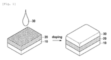
- Fig. 1 is a schematic diagram of explaining an n-doping method of graphene using a doping solution containing an n-type dopant in accordance with an illustrative embodiment of the present disclosure.
- the graphene can be doped by dropping the doping solution containing the n-type dopant on the graphene to form a liquid doping layer.
- the dopant is NaBH 4
- a solvent such as dimethoxyethylether may be used to prepare a doping solution.
- the doping solution is dropped in an amount sufficient to cover the graphene by using surface tension with the graphene and the doping time can be adjusted in a range of from several seconds to several minutes depending on a reducing level of the dopant used.
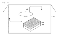
- the graphene can be doped by installing the graphene grown on the substrate in a reaction chamber and supplying the vapor containing the n-type dopant in the reaction chamber.
- the method for doping the graphene using the vapor containing the n-type dopant may include dropping about 3 to 5 drops of an n-type dopant for doping onto tissue paper or gauze and putting it into the sealed reaction chamber together with the graphene. The dopant is vaporized and condensed repeatedly in the sealed reaction chamber to be in a dynamic equilibrium state.
- the above-mentioned method using the vapor containing a dopant is an indirect doping method in which the dopant is not in direct contact with the surface of the graphene, and, thus, it is possible to reduce damage of the graphene to be doped.
- a change in a Dirac point may be measured by manufacturing a Hall bar device so as to check success or failure of doping and a doping level.
- Raman analysis a doping level can be qualitatively measured based on intensity and a shift direction of a peak.
- a 2D-band peak shows a blue shift phenomenon and intensity of the 2D-band peak tends to be weakened.
- n-type doping a 2D-band peak shows a red shift phenomenon and intensity of the 2D-band peak tends to be weakened.
- adsorbates on a surface of the graphene can be sorted by using XPS (X-ray Photoelectron Spectroscopy), and it is possible to check a doping level based on a shift direction and intensity of a C1s peak.
- XPS X-ray Photoelectron Spectroscopy
- graphene used in a doping experiment was grown by a chemical vapor deposition method.
- the grown graphene was transfered onto a SiO 2 /Si substrate, and the graphene was doped by a chemical wet method as illustrated in Fig. 1 .
- As a dopant NaBH 4 dissolved in dimethoxyethylether as a solvent and NH 2 NH 2 (hydrazine) were used.
- the dopant was dropped until the graphene is covered by using surface tension with the graphene and then reacted.
- the NaBH 4 /dimethoxyethylether dopant was used for doping for 2 minutes and the hydrazine dopant was used for doping for 30 seconds.
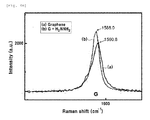
- Figs. 3 and 4 are graphs of Raman spectra for an n-doped graphene in accordance with an example of the present disclosure.
- a G peak commonly found from graphite-based materials is shown at about 1580 cm -1
- a 2D peak is shown at about 2700 cm -1 in graphene.
- a D peak is a peak caused by defects in a crystal and shown around the edge of a graphene specimen, or if there are many defects, the D peak is shown at about 1340 cm -1 .
- Fig. 3 shows Raman spectra obtained from a Raman monochromator after doping with NaBH 4 /dimethoxyethylether in accordance with an example of the present disclosure.
- an intensity ratio of a G peak: a 2D peak varied from about 1:2 to about 1:7, and a 2D peak after doping was red-shifted to an energy region lower than a 2D peak of graphene before doping and intensity was slightly decreased (see Fig. 3C ).
- a G peak became sharp and pointed as intensity was increased after doping.
- a line width of a G peak becomes decreased and intensity becomes further increased. Referring to Fig. 3 in which as a line width of a G peak became decreased, intensity was increased, and as a line width of a 2D peak became decreased, intensity was decreased, it could be seen that graphene was doped. From a fact that the 2D peak was blue-shifted, it could be further confirmed that the graphene was n-doped.
- Fig. 4 shows Raman spectra obtained from a Raman monochromator after doping with hydrazine in accordance with an example of the present disclosure.
- a 2D peak was red-shifted to a low energy region and intensity was decreased.
- a G peak was also red-shifted to a low energy region and intensity was increased. From a fact that a spectrum obtained after doping with hydrazine was similar to the Raman spectrum obtained after doping with the NaBH 4 /dimethoxyethylether, it could be seen that graphene was n-doped with the hydrazine in the same manner as the NaBH 4 /dimethoxyethylether.
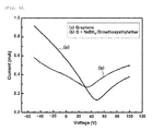
- a Dirac point shift was measured.
- a Dirac point is in a graphene band structure where a valence band and a conduction band are in contact with each other, and a Fermi level of a non-doped graphene becomes equal to the Diract point. Since an electron is shifted to graphene during doping, a Diract point is shifted, which makes it possible to analyze success or failure of doping of graphene.
- a graphene electrode was manufactured as illustrated in Fig. 5 in accordance with an example of the present disclosure.
- a photoresist layer was spin-coated on a graphene, and the photoresist layer was etched by photolithography so as to form an electrode pattern, and then, Cr and Au were deposited in sequence on the etched photoresist layer. Then, after lift-off with acetone, the graphene and the photoresist layer were formed in sequence. Thereafter, the photoresist layer was etched by photolithography, and the graphene at the etched portion was etched by a reactive ion etching method using O 2 plasma. Finally, the remaining photoresist layer was removed.
- a Dirac point when the graphene was doped with NaBH 4 /dimethoxyethylether was lowered by about 20 V as compared with a Dirac point before the doping.
- the positive slope of the graph it could be seen that electron mobility was rarely changed, and referring to the negative slope, the slope after the doping was decreased, and, thus, hole mobility was decreased.
- a Dirac point after the graphene was doped with hydrazine was lowered by about 130 V as compared with a Dirac point before the doping.
- X-ray photoelectron spectroscopy was used as a final method for checking success or failure of doping of graphene.
- various dopants were used, and a change in electron binding energy of a C1s orbital function was monitored.
- As a p-type dopant H 2 SO 4 , HCl, HNO 3 , and AuCl 3 were used, and as an n-type dopant, NaBH 4 /dimethoxyethylether was used, and binding energy was compared.
Landscapes
- Chemical & Material Sciences (AREA)
- Engineering & Computer Science (AREA)
- Nanotechnology (AREA)
- Organic Chemistry (AREA)
- Materials Engineering (AREA)
- Physics & Mathematics (AREA)
- Condensed Matter Physics & Semiconductors (AREA)
- General Physics & Mathematics (AREA)
- Crystallography & Structural Chemistry (AREA)
- Inorganic Chemistry (AREA)
- Composite Materials (AREA)
- Manufacturing & Machinery (AREA)
- Carbon And Carbon Compounds (AREA)
Applications Claiming Priority (2)
| Application Number | Priority Date | Filing Date | Title |
|---|---|---|---|
| KR1020110018425A KR101469450B1 (ko) | 2011-03-02 | 2011-03-02 | 그래핀의 n-도핑 방법 |
| PCT/KR2012/001589 WO2012118350A2 (ko) | 2011-03-02 | 2012-03-02 | 그래핀의 n-도핑 방법 |
Publications (2)
| Publication Number | Publication Date |
|---|---|
| EP2682367A2 true EP2682367A2 (de) | 2014-01-08 |
| EP2682367A4 EP2682367A4 (de) | 2014-10-22 |
Family
ID=46758395
Family Applications (1)
| Application Number | Title | Priority Date | Filing Date |
|---|---|---|---|
| EP12753018.6A Withdrawn EP2682367A4 (de) | 2011-03-02 | 2012-03-02 | Verfahren zur n-dotierung von graphen |
Country Status (6)
| Country | Link |
|---|---|
| US (1) | US20140054550A1 (de) |
| EP (1) | EP2682367A4 (de) |
| JP (1) | JP2014518827A (de) |
| KR (1) | KR101469450B1 (de) |
| CN (1) | CN103502147A (de) |
| WO (1) | WO2012118350A2 (de) |
Cited By (2)
| Publication number | Priority date | Publication date | Assignee | Title |
|---|---|---|---|---|
| EP3015426A1 (de) * | 2014-10-31 | 2016-05-04 | Samsung Electronics Co., Ltd. | Graphenschicht, verfahren zur formung davon, vorrichtung mit der graphenschicht und verfahren zur herstellung der vorrichtung |
| US20220195593A1 (en) * | 2020-12-22 | 2022-06-23 | Jozef Stefan Institute | Method for producing N-doped carbon nanomesh |
Families Citing this family (26)
| Publication number | Priority date | Publication date | Assignee | Title |
|---|---|---|---|---|
| US9202945B2 (en) * | 2011-12-23 | 2015-12-01 | Nokia Technologies Oy | Graphene-based MIM diode and associated methods |
| US9847534B2 (en) * | 2012-04-26 | 2017-12-19 | Indian Institute Of Technology Madras | Metal-alloy graphene nanocomposites and methods for their preparation and use |
| KR101396432B1 (ko) | 2012-08-02 | 2014-05-21 | 경희대학교 산학협력단 | 반도체 소자 및 그의 제조 방법 |
| GB201219417D0 (en) | 2012-10-29 | 2012-12-12 | Univ Ulster | Coatings |
| KR101850112B1 (ko) | 2012-12-26 | 2018-04-19 | 한화테크윈 주식회사 | 그래핀, 그래핀 제조용 조성물 및 이를 이용한 그래핀의 제조 방법 |
| JP6162555B2 (ja) | 2013-09-18 | 2017-07-12 | 株式会社東芝 | 半導体装置、超伝導装置およびその製造方法 |
| KR101842033B1 (ko) | 2014-01-06 | 2018-03-26 | 한화테크윈 주식회사 | 그래핀 제조용 조성물 및 이를 이용한 그래핀의 제조 방법 |
| US10333017B2 (en) | 2014-03-21 | 2019-06-25 | Brookhaven Science Associates, Llc | Hole blocking, electron transporting and window layer for optimized CuIn(1−x)Ga(x)Se2 solar cells |
| CN106148910B (zh) * | 2015-04-03 | 2019-01-04 | 中国科学院上海高等研究院 | 一种氮掺杂石墨烯薄膜的制备方法 |
| CN104817077B (zh) * | 2015-05-07 | 2016-08-24 | 常州大学 | 一种氮磷掺杂石墨烯片的制备方法 |
| CN104817080B (zh) * | 2015-05-07 | 2016-08-17 | 常州大学 | 一种氮硫磷掺杂石墨烯片的制备方法 |
| AU2016316164A1 (en) * | 2015-09-04 | 2018-04-26 | Hiroaki Nakaya | Thermoelectric conversion element and thermoelectric conversion module |
| KR102446411B1 (ko) * | 2015-12-16 | 2022-09-22 | 삼성전자주식회사 | 멀티층 그래핀 및 그 형성방법과 멀티층 그래핀을 포함하는 소자 및 그 제조방법 |
| KR102522012B1 (ko) * | 2015-12-23 | 2023-04-13 | 삼성전자주식회사 | 전도성 소자 및 이를 포함하는 전자 소자 |
| US10106417B2 (en) | 2015-12-30 | 2018-10-23 | Korea Advanced Institute Of Science And Technology | Method of manufacturing graphene using doped carbon materials |
| EP3187473B1 (de) * | 2016-01-04 | 2018-06-20 | Samsung Electronics Co., Ltd | Elektrische leiter auf graphen-basis und dessen herstellung |
| CN108698829B (zh) * | 2016-03-09 | 2022-06-03 | 东丽株式会社 | 表面处理石墨烯、表面处理石墨烯/有机溶剂分散液、表面处理石墨烯-电极活性物质复合体粒子及电极糊 |
| US10730752B2 (en) | 2016-05-03 | 2020-08-04 | Virginia Commonwealth University | Heteroatom-doped porous carbons for clean energy applications and methods for their synthesis |
| KR102642749B1 (ko) * | 2016-09-07 | 2024-03-04 | 엘지전자 주식회사 | 다중 도핑된 그래핀 및 그 제조방법 |
| KR102025364B1 (ko) * | 2017-01-19 | 2019-09-25 | 한화에어로스페이스 주식회사 | 그래핀 제조용 조성물 및 이를 이용한 그래핀의 제조 방법 |
| KR101956189B1 (ko) | 2017-03-02 | 2019-03-08 | 광주과학기술원 | 질소 도핑 그래핀의 제조방법 |
| JP2019052083A (ja) * | 2017-09-13 | 2019-04-04 | 東レ株式会社 | グラフェン粉末、グラフェン粉末/有機溶媒分散液、グラフェン−電極活物質複合体粒子および電極ペーストおよび電極 |
| SE541515C2 (en) | 2017-12-22 | 2019-10-22 | Graphensic Ab | Assembling of molecules on a 2D material and an electronic device |
| CN110416289B (zh) * | 2018-04-26 | 2023-04-07 | 国家纳米科学中心 | 一种碳材料二极管及其制备方法 |
| EP4358645A3 (de) * | 2019-03-05 | 2024-06-26 | Kabushiki Kaisha Toshiba | Graphenhaltiger film, herstellungsverfahren dafür, graphenhaltiges filmlaminat und fotoelektrisches umwandlungselement |
| KR102852289B1 (ko) * | 2020-01-06 | 2025-08-28 | 삼성전자주식회사 | 그래핀 구조체 및 그 형성 방법 |
Family Cites Families (19)
| Publication number | Priority date | Publication date | Assignee | Title |
|---|---|---|---|---|
| JP3953276B2 (ja) * | 2000-02-04 | 2007-08-08 | 株式会社アルバック | グラファイトナノファイバー、電子放出源及びその作製方法、該電子放出源を有する表示素子、並びにリチウムイオン二次電池 |
| JP3963393B2 (ja) * | 2005-03-01 | 2007-08-22 | インターナショナル・ビジネス・マシーンズ・コーポレーション | カーボンナノチューブ電界効果トランジスタ及びこれの製造方法 |
| WO2008023399A1 (en) * | 2006-08-21 | 2008-02-28 | Fujitsu Limited | n-TYPE SEMICONDUCTOR CARBON NANOTUBES, PROCESS FOR PRODUCTION THEREOF, AND PROCESS FOR PRODUCTION OF SEMICONDUCTOR DEVICES |
| JP4669957B2 (ja) * | 2007-03-02 | 2011-04-13 | 日本電気株式会社 | グラフェンを用いる半導体装置及びその製造方法 |
| JP5186831B2 (ja) * | 2007-08-09 | 2013-04-24 | 富士通株式会社 | グラフェンを用いた電子デバイスの製造方法 |
| US20090174435A1 (en) * | 2007-10-01 | 2009-07-09 | University Of Virginia | Monolithically-Integrated Graphene-Nano-Ribbon (GNR) Devices, Interconnects and Circuits |
| KR101435999B1 (ko) * | 2007-12-07 | 2014-08-29 | 삼성전자주식회사 | 도펀트로 도핑된 산화그라펜의 환원물, 이를 포함하는 박막및 투명전극 |
| JP2009212469A (ja) * | 2008-03-06 | 2009-09-17 | Kaneka Corp | 電解液を蓄電に利用する新規エネルギー貯蔵デバイス |
| KR101634753B1 (ko) * | 2008-11-28 | 2016-06-30 | 삼성전자주식회사 | 탄소나노튜브 엔 도핑 물질 및 이를 이용한 엔 도핑 방법 |
| KR20110134420A (ko) * | 2009-04-01 | 2011-12-14 | 내셔널 유니버시티 코포레이션 홋카이도 유니버시티 | 전계 효과 트랜지스터 |
| KR101423037B1 (ko) * | 2009-07-14 | 2014-08-13 | 그래핀스퀘어 주식회사 | 그래핀 시트의 제조 방법, 그래핀 적층체, 변형 수용성 그래핀 시트의 제조 방법, 변형 수용성 그래핀 시트, 및 이를 이용하는 소자 |
| US8507797B2 (en) * | 2009-08-07 | 2013-08-13 | Guardian Industries Corp. | Large area deposition and doping of graphene, and products including the same |
| SG178258A1 (en) * | 2009-08-07 | 2012-03-29 | Blacklight Power Inc | Heterogeneous hydrogen-catalyst power system |
| KR20110061909A (ko) * | 2009-12-02 | 2011-06-10 | 삼성전자주식회사 | 도펀트로 도핑된 그라펜 및 이를 이용한 소자 |
| CN101717083A (zh) * | 2009-12-29 | 2010-06-02 | 北京大学 | 一种石墨烯及其制备方法 |
| US8278643B2 (en) * | 2010-02-02 | 2012-10-02 | Searete Llc | Doped graphene electronic materials |
| US8709295B2 (en) * | 2010-04-26 | 2014-04-29 | Los Alamos National Security, Llc | Nitrogen-doped carbon-supported cobalt-iron oxygen reduction catalyst |
| US8795434B2 (en) * | 2010-09-01 | 2014-08-05 | Jaw Tian Lin | Method and apparatus for mass production of graphene and carbon tubes by deposition of carbon atoms, on flat surfaces and inside walls of tubes, generated from dissociation of a carbon-containing gas stimulated by a tunable high power pulsed laser |
| US8420042B2 (en) * | 2010-09-21 | 2013-04-16 | High Temperature Physics, Llc | Process for the production of carbon graphenes and other nanomaterials |
-
2011
- 2011-03-02 KR KR1020110018425A patent/KR101469450B1/ko active Active
-
2012
- 2012-03-02 JP JP2013556556A patent/JP2014518827A/ja active Pending
- 2012-03-02 EP EP12753018.6A patent/EP2682367A4/de not_active Withdrawn
- 2012-03-02 WO PCT/KR2012/001589 patent/WO2012118350A2/ko not_active Ceased
- 2012-03-02 CN CN201280020453.XA patent/CN103502147A/zh active Pending
-
2013
- 2013-09-03 US US14/016,665 patent/US20140054550A1/en not_active Abandoned
Cited By (4)
| Publication number | Priority date | Publication date | Assignee | Title |
|---|---|---|---|---|
| EP3015426A1 (de) * | 2014-10-31 | 2016-05-04 | Samsung Electronics Co., Ltd. | Graphenschicht, verfahren zur formung davon, vorrichtung mit der graphenschicht und verfahren zur herstellung der vorrichtung |
| US9660036B2 (en) | 2014-10-31 | 2017-05-23 | Samsung Electronics Co., Ltd. | Graphene layer, method of forming the same, device including graphene layer and method of manufacturing the device |
| US20220195593A1 (en) * | 2020-12-22 | 2022-06-23 | Jozef Stefan Institute | Method for producing N-doped carbon nanomesh |
| US12312679B2 (en) * | 2020-12-22 | 2025-05-27 | Joz̃Stefan Institute | Method for producing N-doped carbon nanomesh |
Also Published As
| Publication number | Publication date |
|---|---|
| WO2012118350A3 (ko) | 2012-10-26 |
| KR20120099910A (ko) | 2012-09-12 |
| KR101469450B1 (ko) | 2014-12-05 |
| CN103502147A (zh) | 2014-01-08 |
| WO2012118350A2 (ko) | 2012-09-07 |
| JP2014518827A (ja) | 2014-08-07 |
| EP2682367A4 (de) | 2014-10-22 |
| US20140054550A1 (en) | 2014-02-27 |
Similar Documents
| Publication | Publication Date | Title |
|---|---|---|
| EP2682367A2 (de) | Verfahren zur n-dotierung von graphen | |
| Sovizi et al. | Plasma processing and treatment of 2D transition metal dichalcogenides: tuning properties and defect engineering | |
| Lin et al. | Bridging the gap between reality and ideal in chemical vapor deposition growth of graphene | |
| Yeh et al. | Single-step growth of graphene and graphene-based nanostructures by plasma-enhanced chemical vapor deposition | |
| Kim et al. | Electrochemical synthesis of CdSe quantum dot array on graphene basal plane using mesoporous silica thin film templates | |
| US8288190B2 (en) | Methods of making heterojunction devices | |
| KR101234180B1 (ko) | 그래핀 필름의 롤투롤 도핑 방법 및 도핑된 그래핀 필름 | |
| Wang et al. | Simultaneous N-intercalation and N-doping of epitaxial graphene on 6H-SiC (0001) through thermal reactions with ammonia | |
| US20130240830A1 (en) | Direct and sequential formation of monolayers of boron nitride and graphene on substrates | |
| US12180584B2 (en) | Method of fabricating hexagonal boron nitride | |
| WO2017196559A1 (en) | Direct formation of hexagonal boron nitride on silicon based dielectrics | |
| EP2994933A1 (de) | Direkte und sequenzielle herstellung von monoschichten aus bornitrid und graphen auf substraten | |
| US20150167148A1 (en) | Method for Synthesis of Uniform Bi-Layer and Few-Layer Hexagonal Boron Nitride Dielectric Films | |
| US10186584B2 (en) | Systems and methods for forming diamond heterojunction junction devices | |
| Kale et al. | Enhanced electron field emission properties of high aspect ratio silicon nanowire–zinc oxide core–shell arrays | |
| Ryu et al. | Gallium dopant-induced tunable electrical properties of reduced graphene oxide using metal organic chemical vapor deposition | |
| De Arco et al. | Large scale graphene by chemical vapor deposition: synthesis, characterization and applications | |
| Dou et al. | The effects of oxygen on controlling the number of carbon layers in the chemical vapor deposition of graphene on a nickel substrate | |
| CN101401190A (zh) | 使用大气压氢等离子体的膜制造方法、精制膜制造方法及装置 | |
| US11823895B2 (en) | Methods and devices for graphene formation on flexible substrates by plasma-enhanced chemical vapor deposition | |
| Sassi | Towards Low Temperature Growth of Tungsten Diselenide and Direct Device Fabrication via Chemical Vapor Deposition | |
| KR20160025332A (ko) | 그래핀을 포함하는 나노와이어 구조체를 기반으로 하는 광전도 소자 및 그 제조 방법 | |
| KR20170032796A (ko) | 방향족 유도체 화합물과 지방족 유도체 화합물을 이용한 그래핀의 제조방법 및 그를 포함하는 전자소자의 제조방법 | |
| Kozhakhmetov | MOCVD Synthesis and Doping of FRONT-END-OF-LINE (FEOL) and BACK-END-OF-LINE (BEOL) Compatible Two-Dimensional WSe2 | |
| Lee et al. | One-pot size-controlled growth of graphene-encapsulated germanium nanocrystals |
Legal Events
| Date | Code | Title | Description |
|---|---|---|---|
| PUAI | Public reference made under article 153(3) epc to a published international application that has entered the european phase |
Free format text: ORIGINAL CODE: 0009012 |
|
| 17P | Request for examination filed |
Effective date: 20130930 |
|
| AK | Designated contracting states |
Kind code of ref document: A2 Designated state(s): AL AT BE BG CH CY CZ DE DK EE ES FI FR GB GR HR HU IE IS IT LI LT LU LV MC MK MT NL NO PL PT RO RS SE SI SK SM TR |
|
| DAX | Request for extension of the european patent (deleted) | ||
| A4 | Supplementary search report drawn up and despatched |
Effective date: 20140919 |
|
| RIC1 | Information provided on ipc code assigned before grant |
Ipc: H01L 21/761 20060101ALI20140915BHEP Ipc: H01L 21/22 20060101ALI20140915BHEP Ipc: H01L 21/329 20060101ALI20140915BHEP Ipc: C01B 31/02 20060101AFI20140915BHEP Ipc: H01L 29/16 20060101ALI20140915BHEP Ipc: C01B 31/04 20060101ALI20140915BHEP Ipc: H01L 21/02 20060101ALI20140915BHEP Ipc: H01L 21/04 20060101ALI20140915BHEP |
|
| 17Q | First examination report despatched |
Effective date: 20150812 |
|
| STAA | Information on the status of an ep patent application or granted ep patent |
Free format text: STATUS: THE APPLICATION IS DEEMED TO BE WITHDRAWN |
|
| 18D | Application deemed to be withdrawn |
Effective date: 20150823 |