EP2682977A2 - Netzelektrodenhaftstruktur, Elektronenemissionsvorrichtung und elektronische Vorrichtung mit dieser Elektronenemissionsvorrichtung - Google Patents
Netzelektrodenhaftstruktur, Elektronenemissionsvorrichtung und elektronische Vorrichtung mit dieser Elektronenemissionsvorrichtung Download PDFInfo
- Publication number
- EP2682977A2 EP2682977A2 EP13169180.0A EP13169180A EP2682977A2 EP 2682977 A2 EP2682977 A2 EP 2682977A2 EP 13169180 A EP13169180 A EP 13169180A EP 2682977 A2 EP2682977 A2 EP 2682977A2
- Authority
- EP
- European Patent Office
- Prior art keywords
- mesh electrode
- electron emission
- adhesion
- mesh
- emission device
- Prior art date
- Legal status (The legal status is an assumption and is not a legal conclusion. Google has not performed a legal analysis and makes no representation as to the accuracy of the status listed.)
- Granted
Links
Images


Classifications
-
- H—ELECTRICITY
- H01—ELECTRIC ELEMENTS
- H01J—ELECTRIC DISCHARGE TUBES OR DISCHARGE LAMPS
- H01J35/00—X-ray tubes
- H01J35/02—Details
-
- H—ELECTRICITY
- H01—ELECTRIC ELEMENTS
- H01J—ELECTRIC DISCHARGE TUBES OR DISCHARGE LAMPS
- H01J19/00—Details of vacuum tubes of the types covered by group H01J21/00
- H01J19/02—Electron-emitting electrodes; Cathodes
- H01J19/24—Cold cathodes, e.g. field-emissive cathode
-
- H—ELECTRICITY
- H01—ELECTRIC ELEMENTS
- H01J—ELECTRIC DISCHARGE TUBES OR DISCHARGE LAMPS
- H01J1/00—Details of electrodes, of magnetic control means, of screens, or of the mounting or spacing thereof, common to two or more basic types of discharge tubes or lamps
- H01J1/02—Main electrodes
-
- H—ELECTRICITY
- H01—ELECTRIC ELEMENTS
- H01J—ELECTRIC DISCHARGE TUBES OR DISCHARGE LAMPS
- H01J1/00—Details of electrodes, of magnetic control means, of screens, or of the mounting or spacing thereof, common to two or more basic types of discharge tubes or lamps
- H01J1/02—Main electrodes
- H01J1/30—Cold cathodes, e.g. field-emissive cathode
-
- H—ELECTRICITY
- H01—ELECTRIC ELEMENTS
- H01J—ELECTRIC DISCHARGE TUBES OR DISCHARGE LAMPS
- H01J3/00—Details of electron-optical or ion-optical arrangements common to two or more basic types of discharge tubes or lamps
- H01J3/02—Electron guns
- H01J3/021—Electron guns using a field emission, photo emission, or secondary emission electron source
-
- H—ELECTRICITY
- H01—ELECTRIC ELEMENTS
- H01J—ELECTRIC DISCHARGE TUBES OR DISCHARGE LAMPS
- H01J31/00—Cathode ray tubes; Electron beam tubes
- H01J31/08—Cathode ray tubes; Electron beam tubes having a screen on or from which an image or pattern is formed, picked up, converted, or stored
- H01J31/10—Image or pattern display tubes, i.e. having electrical input and optical output; Flying-spot tubes for scanning purposes
- H01J31/12—Image or pattern display tubes, i.e. having electrical input and optical output; Flying-spot tubes for scanning purposes with luminescent screen
- H01J31/123—Flat display tubes
- H01J31/125—Flat display tubes provided with control means permitting the electron beam to reach selected parts of the screen, e.g. digital selection
- H01J31/127—Flat display tubes provided with control means permitting the electron beam to reach selected parts of the screen, e.g. digital selection using large area or array sources, i.e. essentially a source for each pixel group
-
- H—ELECTRICITY
- H01—ELECTRIC ELEMENTS
- H01J—ELECTRIC DISCHARGE TUBES OR DISCHARGE LAMPS
- H01J35/00—X-ray tubes
- H01J35/02—Details
- H01J35/04—Electrodes ; Mutual position thereof; Constructional adaptations therefor
- H01J35/06—Cathodes
- H01J35/065—Field emission, photo emission or secondary emission cathodes
-
- H—ELECTRICITY
- H01—ELECTRIC ELEMENTS
- H01J—ELECTRIC DISCHARGE TUBES OR DISCHARGE LAMPS
- H01J63/00—Cathode-ray or electron-stream lamps
- H01J63/02—Details, e.g. electrode, gas filling, shape of vessel
-
- H—ELECTRICITY
- H01—ELECTRIC ELEMENTS
- H01J—ELECTRIC DISCHARGE TUBES OR DISCHARGE LAMPS
- H01J63/00—Cathode-ray or electron-stream lamps
- H01J63/06—Lamps with luminescent screen excited by the ray or stream
-
- H—ELECTRICITY
- H01—ELECTRIC ELEMENTS
- H01J—ELECTRIC DISCHARGE TUBES OR DISCHARGE LAMPS
- H01J9/00—Apparatus or processes specially adapted for the manufacture, installation, removal, maintenance of electric discharge tubes, discharge lamps, or parts thereof; Recovery of material from discharge tubes or lamps
- H01J9/02—Manufacture of electrodes or electrode systems
-
- B—PERFORMING OPERATIONS; TRANSPORTING
- B82—NANOTECHNOLOGY
- B82Y—SPECIFIC USES OR APPLICATIONS OF NANOSTRUCTURES; MEASUREMENT OR ANALYSIS OF NANOSTRUCTURES; MANUFACTURE OR TREATMENT OF NANOSTRUCTURES
- B82Y99/00—Subject matter not provided for in other groups of this subclass
-
- H—ELECTRICITY
- H01—ELECTRIC ELEMENTS
- H01J—ELECTRIC DISCHARGE TUBES OR DISCHARGE LAMPS
- H01J2203/00—Electron or ion optical arrangements common to discharge tubes or lamps
- H01J2203/02—Electron guns
- H01J2203/0204—Electron guns using cold cathodes, e.g. field emission cathodes
- H01J2203/0208—Control electrodes
-
- H—ELECTRICITY
- H01—ELECTRIC ELEMENTS
- H01J—ELECTRIC DISCHARGE TUBES OR DISCHARGE LAMPS
- H01J2235/00—X-ray tubes
- H01J2235/06—Cathode assembly
- H01J2235/062—Cold cathodes
-
- H—ELECTRICITY
- H01—ELECTRIC ELEMENTS
- H01J—ELECTRIC DISCHARGE TUBES OR DISCHARGE LAMPS
- H01J2235/00—X-ray tubes
- H01J2235/06—Cathode assembly
- H01J2235/068—Multi-cathode assembly
-
- H—ELECTRICITY
- H01—ELECTRIC ELEMENTS
- H01J—ELECTRIC DISCHARGE TUBES OR DISCHARGE LAMPS
- H01J2329/00—Electron emission display panels, e.g. field emission display panels
- H01J2329/46—Arrangements of electrodes and associated parts for generating or controlling the electron beams
- H01J2329/4604—Control electrodes
- H01J2329/4608—Gate electrodes
-
- Y—GENERAL TAGGING OF NEW TECHNOLOGICAL DEVELOPMENTS; GENERAL TAGGING OF CROSS-SECTIONAL TECHNOLOGIES SPANNING OVER SEVERAL SECTIONS OF THE IPC; TECHNICAL SUBJECTS COVERED BY FORMER USPC CROSS-REFERENCE ART COLLECTIONS [XRACs] AND DIGESTS
- Y10—TECHNICAL SUBJECTS COVERED BY FORMER USPC
- Y10S—TECHNICAL SUBJECTS COVERED BY FORMER USPC CROSS-REFERENCE ART COLLECTIONS [XRACs] AND DIGESTS
- Y10S977/00—Nanotechnology
- Y10S977/902—Specified use of nanostructure
- Y10S977/932—Specified use of nanostructure for electronic or optoelectronic application
- Y10S977/939—Electron emitter, e.g. spindt emitter tip coated with nanoparticles
Definitions
- a mesh electrode adhesion structure an electron emission device, and an electronic apparatus including the electron emission device, and more particularly, an electron emission device, where adhesion of a mesh electrode is reinforced, and an electronic apparatus including the electron emission device.
- An X-ray generating apparatus having a triode structure, a field emission display, a backlight unit or the like uses an electron emission device including a cathode and a gate electrode.
- an electron emission device including a cathode and a gate electrode.
- a high electric field is required, but the high electric field may adversely affect structural stability between the cathode and the gate electrode inducing a voltage.
- a mesh electrode adhesion structure where a mesh electrode is stably adhered to a substrate, an electron emission device, and an electronic apparatus including the electron emission device.
- a mesh electrode adhesion structure which includes: a substrate, and an opening defined in the substrate; a mesh electrode on the substrate, and a first combination groove defined in the mesh electrode; and an adhesion layer between the substrate and the mesh electrode.
- the mesh electrode includes: a mesh region corresponding to the opening defined in the substrate, and an adhesion region in which the first combination groove exposes the adhesion layer.
- An upper width and a lower width of the first combination groove may be different from each other.
- the upper width may be larger than the lower width.
- An angle between an inner wall of the mesh electrode at the first combination groove and the adhesion layer may be in a range from about 90 degrees (°) to about 130°.
- the first combination groove may be circular or polygonal shaped in a plan view.
- the mesh electrode adhesion structure may further include a second combination groove defined in the adhesion region of the mesh electrode.
- a width of the first combination groove may be different from a width of the second combination groove.
- the adhesion layer may include a protruded portion extending into the first combination groove and combined to an inner wall of the mesh electrode at the first combination groove.
- the adhesion layer may include a glass material.
- the adhesion layer may include glass frit or bulk metal glass.
- the mesh electrode may include a conductive metal, for example, an invar metal.
- an electron emission device which includes: a cathode; an insulation layer on the cathode, and an opening defined in the insulation layer and exposing the cathode; an electron emission source on the cathode and in the opening defined in the insulation layer; a mesh electrode on the insulation layer, and a combination groove defined in the mesh electrode; and an adhesion layer between the insulation layer and the mesh electrode.
- the mesh electrode includes a mesh region corresponding to the opening defined in the insulating layer, and an adhesion region in which the combination groove exposes the adhesion layer.
- the electron emission source may include carbon nanotubes.
- the mesh electrode may further include a plurality of mesh regions, and a first adhesion region between the plurality of mesh regions, in an overall mesh region of the mesh electrode; a second adhesion region outside the overall mesh region; a first combination groove in the first adhesion region, and a second combination groove in the second adhesion region.
- the shapes or sizes of the first combination groove and second combination groove may be different from each other.
- an electron emission device which includes: a cathode; an insulation layer on the cathode, and an opening defined in the insulation layer and exposing the cathode; an electron emission source on the cathode and in the opening defined in the insulation layer; a gate electrode on the insulation layer, and a combination groove defined in the gate electrode; and an adhesion layer between the insulation layer and the gate electrode.
- the gate electrode includes an opening region corresponding to the opening defined in the insulation layer, and an adhesion region in which the combination groove exposes the adhesion layer.
- an electronic apparatus which includes an electron emission device which emits an electron beam; and an anode spaced apart from the electron emission device.
- the anode emits light according to a collision with the electron beam emitted from the electron emission device.
- the electron emission device includes: a cathode; an insulation layer on the cathode, and an opening defined in the insulation layer and exposing the cathode; an electron emission source on the cathode and in the opening defined in the insulation layer; a mesh electrode on the insulation layer, and a combination groove defined in the mesh electrode; and an adhesion layer between the insulation layer and the mesh electrode.
- the mesh electrode includes: a mesh region corresponding to the opening defined in the insulation layer and through which the electron beam is emitted toward the anode, and an adhesion region in which the combination groove exposes the adhesion layer.
- the anode may emit an X-ray
- the electronic apparatus is an X-ray emission apparatus.
- the X-ray emitted from the anode may penetrate a target object, and the electronic apparatus may further include an imaging unit which photographs the X-ray that penetrated through the target object.
- a substrate structure of the electronic apparatus includes the anode, and a fluorescent layer on a surface of the anode, and emits a visible ray.
- the electronic apparatus is a surface light source apparatus which emits the visible ray.
- a substrate structure of the electronic apparatus includes the anode, and a fluorescent layer on a surface of the anode, and emits a visible ray.
- the electronic apparatus is a display apparatus including a pixel array, and the pixel array includes the cathode of the electron emission device independently operating according to pixels of the display apparatus.
- first, second, third, etc. may be used herein to describe various elements, components, regions, layers and/or sections, these elements, components, regions, layers and/or sections should not be limited by these terms. These terms are only used to distinguish one element, component, region, layer or section from another region, layer or section. Thus, a first element, component, region, layer or section discussed below could be termed a second element, component, region, layer or section without departing from the teachings of the invention.
- spatially relative terms such as “below,” “lower,” “under,” “above,” “upper” and the like, may be used herein for ease of description to describe the relationship of one element or feature to another element(s) or feature(s) as illustrated in the figures. It will be understood that the spatially relative terms are intended to encompass different orientations of the device in use or operation, in addition to the orientation depicted in the figures. For example, if the device in the figures is turned over, elements described as “below” or “under” relative to other elements or features would then be oriented “above” relative to the other elements or features. Thus, the exemplary term “below” can encompass both an orientation of above and below. The device may be otherwise oriented (rotated 90 degrees or at other orientations) and the spatially relative descriptors used herein interpreted accordingly.
- Embodiments of the invention are described herein with reference to cross-section illustrations that are schematic illustrations of idealized embodiments (and intermediate structures) of the invention. As such, variations from the shapes of the illustrations as a result, for example, of manufacturing techniques and/or tolerances, are to be expected. Thus, embodiments of the invention should not be construed as limited to the particular shapes of regions illustrated herein but are to include deviations in shapes that result, for example, from manufacturing.
- a high electric field is used, but the high electric field may adversely affect structural stability between the cathode and the gate electrode inducing a voltage.
- a mesh electrode having an electron emission passage in a mesh shape is used as the gate electrode of the electron emission device, and the mesh electrode may adhere to the cathode after being detached from an insulation layer due to the high electric field. Therefore, there remains a need for an improved electrode structure having structural stability with respect to a high electric field used by the electron emission device.
- FIG. 1 is a plan view of an embodiment of an electron emission device 100 according to the present invention
- FIG. 2 is a magnified view of an embodiment of a mesh electrode adhesion structure in region A of the electron emission device 100 of FIG. 1
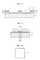
- FIG. 3 is a partial cross-sectional view taken along line I-I of FIG. 2
- FIG. 4 is a partial cross-sectional view taken along line II-II of FIG. 2 .
- the electron emission device 100 includes a cathode 110, an electron emission source 120, an insulation layer 130 and a mesh electrode (or gate electrode) 150.
- the cathode 110 may include a conductive metal, such as an invar metal.
- the electron emission source 120 may include carbon nanotubes, but is not limited thereto or thereby.
- the electron emission source 120 may be on the cathode 110.
- the carbon nanotubes of the electron emission source 120 may be adhered to the cathode 110 such as via a paste method.
- the electron emission source 120 may include a plurality of portions respectively disposed in several regions on a top surface of the cathode 110.
- the insulation layer 130 includes an insulation material and is disposed in a region excluding a region where the electron emission source 120 is disposed, on the top surface of the cathode 110.
- An opening 131 is defined in the insulation layer 130 and corresponding to the region where the electron emission source 120 is disposed.
- a cross-sectional height (e.g., thickness) of the insulation layer 130 is greater higher than a cross-sectional height (e.g., thickness) of the electron emission source 120.
- the heights may be taken perpendicular to the top surface of the cathode 110.
- a total thickness of the electron emission source 120 using the carbon nanotubes may be from about 4 micrometers ( ⁇ m) to about 5 ⁇ m on average, and a thickness of the insulation layer 130 may be about 50 ⁇ m.
- the insulation layer 130 may include a material having insulation characteristics.
- the insulation layer 130 may be formed by patterning a paste having an insulation characteristic, e.g., SiO 2 , on a top surface of the cathode 110 such as via a screen print method.
- the mesh electrode 150 is disposed on a top surface of the insulation layer 130. As shown in FIG. 2 , the mesh electrode 150 may include first and second mesh regions 152 and 153 each including a plurality of electron emission passages 151.
- An electron emission passage 151 may be a discrete pattern, and may have a relatively long, uniform width striped-shape in the plan view.
- the electron emission passages 151 are openings defined in the mesh electrode 150.
- the electron emission passage 151 may be elongated in a first direction, where a width is defined in a second direction perpendicular to the first direction. As illustrated in FIG. 2 , a group of electron emission passages 151 of a mesh region may be arranged in the second direction, but is not limited thereto or thereby.
- Each of the first and second mesh regions 152 and 153 corresponds to or is aligned with a region where the electron emission source 120 is disposed.
- the first mesh region 152 of the mesh electrode 150 corresponds to a region of the openings 131 of the insulation layer 130 indicated by the dotted outline shown in FIG. 2 .
- the opening 131 and the electron emission passage 151 expose the electron emission source 120.
- the opening 131 and the electron emission passage 151 may be aligned, but are not limited thereto or thereby, as long as passage is provide from the electron emission source 120 to outside of the electron emission device 100.
- the mesh electrode 150 may include a conductive metal.
- the mesh electrode 150 may be formed, for example, by patterning an invar metal plate via a laser or spray etch method. Since the openings 131 defined in the insulation layer 130 are located below the first mesh region 152 of the mesh electrode 150, the first mesh region 152 of the mesh electrode 150 may be considered as floating.
- First combination grooves 160 are disposed between the first and second mesh regions 152 and 153 of the mesh electrode 150.
- the first combination grooves 160 may be holes which are defined in and extended through a thickness of the mesh electrode 150. Inner walls of the mesh electrode 150 are exposed at the first combination grooves 160.
- the insulation layer 130 is disposed below a region between the first and second mesh regions 152 and 153 of the mesh electrode 150.
- the region of the mesh electrode 150 between the first and second mesh regions 152 and 153 may be referred to as an adhesion region.
- An adhesion layer 140 may be disposed in the adhesion region, and between the mesh electrode 150 and the insulation layer 130, to adhere the mesh electrode 150 and the insulation layer 130 to each other.
- the first combination groove 160 is in the adhesion region of the mesh electrode 150 between the first and second mesh regions 152 and 153, and exposes the adhesion layer 140 in the adhesion region.
- the adhesion layer 140 may include a glass material, such as glass frit or bulk metal glass, or insulation ceramics, but is not limited thereto or thereby.
- Second combination grooves 170 may be defined in another adhesion region of the mesh electrode 150, and disposed outside an entire or overall mesh region of the mesh electrode 150.
- the overall mesh region may include the first and second mesh regions 152 and 153, and the adhesion region between the first and second mesh regions 152 and 153.
- the second combination grooves 170 may also be holes which are defined in and extended through a thickness of the mesh electrode 150. Inner walls of the mesh electrode 150 are exposed at the second combination grooves 170.
- An area for the first combination grooves 160 may be less than an area for the second combination grooves 170.
- the second combination grooves 170 may be disposed in a wider space than the first combination grooves 160, sizes and shapes of the second combination grooves 170 may not be identical to those of the first combination grooves 160.
- planar sizes or dimensions of the second combination grooves 170 may be larger than those of the first combination grooves 160.
- the first and second combination grooves 160 and 170 have a circular shape in the plan view.
- the planar shapes of the first and second combination grooves 160 and 170 may be different from each other.
- a diameter of the first combination groove 160 may be from about 80 ⁇ m to about 100 ⁇ m, whereas a diameter of the second combination groove 170 may be about 200 ⁇ m.
- one of the first and second combination grooves 160 and 170 may be omitted.
- dimensions at an upper groove area and a lower groove area of the first and second combination grooves 160 and 170 may be different from each other.
- an angle ⁇ between the adhesion layer 140 and each of inner walls of the mesh electrode 150 at the first and second combination grooves 160 and 170 may be from about 90 degrees (°) to about 130°.
- the angle ⁇ between the adhesion layer 140 and the inner wall of the mesh electrode 150 at the second combination groove 170 may be larger than 90° such that an upper diameter D2 of the second combination groove 170 is larger than a lower diameter D1 in the second combination groove 170.
- the combination groove may have an overall truncated conical shape.
- the illustrated embodiment does not eliminate an embodiment where dimensions at the upper groove area and the lower groove area of a combination groove are the same.
- the first and second combination grooves 160 and 170 may have an overall cylindrical shape.
- first and second combination grooves 160 and 170 are not limited to the cylindrical or truncated conical shapes. As illustrated in FIG. 2 , the first and second combination grooves 160 and 170 have a circular shape in the plan view. According to alternative embodiments, the first and second combination grooves 160 and 170 may have a quadrangular shape 161 as shown in FIG. 5A , a hexagonal shape 162 as shown in FIG. 5B , any other polygonal shapes or oval shapes, in the plan view. Dimensions at the upper groove area and the lower groove area of a combination groove having these planar shapes may be different from each other or may be the same as each other, as described above.
- the first and second combination grooves 160 and 170 of the mesh electrode 150 reinforce adhesion between the mesh electrode 150 and the adhesion layer 140, such that the mesh electrode 150 is stably adhered to the insulation layer 130 via the adhesion layer 140.
- some of the adhesion layer 140 e.g., including a glass material rises along the inner walls of the mesh electrode 150 at the first and second combination grooves 160 and 170, thereby reinforcing the adhesion between the mesh electrode 150 and the adhesion layer 140.
- the mesh electrode 150 when the mesh electrode 150 is adhered to the insulation layer 130, e.g., a substrate, in the illustrated embodiment, not only is a surface-surface adhesion between the mesh electrode 150 and the insulation layer 130 obtained by the adhesion layer 140, but a stronger adhesion between the mesh electrode 150 and the insulation layer 130 is also obtained via a geometrical combination of the first and second combination grooves 160 and 170, and the adhesion layer 140.
- the opening 131 defined in the insulation layer 130 is disposed below the first and second mesh regions 152 and 153 of the mesh electrode 150, and thus the first and second mesh regions 152 and 153 float.
- the mesh electrode when a high voltage is applied to a mesh electrode, the mesh electrode may be detached from an underlying insulation layer.
- the adhesion of the mesh electrode 150 to the insulation layer 130 is reinforced by defining the first and second combination grooves 160 and 170 in the mesh electrode 150, and thus the mesh electrode 150 of a mesh type is stably adhered to the insulation layer 130 via the adhesion layer 140.
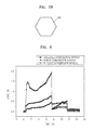
- FIG. 6 is a graph showing results of adhesion measured via a peel test for separating the mesh electrode 150 and the insulation layer 130 of an electron emission from each other after adhering the mesh electrode 150 to the insulation layer 130 to each other by using glass frit (e.g., the adhesion layer 140).
- the adhesion was measured for an embodiment of an electron emission device 100 according to the present invention including combination grooves (e.g., the first and second combination grooves 160 and 170 of FIG.
- an embodiment of an electron emission device 100 according to the present invention including simple combination grooves having the same upper and lower diameters (-- ⁇ --), and a comparative embodiment of an electron emission device not including any combination grooves (-- ⁇ --).
- adhesion of a mesh electrode having the simple combination grooves is 1.64 times higher than that of a mesh electrode without combination grooves. Furthermore, adhesion of a mesh electrode including combination grooves having an upper diameter of 100 ⁇ m and a lower diameter of 50 ⁇ m is 4.24 times higher than that of the mesh electrode without combination grooves. As such, by increasing adhesion between a mesh electrode and an insulation layer, structural stability between the mesh electrode and the cathode may be increased.
- FIG. 7 is a schematic diagram of an embodiment an X-ray emission apparatus 190 employing the electron emission device 100 of FIG. 1 .
- the X-ray emission apparatus 190 includes the electron emission device 100 and an anode 180.
- the electron emission device 100 may be any one of the electron emission devices 100 described above with reference to FIGS. 1 through 6 .
- the anode 180 converts electrons 191 emitted from the electron emission device 100 into an X-ray 195.
- the anode 180 includes a target including of a metal, such as molybdenum (Mo), silver (Ag), tungsten (W), chromium (Cr), iron (Fe), cobalt (Co), or copper (Cu) or a metal alloy thereof.
- the electron emission device 100 and the anode 180 may be each connected to an external power supply unit (not shown).
- the electron emission device 100 and the anode 180 may be provided in a sealed container (not shown) whose inner portion is maintained in a vacuum state.
- the sealed container may include a window through which the X-ray 195 from the inner portion is emitted to an outer portion thereof.
- the sealed container may include stainless steel such that a region excluding the window blocks the X-ray 195.
- FIG. 8 is a graph showing a change in electrical current in milliamps (mA) in an anode according to a driving voltage in volts (V), in the X-ray emission apparatus.
- the change in electrical current is shown for the X-ray emission apparatus 190 including an embodiment of the electron emission device 100 of the present invention (e.g., with combination grooves) (-- ⁇ --), and for an X-ray emission apparatus including a comparative example of an electron emission device without combination grooves (-- ⁇ -- ).
- the X-ray emission apparatus 190 including the electron emission device 100 according to the present invention shows a substantially stable field emission, whereas the X-ray emission apparatus including the comparative example of the electron emission device without combination grooves shows unstable field emission.
- the unstable field emission in the X-ray emission apparatus including the comparative example of the electron emission device may be generated due to a leakage current in a mesh electrode as the mesh electrode is partially detached in the electron emission device not having a combination groove. Accordingly, the X-ray emission apparatus 190 employing the electron emission device 100 of the present invention may emit a more stable X-ray, and thus a more reliable image may be applied when the X-ray emission apparatus 190 is applied to an X-ray imaging apparatus or the like.
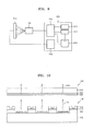
- FIG. 9 is a schematic diagram of an embodiment of an x-ray imaging apparatus 200 employing the X-ray emission apparatus of FIG. 7 .
- the X-ray imaging apparatus 200 include the X-ray emission apparatus 190, a controller 220 controlling the X-ray imaging apparatus 200, an imaging unit 230 photographing an X-ray that is emitted from the X-ray emission apparatus 190 and passed through a target object, an image processor 240 processing image information captured by the imaging unit 230, an input unit 250 into which user manipulation is input, an output unit 270 outputting the processed image information and a data storage unit 280 storing various pieces of information including the image information. Since elements of the X-ray imaging apparatus 200 excluding the X-ray emission apparatus 190 are well known, detailed descriptions thereof are omitted herein.
- FIG. 10 is a diagram of an embodiment of a field emission device (“FED") 300 that is used as a surface light source device, according to the present invention.
- FED field emission device
- the FED 300 includes an electron emission device 100, and a substrate structure.
- the substrate structure includes a transparent substrate 310, and an anode layer 320 and a fluorescent layer 330 on the transparent substrate 310.
- the electron emission device 100 may be any one of the electron emission devices 100 described above with reference to FIGS. 1 through 6 .
- the transparent substrate 310 is disposed to face an electron emitting surface (e.g., a surface where the mesh electrode 150 is disposed) of the electron emission device 100 while being spaced apart from the electron emitting surface at a predetermined interval.
- the fluorescent layer 330 includes a cathode luminescence ("CL") type fluorescent material that is excited by electrons 191 emitted and accelerated from the electron emission device 100, and generates visible light.
- the electrons 191 emitted from the electron emission device 100 collide with the fluorescent layer 330 and turn into a visible ray 350.
- a stacking order of the anode layer 320 and the fluorescent layer 330 may be switched.
- the electron emission device 100 and substrate structure including the transparent substrate 310, the anode layer 320 and the fluorescent layer 330 may have a sealed structure.
- the electron emission device 100 and the substrate structure may be provided in a sealed container (not shown).
- the FED 300 may be used as a surface light source of a backlight unit ("BLU") or lighting apparatus of a display apparatus which is not self-emissive, such as a liquid crystal display (“LCD").
- BLU backlight unit
- LCD liquid crystal display
- the FED 300 may be used as an image display apparatus.
- the cathode 110 of the electron emission device 100 when the cathode 110 of the electron emission device 100 is integrally driven with the FED 300, the FED 300 may operate as a surface light source device.
- a pixel array may include the cathode 110 of the electron emission device 100 and may independently operate according to pixels of the display apparatus, such that the FED 300 may operate as a display apparatus displaying an image.
- a mesh electrode adhesion structure may have reinforced adhesion to a substrate via separate combination grooves defined in the mesh electrode.
- the mesh electrode adhesion structure as a gate electrode of an electron emission device, the gate electrode may be stably adhered to an insulation layer even in a high electric field.
Landscapes
- Engineering & Computer Science (AREA)
- Manufacturing & Machinery (AREA)
- Cold Cathode And The Manufacture (AREA)
- Cathode-Ray Tubes And Fluorescent Screens For Display (AREA)
Applications Claiming Priority (1)
| Application Number | Priority Date | Filing Date | Title |
|---|---|---|---|
| KR1020120074107A KR101917742B1 (ko) | 2012-07-06 | 2012-07-06 | 메쉬 전극 접합 구조체, 전자 방출 소자, 및 전자 방출 소자를 포함하는 전자 장치 |
Publications (3)
| Publication Number | Publication Date |
|---|---|
| EP2682977A2 true EP2682977A2 (de) | 2014-01-08 |
| EP2682977A3 EP2682977A3 (de) | 2015-11-11 |
| EP2682977B1 EP2682977B1 (de) | 2019-04-10 |
Family
ID=48655946
Family Applications (1)
| Application Number | Title | Priority Date | Filing Date |
|---|---|---|---|
| EP13169180.0A Not-in-force EP2682977B1 (de) | 2012-07-06 | 2013-05-24 | Elektronenemissionsvorrichtung mit einer Netzelektrodenhaftstruktur und elektronische Vorrichtung mit dieser Elektronenemissionsvorrichtung |
Country Status (4)
| Country | Link |
|---|---|
| US (1) | US8938049B2 (de) |
| EP (1) | EP2682977B1 (de) |
| KR (1) | KR101917742B1 (de) |
| CN (1) | CN103531422B (de) |
Families Citing this family (5)
| Publication number | Priority date | Publication date | Assignee | Title |
|---|---|---|---|---|
| WO2013184213A2 (en) * | 2012-05-14 | 2013-12-12 | The General Hospital Corporation | A distributed, field emission-based x-ray source for phase contrast imaging |
| EP3105772B1 (de) * | 2014-02-10 | 2018-04-04 | Luxbright AB | Röntgenstrahlvorrichtung |
| CN105374654B (zh) * | 2014-08-25 | 2018-11-06 | 同方威视技术股份有限公司 | 电子源、x射线源、使用了该x射线源的设备 |
| CN111712950B (zh) | 2018-10-30 | 2023-10-03 | 株式会社Lg新能源 | 锂电极以及包含其的锂二次电池 |
| CN109824009B (zh) * | 2019-01-02 | 2020-12-08 | 华中科技大学 | 基于soi工艺的场发射离子中和器芯片的制造方法 |
Family Cites Families (17)
| Publication number | Priority date | Publication date | Assignee | Title |
|---|---|---|---|---|
| US4160310A (en) * | 1976-12-02 | 1979-07-10 | Texas Instruments Incorporated | Metal-dielectric electron beam scanning stack |
| US5955849A (en) * | 1993-11-15 | 1999-09-21 | The United States Of America As Represented By The Secretary Of The Navy | Cold field emitters with thick focusing grids |
| KR20020007495A (ko) | 2000-07-14 | 2002-01-29 | 김순택 | 냉음극을 채용한 전자총 |
| JP2003151456A (ja) * | 2001-11-12 | 2003-05-23 | Sony Corp | 冷陰極電界電子放出表示装置用カソードパネル及び冷陰極電界電子放出表示装置、並びに、冷陰極電界電子放出表示装置用カソードパネルの製造方法 |
| JP2003263965A (ja) * | 2002-03-08 | 2003-09-19 | Mitsubishi Electric Corp | 冷陰極表示装置及び冷陰極表示装置の製造方法 |
| JP2004014222A (ja) * | 2002-06-05 | 2004-01-15 | Mitsubishi Electric Corp | 冷陰極表示装置および冷陰極表示装置の製造方法 |
| KR100571805B1 (ko) | 2003-01-29 | 2006-04-17 | 삼성에스디아이 주식회사 | 전계방출소자와 이를 적용한 표시소자 및 그 제조방법 |
| KR100591242B1 (ko) | 2004-05-04 | 2006-06-19 | 한국전자통신연구원 | 전계 방출 디스플레이 |
| JP2005340133A (ja) * | 2004-05-31 | 2005-12-08 | Sony Corp | カソードパネル処理方法、並びに、冷陰極電界電子放出表示装置及びその製造方法 |
| KR20060037877A (ko) | 2004-10-29 | 2006-05-03 | 삼성에스디아이 주식회사 | 전자방출 표시장치 및 이의 제조방법 |
| KR20060087706A (ko) | 2005-01-31 | 2006-08-03 | 삼성에스디아이 주식회사 | 전자방출 표시장치용 메쉬전극 구조체의 제조방법 |
| KR100660466B1 (ko) * | 2005-02-01 | 2006-12-22 | 남상희 | 에프이디 소자를 이용한 엑스레이 검출기판 |
| KR20060095156A (ko) | 2005-02-28 | 2006-08-31 | 삼성에스디아이 주식회사 | 도전성 메쉬를 구비한 전자방출 표시장치 |
| JP4878311B2 (ja) * | 2006-03-03 | 2012-02-15 | キヤノン株式会社 | マルチx線発生装置 |
| KR101057285B1 (ko) * | 2008-11-07 | 2011-08-16 | 경희대학교 산학협력단 | 엑스레이를 이용한 박막 측정장치 |
| KR20100082048A (ko) * | 2009-01-08 | 2010-07-16 | 삼성에스디아이 주식회사 | 발광 장치 및 이를 구비한 표시 장치 |
| KR20100083555A (ko) * | 2009-01-14 | 2010-07-22 | 삼성에스디아이 주식회사 | 발광 장치 및 이를 구비한 표시 장치 |
-
2012
- 2012-07-06 KR KR1020120074107A patent/KR101917742B1/ko active Active
-
2013
- 2013-05-14 US US13/893,519 patent/US8938049B2/en active Active
- 2013-05-20 CN CN201310187294.9A patent/CN103531422B/zh not_active Expired - Fee Related
- 2013-05-24 EP EP13169180.0A patent/EP2682977B1/de not_active Not-in-force
Non-Patent Citations (1)
| Title |
|---|
| None |
Also Published As
| Publication number | Publication date |
|---|---|
| US8938049B2 (en) | 2015-01-20 |
| KR101917742B1 (ko) | 2018-11-12 |
| EP2682977B1 (de) | 2019-04-10 |
| KR20140006638A (ko) | 2014-01-16 |
| CN103531422B (zh) | 2017-05-31 |
| CN103531422A (zh) | 2014-01-22 |
| EP2682977A3 (de) | 2015-11-11 |
| US20140010347A1 (en) | 2014-01-09 |
Similar Documents
| Publication | Publication Date | Title |
|---|---|---|
| US8938049B2 (en) | Mesh electrode adhesion structure, electron emission device and electronic apparatus including the electron emission device | |
| US7999453B2 (en) | Electron emitter and a display apparatus utilizing the same | |
| US8004167B2 (en) | Electron emitter and a display apparatus utilizing the same | |
| JP5595854B2 (ja) | 電界放出陰極素子及び電界放出表示装置 | |
| US7504768B2 (en) | Field emission display (FED) and method of manufacture thereof | |
| EP1780744A2 (de) | Elektronenemissionsvorrichtung | |
| WO2002027745A1 (fr) | Source d'electrons a cathode froide et affichage par emission electronique de champ | |
| JP2007035628A (ja) | 電子放出型バックライトユニット、それを備えた平板ディスプレイ装置及びその駆動方法 | |
| JP2005243648A (ja) | 電子放出素子 | |
| US7714493B2 (en) | Field emission device and field emission display employing the same | |
| US7471039B2 (en) | Quadrode field emission display | |
| US7492089B2 (en) | Electron emission type backlight unit and flat panel display device having the same | |
| US7683531B2 (en) | Triode field emission display | |
| CN100576411C (zh) | 电子发射显示器的分隔件及其制造方法 | |
| JP2005063965A (ja) | 電界放出ディスプレイ素子 | |
| US20060158094A1 (en) | Field emission display (FED) | |
| JP4414418B2 (ja) | 電子放出デバイス、およびこれを用いた電子放出表示デバイス | |
| US7102279B2 (en) | FED with insulating supporting device having reflection layer | |
| JP2006324127A (ja) | 平面ディスプレイ | |
| KR100516605B1 (ko) | 전계 방출형 표시소자 | |
| TWI390575B (zh) | 場發射陰極結構及場發射顯示器 | |
| KR20080045016A (ko) | 전자 방출 디바이스, 전자 방출 디바이스의 제조 방법, 및전자 방출 디바이스를 구비한 발광 장치 | |
| JP2006190543A (ja) | 電界放出型光源 | |
| US20060001356A1 (en) | FED including gate-supporting device with gate mask having reflection layer | |
| US20070170837A1 (en) | FED including gate-supporting device with gate mask having reflection layer |
Legal Events
| Date | Code | Title | Description |
|---|---|---|---|
| PUAI | Public reference made under article 153(3) epc to a published international application that has entered the european phase |
Free format text: ORIGINAL CODE: 0009012 |
|
| AK | Designated contracting states |
Kind code of ref document: A2 Designated state(s): AL AT BE BG CH CY CZ DE DK EE ES FI FR GB GR HR HU IE IS IT LI LT LU LV MC MK MT NL NO PL PT RO RS SE SI SK SM TR |
|
| AX | Request for extension of the european patent |
Extension state: BA ME |
|
| PUAL | Search report despatched |
Free format text: ORIGINAL CODE: 0009013 |
|
| AK | Designated contracting states |
Kind code of ref document: A3 Designated state(s): AL AT BE BG CH CY CZ DE DK EE ES FI FR GB GR HR HU IE IS IT LI LT LU LV MC MK MT NL NO PL PT RO RS SE SI SK SM TR |
|
| AX | Request for extension of the european patent |
Extension state: BA ME |
|
| RIC1 | Information provided on ipc code assigned before grant |
Ipc: H01J 35/06 20060101AFI20151008BHEP |
|
| 17P | Request for examination filed |
Effective date: 20160511 |
|
| RBV | Designated contracting states (corrected) |
Designated state(s): AL AT BE BG CH CY CZ DE DK EE ES FI FR GB GR HR HU IE IS IT LI LT LU LV MC MK MT NL NO PL PT RO RS SE SI SK SM TR |
|
| GRAP | Despatch of communication of intention to grant a patent |
Free format text: ORIGINAL CODE: EPIDOSNIGR1 |
|
| STAA | Information on the status of an ep patent application or granted ep patent |
Free format text: STATUS: GRANT OF PATENT IS INTENDED |
|
| INTG | Intention to grant announced |
Effective date: 20181018 |
|
| GRAS | Grant fee paid |
Free format text: ORIGINAL CODE: EPIDOSNIGR3 |
|
| GRAA | (expected) grant |
Free format text: ORIGINAL CODE: 0009210 |
|
| STAA | Information on the status of an ep patent application or granted ep patent |
Free format text: STATUS: THE PATENT HAS BEEN GRANTED |
|
| AK | Designated contracting states |
Kind code of ref document: B1 Designated state(s): AL AT BE BG CH CY CZ DE DK EE ES FI FR GB GR HR HU IE IS IT LI LT LU LV MC MK MT NL NO PL PT RO RS SE SI SK SM TR |
|
| REG | Reference to a national code |
Ref country code: GB Ref legal event code: FG4D |
|
| REG | Reference to a national code |
Ref country code: CH Ref legal event code: EP Ref country code: AT Ref legal event code: REF Ref document number: 1119816 Country of ref document: AT Kind code of ref document: T Effective date: 20190415 |
|
| REG | Reference to a national code |
Ref country code: IE Ref legal event code: FG4D |
|
| REG | Reference to a national code |
Ref country code: DE Ref legal event code: R096 Ref document number: 602013053553 Country of ref document: DE |
|
| REG | Reference to a national code |
Ref country code: NL Ref legal event code: MP Effective date: 20190410 |
|
| REG | Reference to a national code |
Ref country code: LT Ref legal event code: MG4D |
|
| REG | Reference to a national code |
Ref country code: AT Ref legal event code: MK05 Ref document number: 1119816 Country of ref document: AT Kind code of ref document: T Effective date: 20190410 |
|
| PG25 | Lapsed in a contracting state [announced via postgrant information from national office to epo] |
Ref country code: NL Free format text: LAPSE BECAUSE OF FAILURE TO SUBMIT A TRANSLATION OF THE DESCRIPTION OR TO PAY THE FEE WITHIN THE PRESCRIBED TIME-LIMIT Effective date: 20190410 |
|
| PG25 | Lapsed in a contracting state [announced via postgrant information from national office to epo] |
Ref country code: HR Free format text: LAPSE BECAUSE OF FAILURE TO SUBMIT A TRANSLATION OF THE DESCRIPTION OR TO PAY THE FEE WITHIN THE PRESCRIBED TIME-LIMIT Effective date: 20190410 Ref country code: LT Free format text: LAPSE BECAUSE OF FAILURE TO SUBMIT A TRANSLATION OF THE DESCRIPTION OR TO PAY THE FEE WITHIN THE PRESCRIBED TIME-LIMIT Effective date: 20190410 Ref country code: FI Free format text: LAPSE BECAUSE OF FAILURE TO SUBMIT A TRANSLATION OF THE DESCRIPTION OR TO PAY THE FEE WITHIN THE PRESCRIBED TIME-LIMIT Effective date: 20190410 Ref country code: SE Free format text: LAPSE BECAUSE OF FAILURE TO SUBMIT A TRANSLATION OF THE DESCRIPTION OR TO PAY THE FEE WITHIN THE PRESCRIBED TIME-LIMIT Effective date: 20190410 Ref country code: AL Free format text: LAPSE BECAUSE OF FAILURE TO SUBMIT A TRANSLATION OF THE DESCRIPTION OR TO PAY THE FEE WITHIN THE PRESCRIBED TIME-LIMIT Effective date: 20190410 Ref country code: PT Free format text: LAPSE BECAUSE OF FAILURE TO SUBMIT A TRANSLATION OF THE DESCRIPTION OR TO PAY THE FEE WITHIN THE PRESCRIBED TIME-LIMIT Effective date: 20190910 Ref country code: NO Free format text: LAPSE BECAUSE OF FAILURE TO SUBMIT A TRANSLATION OF THE DESCRIPTION OR TO PAY THE FEE WITHIN THE PRESCRIBED TIME-LIMIT Effective date: 20190710 Ref country code: ES Free format text: LAPSE BECAUSE OF FAILURE TO SUBMIT A TRANSLATION OF THE DESCRIPTION OR TO PAY THE FEE WITHIN THE PRESCRIBED TIME-LIMIT Effective date: 20190410 |
|
| PG25 | Lapsed in a contracting state [announced via postgrant information from national office to epo] |
Ref country code: BG Free format text: LAPSE BECAUSE OF FAILURE TO SUBMIT A TRANSLATION OF THE DESCRIPTION OR TO PAY THE FEE WITHIN THE PRESCRIBED TIME-LIMIT Effective date: 20190710 Ref country code: GR Free format text: LAPSE BECAUSE OF FAILURE TO SUBMIT A TRANSLATION OF THE DESCRIPTION OR TO PAY THE FEE WITHIN THE PRESCRIBED TIME-LIMIT Effective date: 20190711 Ref country code: RS Free format text: LAPSE BECAUSE OF FAILURE TO SUBMIT A TRANSLATION OF THE DESCRIPTION OR TO PAY THE FEE WITHIN THE PRESCRIBED TIME-LIMIT Effective date: 20190410 Ref country code: LV Free format text: LAPSE BECAUSE OF FAILURE TO SUBMIT A TRANSLATION OF THE DESCRIPTION OR TO PAY THE FEE WITHIN THE PRESCRIBED TIME-LIMIT Effective date: 20190410 Ref country code: PL Free format text: LAPSE BECAUSE OF FAILURE TO SUBMIT A TRANSLATION OF THE DESCRIPTION OR TO PAY THE FEE WITHIN THE PRESCRIBED TIME-LIMIT Effective date: 20190410 |
|
| REG | Reference to a national code |
Ref country code: CH Ref legal event code: PL |
|
| PG25 | Lapsed in a contracting state [announced via postgrant information from national office to epo] |
Ref country code: AT Free format text: LAPSE BECAUSE OF FAILURE TO SUBMIT A TRANSLATION OF THE DESCRIPTION OR TO PAY THE FEE WITHIN THE PRESCRIBED TIME-LIMIT Effective date: 20190410 Ref country code: IS Free format text: LAPSE BECAUSE OF FAILURE TO SUBMIT A TRANSLATION OF THE DESCRIPTION OR TO PAY THE FEE WITHIN THE PRESCRIBED TIME-LIMIT Effective date: 20190810 |
|
| REG | Reference to a national code |
Ref country code: DE Ref legal event code: R097 Ref document number: 602013053553 Country of ref document: DE |
|
| PG25 | Lapsed in a contracting state [announced via postgrant information from national office to epo] |
Ref country code: EE Free format text: LAPSE BECAUSE OF FAILURE TO SUBMIT A TRANSLATION OF THE DESCRIPTION OR TO PAY THE FEE WITHIN THE PRESCRIBED TIME-LIMIT Effective date: 20190410 Ref country code: CH Free format text: LAPSE BECAUSE OF NON-PAYMENT OF DUE FEES Effective date: 20190531 Ref country code: SK Free format text: LAPSE BECAUSE OF FAILURE TO SUBMIT A TRANSLATION OF THE DESCRIPTION OR TO PAY THE FEE WITHIN THE PRESCRIBED TIME-LIMIT Effective date: 20190410 Ref country code: DK Free format text: LAPSE BECAUSE OF FAILURE TO SUBMIT A TRANSLATION OF THE DESCRIPTION OR TO PAY THE FEE WITHIN THE PRESCRIBED TIME-LIMIT Effective date: 20190410 Ref country code: LI Free format text: LAPSE BECAUSE OF NON-PAYMENT OF DUE FEES Effective date: 20190531 Ref country code: MC Free format text: LAPSE BECAUSE OF FAILURE TO SUBMIT A TRANSLATION OF THE DESCRIPTION OR TO PAY THE FEE WITHIN THE PRESCRIBED TIME-LIMIT Effective date: 20190410 Ref country code: RO Free format text: LAPSE BECAUSE OF FAILURE TO SUBMIT A TRANSLATION OF THE DESCRIPTION OR TO PAY THE FEE WITHIN THE PRESCRIBED TIME-LIMIT Effective date: 20190410 Ref country code: CZ Free format text: LAPSE BECAUSE OF FAILURE TO SUBMIT A TRANSLATION OF THE DESCRIPTION OR TO PAY THE FEE WITHIN THE PRESCRIBED TIME-LIMIT Effective date: 20190410 |
|
| REG | Reference to a national code |
Ref country code: BE Ref legal event code: MM Effective date: 20190531 |
|
| PLBE | No opposition filed within time limit |
Free format text: ORIGINAL CODE: 0009261 |
|
| STAA | Information on the status of an ep patent application or granted ep patent |
Free format text: STATUS: NO OPPOSITION FILED WITHIN TIME LIMIT |
|
| PG25 | Lapsed in a contracting state [announced via postgrant information from national office to epo] |
Ref country code: SM Free format text: LAPSE BECAUSE OF FAILURE TO SUBMIT A TRANSLATION OF THE DESCRIPTION OR TO PAY THE FEE WITHIN THE PRESCRIBED TIME-LIMIT Effective date: 20190410 Ref country code: LU Free format text: LAPSE BECAUSE OF NON-PAYMENT OF DUE FEES Effective date: 20190524 Ref country code: IT Free format text: LAPSE BECAUSE OF FAILURE TO SUBMIT A TRANSLATION OF THE DESCRIPTION OR TO PAY THE FEE WITHIN THE PRESCRIBED TIME-LIMIT Effective date: 20190410 |
|
| 26N | No opposition filed |
Effective date: 20200113 |
|
| PG25 | Lapsed in a contracting state [announced via postgrant information from national office to epo] |
Ref country code: TR Free format text: LAPSE BECAUSE OF FAILURE TO SUBMIT A TRANSLATION OF THE DESCRIPTION OR TO PAY THE FEE WITHIN THE PRESCRIBED TIME-LIMIT Effective date: 20190410 |
|
| PG25 | Lapsed in a contracting state [announced via postgrant information from national office to epo] |
Ref country code: IE Free format text: LAPSE BECAUSE OF NON-PAYMENT OF DUE FEES Effective date: 20190524 |
|
| PG25 | Lapsed in a contracting state [announced via postgrant information from national office to epo] |
Ref country code: BE Free format text: LAPSE BECAUSE OF NON-PAYMENT OF DUE FEES Effective date: 20190531 Ref country code: SI Free format text: LAPSE BECAUSE OF FAILURE TO SUBMIT A TRANSLATION OF THE DESCRIPTION OR TO PAY THE FEE WITHIN THE PRESCRIBED TIME-LIMIT Effective date: 20190410 |
|
| PG25 | Lapsed in a contracting state [announced via postgrant information from national office to epo] |
Ref country code: CY Free format text: LAPSE BECAUSE OF FAILURE TO SUBMIT A TRANSLATION OF THE DESCRIPTION OR TO PAY THE FEE WITHIN THE PRESCRIBED TIME-LIMIT Effective date: 20190410 |
|
| PG25 | Lapsed in a contracting state [announced via postgrant information from national office to epo] |
Ref country code: MT Free format text: LAPSE BECAUSE OF FAILURE TO SUBMIT A TRANSLATION OF THE DESCRIPTION OR TO PAY THE FEE WITHIN THE PRESCRIBED TIME-LIMIT Effective date: 20190410 Ref country code: HU Free format text: LAPSE BECAUSE OF FAILURE TO SUBMIT A TRANSLATION OF THE DESCRIPTION OR TO PAY THE FEE WITHIN THE PRESCRIBED TIME-LIMIT; INVALID AB INITIO Effective date: 20130524 |
|
| PG25 | Lapsed in a contracting state [announced via postgrant information from national office to epo] |
Ref country code: MK Free format text: LAPSE BECAUSE OF FAILURE TO SUBMIT A TRANSLATION OF THE DESCRIPTION OR TO PAY THE FEE WITHIN THE PRESCRIBED TIME-LIMIT Effective date: 20190410 |
|
| PGFP | Annual fee paid to national office [announced via postgrant information from national office to epo] |
Ref country code: GB Payment date: 20220420 Year of fee payment: 10 Ref country code: FR Payment date: 20220425 Year of fee payment: 10 Ref country code: DE Payment date: 20220420 Year of fee payment: 10 |
|
| P01 | Opt-out of the competence of the unified patent court (upc) registered |
Effective date: 20230530 |
|
| REG | Reference to a national code |
Ref country code: DE Ref legal event code: R119 Ref document number: 602013053553 Country of ref document: DE |
|
| GBPC | Gb: european patent ceased through non-payment of renewal fee |
Effective date: 20230524 |
|
| PG25 | Lapsed in a contracting state [announced via postgrant information from national office to epo] |
Ref country code: DE Free format text: LAPSE BECAUSE OF NON-PAYMENT OF DUE FEES Effective date: 20231201 Ref country code: GB Free format text: LAPSE BECAUSE OF NON-PAYMENT OF DUE FEES Effective date: 20230524 |
|
| PG25 | Lapsed in a contracting state [announced via postgrant information from national office to epo] |
Ref country code: FR Free format text: LAPSE BECAUSE OF NON-PAYMENT OF DUE FEES Effective date: 20230531 |