EP2683032B1 - Dispositif comportant une antenne de communication de champ proche alimentée en quadrature - Google Patents
Dispositif comportant une antenne de communication de champ proche alimentée en quadrature Download PDFInfo
- Publication number
- EP2683032B1 EP2683032B1 EP12175229.9A EP12175229A EP2683032B1 EP 2683032 B1 EP2683032 B1 EP 2683032B1 EP 12175229 A EP12175229 A EP 12175229A EP 2683032 B1 EP2683032 B1 EP 2683032B1
- Authority
- EP
- European Patent Office
- Prior art keywords
- nfc antenna
- magnetic field
- antenna
- nfc
- housing
- Prior art date
- Legal status (The legal status is an assumption and is not a legal conclusion. Google has not performed a legal analysis and makes no representation as to the accuracy of the status listed.)
- Active
Links
Images







Classifications
-
- H—ELECTRICITY
- H01—ELECTRIC ELEMENTS
- H01Q—ANTENNAS, i.e. RADIO AERIALS
- H01Q1/00—Details of, or arrangements associated with, antennas
- H01Q1/12—Supports; Mounting means
- H01Q1/22—Supports; Mounting means by structural association with other equipment or articles
- H01Q1/2208—Supports; Mounting means by structural association with other equipment or articles associated with components used in interrogation type services, i.e. in systems for information exchange between an interrogator/reader and a tag/transponder, e.g. in Radio Frequency Identification [RFID] systems
-
- H—ELECTRICITY
- H01—ELECTRIC ELEMENTS
- H01Q—ANTENNAS, i.e. RADIO AERIALS
- H01Q1/00—Details of, or arrangements associated with, antennas
- H01Q1/12—Supports; Mounting means
- H01Q1/22—Supports; Mounting means by structural association with other equipment or articles
- H01Q1/24—Supports; Mounting means by structural association with other equipment or articles with receiving set
- H01Q1/241—Supports; Mounting means by structural association with other equipment or articles with receiving set used in mobile communications, e.g. GSM
- H01Q1/242—Supports; Mounting means by structural association with other equipment or articles with receiving set used in mobile communications, e.g. GSM specially adapted for hand-held use
- H01Q1/243—Supports; Mounting means by structural association with other equipment or articles with receiving set used in mobile communications, e.g. GSM specially adapted for hand-held use with built-in antennas
-
- H—ELECTRICITY
- H01—ELECTRIC ELEMENTS
- H01Q—ANTENNAS, i.e. RADIO AERIALS
- H01Q21/00—Antenna arrays or systems
- H01Q21/28—Combinations of substantially independent non-interacting antenna units or systems
-
- H—ELECTRICITY
- H01—ELECTRIC ELEMENTS
- H01Q—ANTENNAS, i.e. RADIO AERIALS
- H01Q7/00—Loop antennas with a substantially uniform current distribution around the loop and having a directional radiation pattern in a plane perpendicular to the plane of the loop
Definitions
- the specification relates generally to antennas, and specifically to a device having a quadrature near field communication antenna.
- NFC near field communication
- An example of an NFC antenna integrated in a smart phone can be found in EP 2 293 383 A2 .
- a main loop is used together with two secondary loops to minimize transmission in the far field.
- An aspect of the specification provides a device comprising: a housing; a first NFC (near field communication) antenna comprising a coil about parallel to a given side of the housing enabled to produce a first magnetic field that extends from the given side of the housing; a second NFC antenna about parallel with the first NFC antenna, the second NFC antenna comprising at least one respective coil forming two opposing current loops enabled to produce a second magnetic field perpendicular to the first magnetic field; and, a circuit for operating the first NFC antenna and the second NFC antenna in quadrature phase.
- a first NFC near field communication
- the first NFC antenna can comprise a loop antenna.
- the current in the two opposing current loops of the at least one respective coil can flow in opposite directions to produce the second magnetic field.
- the second NFC antenna can comprise a bowtie antenna.
- the second NFC antenna can comprise one or more of a bowtie antenna, a double D coil, a butterfly antenna and a figure eight antenna.
- the second magnetic field can leak from the given side of the housing, about parallel to the given side, when operated by the circuit.
- the device further comprises a magnetic conductor for containing respective portions of the first magnetic field and the second magnetic field internal to the device such that at least a local net portion of the first magnetic field leaks from the given side of the housing perpendicular thereto and at least a respective local net portion of the second magnetic field leaks from the given side of the housing, about parallel to the given side, when operated by the circuit.
- the device can further comprise a processor enabled to: control the circuit; and, one or more of receive and transmit data via the first NFC antenna and the second NFC antenna.
- the first magnetic field and the second magnetic field can form components of a circularly polarized magnetic field.
- the circuit can comprise an LC (inductor-capacitor) quadrature splitter.
- the device can further comprise a transceiver in communication with the first NFC antenna and the second NFC antenna, and the circuit can comprise a phase controlled differential driver of an RF interface of the transceiver.
- the device can further comprise a third NFC antenna about parallel with the first NFC antenna and the second NFC antenna, the third NFC antenna comprising at least two further coils enabled to produce a third magnetic field extending from the housing, perpendicular to the first magnetic field and the second magnetic field.
- the third NFC antenna can partially overlap the second NFC antenna, and can be rotated about 90° thereto to decouple the third NFC antenna from the second NFC antenna.
- Another aspect of the specification provides a method comprising: operating a first NFC (near field communication) antenna to produce a first magnetic field that extends from the given side of a housing of a device, the first NFC antenna comprising a coil about parallel to a given side of the housing; and, operating a second NFC antenna in quadrature phase with the first NFC antenna to produce a second magnetic field perpendicular the first magnetic field, the second NFC antenna about parallel with the first NFC antenna, the second NFC antenna comprising at least one respective coil forming two opposing current loops enabled to produce the second magnetic field.
- NFC near field communication
- the method can further comprise one or more of receiving and transmitting data via the first NFC antenna and the second NFC antenna.
- the method can further comprise: operating a third NFC antenna in quadrature phase with the first NFC antenna to produce a third magnetic field perpendicular the first magnetic field and the second magnetic field, the third NFC antenna comprising at least two further coils enabled to produce the third magnetic field
- a first NFC near field communication
- the computer program product can comprise a non-transitory computer program product.
- the method can further comprise one or more of receiving and transmitting data via the first NFC antenna and the second NFC antenna.
- the method can further comprise: operating a third NFC antenna in quadrature phase with the first NFC antenna to produce a third magnetic field extending from the housing perpendicular the first magnetic field and the second magnetic field, the third NFC antenna comprising at least two further coils enabled to produce the third magnetic field.
- Fig. 1 depicts a schematic diagram of a device 101 comprising a quadrature near field communication (NFC) antenna 103, according to non-limiting implementations.
- Device 101 comprises a housing 109 containing a processor 120 interconnected with a memory 122, a communications interface 124 connected to antenna 103, a display 126, an input device 128, a speaker 132, a microphone 134, a battery 135 and a magnetic conductor 136.
- Quadrature near field communication antenna 103 will be interchangeably referred to hereafter as antenna 103.
- Communications interface 124 will be interchangeably referred to as interface 124.
- antenna 103 comprises a first NFC antenna 143 enabled to produce a first magnetic field, and a second NFC antenna 144 enabled to produce a second magnetic field perpendicular the first magnetic field, second NFC antenna 144 about parallel to first NFC antenna 143.
- interface 124 comprises a circuit 145 enabled to operate first NFC antenna 143 and second NFC antenna 144 in quadrature phase.
- first NFC antenna 143 and second NFC antenna 144 can be arranged such that respective magnetic fields leak from any given side of device 101 including, but not limited to, the rear side, a front side, a top side, a bottom side, a left side or a right side.
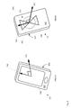
- FIG. 2 depicts front and rear perspective views of device 101; in the rear view of device 101, a relative position of antenna 103 is depicted with respect to a front side 201 and a rear side 202 of housing 109. It is appreciated that antenna 103 is depicted in broken lines in Fig. 2 to indicate that antenna 103 is internal to device 101 and contained within housing 109.
- first NFC antenna 143 comprises a coil about parallel to rear side 202 of housing 109, and hence antenna 143 is enabled to produce a first magnetic field 243 that extends from rear side of housing 109, as best seen in the rear perspective view of device 101.
- First NFC antenna 143 will be explained in more detail with respect to Fig. 3 .
- second NFC antenna 144 comprises at least one respective coil forming two opposing current loops about parallel to rear side 202 of housing 109 enabled to produce a second magnetic field 244 perpendicular to first magnetic field 243, extending along rear side 202 towards a top edge of rear side 202.
- second NFC antenna 144 comprises a bowtie coil, and hence each of the two opposing current loops are formed by a coil having a double-triangle structure as will be explained in more detail with respect to Fig. 4 .
- first magnetic field 243 and second magnetic field 244 are shown in broken lines to indicate they are located behind device 101.
- a front side comprises a side where display 126 is provided; a rear side comprises a side about parallel and opposite to the front side; a left side comprises a side to the left of the front side when display 126 is being viewed, and joining the front side to the rear side; a right side comprises a side to the right of the front side when display 126 is being viewed, and joining the front side to the rear side; a top side comprises a side above the front side when display 126 is being viewed, and joining the front side to the rear side; and a rear side comprises a side below the front side when display 126 is being viewed, and joining the front side to the rear side.
- bottom side, top side, left side and right side generally comprise the depth of device 101 and/or housing 109. Edges can be similarly referred to.
- device 101 can be any type of electronic device that can be used in a self-contained manner to communicate using antenna 103.
- Device 101 includes, but is not limited to, any suitable combination of electronic devices, communications devices, computing devices, personal computers, laptop computers, portable electronic devices, mobile computing devices, portable computing devices, tablet computing devices, laptop computing devices, desktop phones, telephones, PDAs (personal digital assistants), cellphones, smartphones, e-readers, internet-enabled appliances, payment devices, portable speakers, portable headsets and the like. Other suitable devices are within the scope of present implementations.
- device 101 can communicate with communication networks.
- device 101 is enabled to interact with NFC devices, including but not limited to NFC readers, NFC tags and the like, via antenna 103.
- device 101 comprises an NFC devices enabled to interact with, and exchange data with, other NFC devices, including but not limited to one or more of NFC readers, NFC tags, and the like.
- Fig. 1 contemplates a device that can be used for both implementing telephony functions and optionally wireless voice (e.g. telephony) and wireless data communications (e.g. email, web browsing, text, and the like).
- Fig. 1 contemplates a device that can be used for implementing NFC functions, as well as any other specialized functions, including, but not limited, to one or more of, telephony, computing, appliance, payment systems, and/or entertainment related functions.
- Device 101 can comprise at least one input device 128 generally enabled to receive input data, and can comprise any suitable combination of input devices, including but not limited to a keyboard, a keypad, a pointing device, a mouse, a track wheel, a trackball, a touchpad, a touch screen and the like. Other suitable input devices are within the scope of present implementations.
- processor 120 which can be implemented as a plurality of processors, including but not limited to one or more central processors (CPUs)).
- Processor 120 is configured to communicate with a memory 122 comprising a non-volatile storage unit (e.g. Erasable Electronic Programmable Read Only Memory (“EEPROM”), Flash Memory) and a volatile storage unit (e.g. random access memory (“RAM”).
- EEPROM Erasable Electronic Programmable Read Only Memory
- RAM random access memory
- Programming instructions that implement the functional teachings of device 101 as described herein are typically maintained, persistently, in memory 122 and used by processor 120 which makes appropriate utilization of volatile storage during the execution of such programming instructions.
- memory 122 is an example of computer readable media that can store programming instructions executable on processor 120.
- memory 122 is also an example of a memory unit and/or memory module.
- Processor 120 can be further configured to communicate with display 126, and microphone 134 and speaker 132.
- Display 126 comprises any suitable one of, or combination of, CRT (cathode ray tube) and/or flat panel displays (e.g. LCD (liquid crystal display), plasma, OLED (organic light emitting diode), capacitive or resistive touchscreens, and the like).
- Microphone 134 comprises any suitable microphone for receiving sound data.
- Speaker 132 comprises any suitable speaker for providing sound data, audible alerts, audible communications from remote communication devices, and the like, at device 101.
- input device 128 and display 126 are external to device 101, with processor 120 in communication with each of input device 128 and display 126 via a suitable connection and/or link.
- Processor 120 also connects to interface 124, which is enabled to communicate with NFC devices via antenna 103.
- interface 124 comprises a circuit for operating antenna 103 in quadrature phase, as will be explained in further detail below.
- interface 124 can be optionally implemented as one or more radios and/or connectors and/or network adaptors, configured to wirelessly communicate with one or more communication networks (not depicted). It will be appreciated that interface 124 can be configured to correspond with network architecture that is used to implement one or more communication links to one or more communication networks, including but not limited to any suitable combination of USB (universal serial bus) cables, serial cables, wireless links, cell-phone links, cellular network links (including but not limited to 2G, 2.5G, 3G, 4G+, UMTS (Universal Mobile Telecommunications System), CDMA (Code division multiple access), WCDMA (Wideband CDMA), FDD (frequency division duplexing), TDD (time division duplexing), TDD-LTE (TDD-Long Term Evolution), TD-SCDMA (Time Division Synchronous Code Division Multiple Access) and the like, wireless data, Bluetooth links, GPS links, satellite positioning, NFC (near field communication) links, WiFi links, WiMax links, packet based links, the
- interface 124 When interface 124 is configured to communicate with one or more communication networks, interface 124 can comprise further appropriate antennas there for (not depicted).
- device 101 comprises battery 135 or any other suitable power source.
- device 101 comprises a magnetic conductor 136, including but not limited to one or more a magnetic permeable material and a ferrite core.
- battery 135 comprises magnetic conductor 136: in other words, in these implementations, battery 135 can comprise, as a non-limiting example, a ferrite core.
- magnetic conductor 136 is arranged relative to NFC antenna 103 for containing a portion of magnetic fields 243 and 244 internal to device 101 such that at least a local net portion of magnetic fields 243 and 244 leak from rear side 202 of housing 109 and about parallel and perpendicular to rear side 202 when operated by circuit 145, as described below with reference to Fig. 5 . It is furthermore appreciated that magnetic conductor 136 is about planar and can comprise a sheet of magnetic permeable material.
- first NFC antenna 143 comprises a coil (e.g. a loop antenna) forming a current loop, with leads 301, 302 (which connect to circuit 145) supplying a current 303.
- first NFC antenna 143 is depicted, in Fig. 3 , as viewed from rear side 202 of device 101, and further that current 303 is supplied from lead 301: hence current 303 takes a counter-clockwise path around first NFC antenna 143 resulting in first magnetic field 243 going out of the page (e.g. using the right hand rule).
- first magnetic field 243 being about perpendicular to, and extending from, rear side 202 of housing 109 as first NFC antenna 143 is about parallel to rear side 202.
- first NFC antenna 143 is depicted as circular, first NFC antenna 143 can be any suitable shape as long as a current loop is formed and first magnetic field 243 is about perpendicular to rear side 202.
- leads 301, 302 are depicted at a bottom side of first NFC antenna 143, in other implementations leads 301, 302 can be at any other position on first NFC antenna 143 as long as a current loop is formed and first magnetic field 243 is about perpendicular to rear side 202.
- first NFC antenna 143 can comprise any suitable number of turns in the coil with leads 301, 302 connected thereto at any suitable position along the turns.
- first NFC antenna 143 need not be perfectly parallel to rear side 202, and hence first magnetic field 243 need not be perfectly perpendicular rear side 202, as long as first magnetic field 243 is about perpendicular to and/or extends from rear side 202.
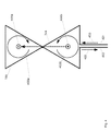
- FIG. 4 depicts second NFC antenna 144 in more detail.
- second NFC antenna 144 comprises a bowtie coil with leads 401, 402 (which connect to circuit 145) supplying a current 403. It is appreciated that second NFC antenna 144 is depicted, in Fig. 4 , as viewed from rear side 202 of device 101, and further that current 403 is supplied from lead 401.
- second NFC antenna 144 hence comprises a coil forming a double triangle structures, which generally form two current loops, 403a, 403b, with current path 403a being clockwise and current path 403b being counter clockwise.
- the double triangle structure is formed by a single coil in a figure 8 shape, but with each of the loops in the figure 8 having a triangle shape.
- the triangles are formed by the coil crossing over in the middle of the double triangle structure (physically crossing but not electrically crossing; in other words, the coil does not short at the cross over point).
- the bottom current loop 403b is formed by current 403 entering second NFC antenna 144 via lead 401, flowing counter clockwise to the cross over point, where clockwise current loop 403a is formed, and then exiting current loop 403a at the cross over point, to again flow counter clockwise to form the remainder of the bottom current loop 403b before exiting via lead 402.
- second NFC antenna comprises at least one coil which forms two opposing current loops.
- a similar structure could be formed without a crossover point by two coils, for example if each of leads 401, 402 were located at about the depicted crossover point, such that each of the top triangle and bottom triangle each formed a continuous loop connected at their apexes (i.e. the current cross over point).
- the structure that forms the two opposing current loops is generally non-limiting and the two opposing current loops can be formed by any suitable number of coils.
- current path 403a results in a net magnetic field 444a going into the page
- current path 403b results in a net magnetic field 444b coming out of the page.
- the near fields of magnetic field 444a and magnetic field 444b generally cancel each other out perpendicular to rear side 202, however as depicted in further detail in Fig. 5 described below, due to the presence of magnetic conductor 136 along one side of second NFC antenna 144, a local net magnetic field results along an opposite side of second NFC antenna 144, that is about perpendicular to net magnetic fields 444a, 444b.
- second magnetic field 244 comprises the local net magnetic field, which hence results in second magnetic field 244 being about perpendicular to first magnetic field 243, as first magnetic field 243 is out of the page, when first NFC antenna 143 is viewed from a similar perspective as second NFC antenna 144 (i.e. the perspectives of each of Figs. 3 and 4 are similar). While not depicted, it is further appreciated that magnetic conductor 136 similarly distorts field lines of magnetic field 243, that result in a net magnetic field about perpendicular to rear side 202.
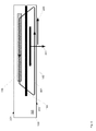
- FIG. 5 depicts a schematic cutaway side view of device 101 showing relative positions of first NFC antenna 143, second NFC antenna 144, and magnetic conductor 136 within housing 109, according to non-limiting implementations. It is appreciated that, in these implementations, first NFC antenna 143 and second NFC antenna 144, are between magnetic conductor 136 and rear side 202, with NFC antenna 143 being the closest to rear side 202. However, second NFC antenna 144 can be closer to rear side 202. Indeed, it is appreciated that the order of first NFC antenna 143 and second NFC antenna 144 is generally non-limiting.
- first NFC antenna 143 and second NFC antenna 144 are generally non-limiting, and that magnetic conductor 136 serves both to distort the magnetic field of first antenna 143 and second antenna 144 and to shield first antenna 143 and second antenna 144 from other electronic, electric fields and magnetic fields generated in device 101. It is further appreciated that a right side of Fig. 5 corresponds to a top side of device 101.
- Fig. 5 also depicts a portion of field lines 501 of second magnetic field 244 flowing through magnetic conductor 136, such that magnetic conductor 136 contains a portion of second magnetic field 244 internal to device 101 such that at least a local net portion of second magnetic field 244, as depicted, leaks from a rear side 202 of housing 109 when operated by circuit 145.
- second magnetic field 244 would be generally symmetrical, though opposite in direction, above and below second NFC antenna 144; but magnetic conductor 136 distorts second magnetic field 244 such that a local net portion of second magnetic field 244 leaks from rear side 202 of device 101, about perpendicular to first magnetic field 243.
- magnetic conductor 136 comprises a sheet of dimensions suitable for distorting second magnetic field 144 as depicted.
- magnetic conductor 136 can be about planar and extending across the complete height and a width of first NFC antenna 143 and second NFC antenna 144.
- magnetic conductor 136 also shields first antenna 143 from other electronics in device 101, and further distorts field lines of first magnetic field 243 such that net first magnetic field 243 leaks from a rear side 202 of device 101 and is about perpendicular to rear side 202.
- magnetic conductor 136 is located such that magnetic fields 243, 244 towards front side 201 are concentrated in magnetic conductor 136 thereby not creating eddy currents with other metal objects at device 101 and leading to a cancelling field: hence, magnetic conductor 136 acts as a shield from metal for first NFC antenna 143 and second NFC antenna 144.
- the structure in Fig. 5 is reversed, with first NFC antenna 143 and second NFC antenna 244 located between front side 201 and magnetic conductor 136.
- the structure in Fig. 5 is adjusted to align with the given side with first NFC antenna 143 and second NFC antenna 244 about parallel to the given side and located between the given side and magnetic conductor 136.
- leads 401, 402 are depicted at a bottom side of second NFC antenna 144, in other implementations leads 401, 402 can be at any other position on second NFC antenna 144 as long as two current loops are formed and second magnetic field 244 is about perpendicular to first magnetic field 243. Further second NFC antenna 144 can comprise any suitable number of turns in the coils with leads 401, 402 connected thereto at any suitable position along the turns.
- second NFC antenna 144 comprises a bowtie antenna.
- second NFC antenna 144 can comprise any suitable antenna comprising at least one respective coil forming two opposing current loops to produce second magnetic field 244.
- second NFC antenna 244 can comprise one or more of a double D antenna 144a, a double D antenna 144b, a figure eight antenna 144c, and an antenna 144d comprising two coils forming current loops in opposite directions.
- second NFC antenna 144 can also comprise a butterfly antenna having any sort of wing shape.
- each of antennas 144a, 144b, 144c, 144d also shows the direction of magnetic fields formed by each of antennas 144a, 144b, 144c, 144d, as well as second magnetic field 244, assuming each antenna 144a, 144b, 144c, 144d is being viewed from rear side 202 of device 101.
- each of the two coils in each of antenna 144b has more turns than antenna 144a; further each of antennas 144a, 144b can comprise any suitable number of turns, which can be co-centric or not co-centric. Similarly, each of the two coils in each of antennas 144, 144a, 144b, 144c, 144d can comprise any suitable number of turns.
- Antennas 144a, 144b further depict leads that are not co-located as with leads 301, 302 and leads 401, 402. Hence, location leads in each of antennas 144, 144a, 144b, 144c, 144d are generally appreciated to be non-limiting.
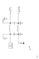
- circuit 145 which comprises an LC (inductor-capacitor) quadrature splitter, with an RF (radio-frequency) interface connected to an RF transceiver as input, and respective lead 301, 401 to first NFC antenna 143 and second NFC antenna 144, which are in quadrature phase to one another. It is appreciated that leads 302, 402 are generally to ground.
- circuit 145 can alternatively comprise a phase controlled differential driver of an RF interface of an RF transceiver of interface 124 driving antennas 143 and 144 differentially.
- Fig, 8 which shows a side schematic view of device 101 and relative positions of first magnetic field 243 and second magnetic field 244 (with a right side of Fig. 8 corresponding to a top of device 101 as first magnetic 243 and second magnetic field 244 are 90° out of phase with one another, they form components of a circularly polarized magnetic field 801 that alternately extend from rear side 202 of device 101 and parallel to rear side 202 of device 101.
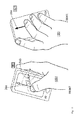
- device 101 can be used detect an NFC device 901 when NFC device 901 is adjacent rear side 202, and/or located towards a top side of device 101 but along rear side 202.
- NFC device 901 when a hand 1001 of a user holding device 101 blocks first magnetic field 243, second magnetic field 244 can be used to detect NFC device 901.
- processor 120 can wirelessly receive, or alternatively transmit, data 903 via first NFC antenna 143 and second NFC antenna 144.
- device 901 can comprise one or more of payment terminal, smart poster tag, inventory terminal and the like.
- FIG. 11 depicts front and rear perspective views of an alternative implementation of a device 101a comprising a quadrature NFC antenna 103a, according to non-limiting implementations.
- Fig. 11 is substantially similar to Fig. 2 , with like elements having like numbers, but with an "a" appended thereto. Further, while an internal schematic of device 101a is not depicted, it is appreciated that device 101a is schematically similar to device 101 as depicted in Fig.
- device 101a comprises a housing 109a containing a processor interconnected with a memory, a communications interface connected to antenna 103a via a circuit, a display, an input device, a speaker , a microphone, a battery and, in some implementations, a magnetic conductor, each respectively similar to housing 109, processor 120, memory 122, interface 124, antenna 103, circuit 145, display 126, input device 128, speaker 132, microphone 134, battery 135 and magnetic conductor 136 as described above.
- First NFC antenna 143a is similar to first NFC antenna 143, and produces a first magnetic field 243a that extends from a rear side 202a of housing 109a, and is about perpendicular to one or more of front side 201a and rear side 202a.
- second NFC antenna 144a is rotated 90° with respect to second NFC antenna 144, such that second magnetic field 244a is perpendicular to first magnetic field 243a but towards a left side or a right side of device 101 a, rather than a top side.
- a left edge, right edge of rear side 202a can be held adjacent the NFC device.
- FIG. 12 depicts front and rear perspective views of an alternative implementation of a device 101b comprising a quadrature NFC antenna 103b, according to non-limiting implementations.
- Fig. 12 is substantially similar to Fig. 2 , with like elements having like numbers, but with a "b" appended thereto. Further, while an internal schematic of device 101b is not depicted, it is appreciated that device 101b is schematically similar to device 101 as depicted in Fig.
- device 101b comprises a housing 109b containing a processor interconnected with a memory, a communications interface connected to antenna 103b via a circuit, a display, an input device, a speaker , a microphone, a battery and, in some implementations, a magnetic conductor, each respectively similar to housing 109, processor 120, memory 122, interface 124, antenna 103, circuit 145, display 126, input device 128, speaker 132, microphone 134, battery 135 and magnetic conductor 136 as described above.
- First NFC antenna 143b is similar to first NFC antenna 143, and produces a first magnetic field 243b that extends from a rear side 202b of housing 109b, and is about perpendicular to one or more of front side 201b and rear side 202b.
- Second NFC antenna 144b is similar to first NFC antenna 144, and produces a second magnetic field 244b perpendicular first magnetic field 243b extending about parallel along rear side 202 towards a top edge of rear side 202.
- device 101b further comprises a third NFC antenna 1244 about parallel with first NFC antenna 143b and second NFC antenna 144b, third NFC antenna 1244 comprising at least two further coils enabled to produce a third magnetic field 1245 extending from housing 109b, perpendicular to first magnetic field 243b and second magnetic field 244b extending about parallel along rear side 202 towards a left edge or a right edge of rear side 202.
- third NFC antenna 1244 is rotated about 90° with respect to second NFC antenna 144b, similar to second NFC antenna 144a of Fig. 11 .
- third NFC antenna 1244 is of a similar type as second NFC antenna 144b: for example, in depicted implementations, both second NFC antenna 144b and third NFC antenna 1244 are bowtie coils.
- second NFC antenna 144b and third NFC antenna 1244 can each be a different type of antenna; for example, second NFC antenna 144b can comprise a bowtie antenna and third NFC antenna 1244 can comprise a double D antenna rotated about 90° to second NFC antenna 144b. Indeed, it is appreciated that second NFC antenna 144b and third NFC antenna 1244 are fed from the same signal feed and are further placed to partially overlap to decouple them.
- two RF coils can be decoupled by overlapping them which enables the magnetic flux of each coil to pass through the other coil in the opposite direction in a non-overlapping area; the area of overlap can be adjusted such that the mutual inductance between the coils is cancelled by the flux through the overlapping area.
- Fig. 12 does not strictly show second antenna 144b and third antenna 1244 overlapping, it is appreciated that they nonetheless overlap to decouple them from each other.
- Fig. 13 depicts a flowchart of a method 1300 for operating a quadrature NFC antenna, according to non-limiting implementations.
- method 1300 is performed using device 101.
- the following discussion of method 1300 will lead to a further understanding of device 101 and its various components.
- device 101 and/or method 1300 can be varied, and need not work exactly as discussed herein in conjunction with each other, and that such variations are within the scope of present implementations.
- method 1300 is implemented in device 101 by processor 120 and/or interface 124 and/or circuit 145. Indeed, method 1300 is one way in which device 101 can be configured. It is to be emphasized, however, that method 1300 need not be performed in the exact sequence as shown, unless otherwise indicated; and likewise various blocks may be performed in parallel rather than in sequence; hence the elements of method 1300 are referred to herein as "blocks" rather than “steps”. It is also to be understood, however, that method 1300 can be implemented on variations of device 101 as well.
- first NFC antenna 143 is operated to produce first magnetic field 243 that extends from rear side 202 of housing 109 of device 101, first NFC antenna 143 comprising a coil about parallel to a rear side 202 of housing 109, as described above with reference to Figs. 1 to 3 .
- second NFC antenna 144 is operated in quadrature phase with first NFC antenna 143 to produce second magnetic field 244 perpendicular first magnetic field 143, second NFC antenna 144 about parallel with first NFC antenna 143, second NFC antenna 144 comprising at least one respective coil forming two opposing current loops enabled to produce second magnetic field 244, as described above with reference to Figs 1 , 2 , and 4 to 7 .
- data 901 is one or more of received and transmitted via first NFC antenna 143 and second NFC antenna 144.
- blocks 1301 and 1303 is generally non-limiting and can be reversed, and/or blocks 1301 and 1303 can occur in parallel. Further, block 1305 can occur in parallel with one or more of blocks 1301 and 1303 and/or between blocks 1301 and 1303.
- method 1300 can comprise a further block where the third NFC antenna is operated in quadrature phase with first NFC antenna 143 to produce a third magnetic field perpendicular first magnetic field 243 and second magnetic field 144, the third NFC antenna comprising at least two further coils enabled to produce the third magnetic field.
- second NFC antenna 144 and third NFC antenna 1244 have been described with respect to respective magnetic fields 244, 1245 extending along a rear side towards top side, a left side and a right side of devices 101, 101b, present implementations are not so limiting.
- second NFC antenna 144 and/or third NFC antenna 1244 can be at any angle relative to longitudinal axes of devices 101, 101b such that respective magnetic fields 244, 1245 extend along the rear side of devices 101, 101b at any corresponding angle.
- magnetic fields 244, 1245 produced by second NFC antenna 144 and/or third NFC antenna 1244 can be at any angle relative a longitudinal axis of either of devices 101, 101b, but about perpendicular to first magnetic field 243.
- first NFC antenna 143 and second NFC antenna 144 can be arranged such that respective magnetic fields 243, 244 leak from any given side of device 101 including, but not limited to, rear side 201, front side 201, a top side, a bottom side, a left side or a right side.
- the device can interact with external NFC devices without a grip on the device being adjusted so as to not be restricted to device alignment. This further extends coverage of the device for interacting with external NFC devices. It is further appreciated that such a device can further be used as a double resonance solution for separate optimization of NFC card readers and NFC card emulation modes: for example, each coil feed line can have a unique shunt capacitor (forming a respective LC tank resonator) to optimize individual antennas for card emulation and reader modes separately.
Landscapes
- Engineering & Computer Science (AREA)
- Computer Networks & Wireless Communication (AREA)
- Near-Field Transmission Systems (AREA)
Claims (13)
- Dispositif (101) comprenant :un boîtier (109) ;une première antenne de communication en champ proche, NFC pour « Near Field Communication », (143) comprenant une bobine sensiblement parallèle à un côté considéré du boîtier (109) et conçue pour produire un premier champ magnétique qui s'étend à partir du côté considéré du boîtier (109) ;une deuxième antenne NFC (144) sensiblement parallèle à la première antenne NFC (143), la deuxième antenne NFC (144) comprenant au moins une bobine respective formant deux boucles de courant opposées conçues pour produire un deuxième champ magnétique, perpendiculaire du premier champ magnétique ;un circuit (145) destiné à faire fonctionner la première antenne NFC (143) et la deuxième antenne NFC (144) en quadrature de phase ; etle dispositif (101) étant caractérisé par :un conducteur magnétique (136) destiné à contenir des parties respectives du premier champ magnétique et du deuxième champ magnétique à l'intérieur du dispositif (101), si bien qu'au moins une partie nette locale du premier champ magnétique s'échappe par le côté considéré du boîtier (109) perpendiculairement à celui-ci et qu'au moins une partie nette locale respective du deuxième champ magnétique s'échappe par le côté considéré du boîtier (109), sensiblement parallèlement au côté considéré, lorsqu'il est commandé par le circuit (145).
- Dispositif (101) selon la revendication 1, dans lequel le courant peut circuler dans des directions opposées dans les deux boucles de courant opposées de ladite au moins une bobine respective afin de produire le deuxième champ magnétique.
- Dispositif (101) selon la revendication 1 ou 2, dans lequel la deuxième antenne NFC (144) consiste en une antenne en noeud papillon.
- Dispositif (101) selon l'une quelconque des revendications précédentes, dans lequel la deuxième antenne NFC (144) comprend une ou plusieurs des antennes suivantes : antenne en noeud papillon, antenne en double D, antenne papillon et antenne en 8.
- Dispositif (101) selon l'une quelconque des revendications précédentes, dans lequel le deuxième champ magnétique s'échappe par le côté considéré du boîtier (109), sensiblement parallèlement au côté considéré, lorsqu'il est commandé par le circuit (145).
- Dispositif (101) selon l'une quelconque des revendications précédentes, comprenant en outre un processeur en mesure de :commander le circuit (145) ; etsoit recevoir, soit émettre des données, ou les deux, via la première antenne NFC (143) et la deuxième antenne NFC (144).
- Dispositif (101) selon l'une quelconque des revendications précédentes, dans lequel le premier champ magnétique et le deuxième champ magnétique constituent des composantes d'un champ magnétique à polarisation circulaire.
- Dispositif (101) selon l'une quelconque des revendications précédentes, dans lequel le circuit (145) comprend un diviseur en quadrature à inducteur et condensateur.
- Dispositif (101) selon l'une quelconque des revendications précédentes, comprenant en outre un émetteur-récepteur (124) en communication avec la première antenne NFC (143) et la deuxième antenne NFC (144), le circuit (145) comprenant un pilote différentiel commandé en phase pour une interface RF de l'émetteur-récepteur (124).
- Dispositif (101) selon l'une quelconque des revendications précédentes, comprenant en outre une troisième antenne NFC (1244) sensiblement parallèle à la première antenne NFC (143) et à la deuxième antenne NFC (144), la troisième antenne NFC (1244) comprenant au moins deux autres bobines conçues pour produire un troisième champ magnétique qui s'étend à partir du boîtier (109), perpendiculairement au premier champ magnétique et au deuxième champ magnétique.
- Dispositif (101) selon la revendication 10, dans lequel la troisième antenne NFC (1244) est partiellement superposée à la deuxième antenne NFC (144) et est pivotée de 90 ° par rapport à celle-ci afin de découpler la troisième antenne NFC (1244) par rapport à la deuxième antenne NFC (144).
- Procédé comprenant les étapes consistant à :faire fonctionner une première antenne de communication en champ proche, NFC pour « Near Field Communication », (143) pour produire un premier champ magnétique qui s'étend à partir d'un côté considéré d'un boîtier (109) d'un dispositif (101), la première antenne NFC (143) comprenant une bobine sensiblement parallèle au côté considéré du boîtier (109) ; etfaire fonctionner une deuxième antenne NFC (144) en quadrature de phase avec la première antenne NFC (143) pour produire un deuxième champ magnétique, perpendiculaire du premier champ magnétique, la première antenne NFC (143) étant sensiblement parallèle à la première antenne NFC (143), la deuxième antenne NFC (144) comprenant au moins une bobine respective formant deux boucles de courant opposées conçues pour produire le deuxième champ magnétique ;dans lequel le procédé est caractérisé par l'étape consistant à :faire fonctionner un conducteur magnétique (136) qui contient des parties respectives du premier champ magnétique et du deuxième champ magnétique à l'intérieur du dispositif (101), si bien qu'au moins une partie nette locale du premier champ magnétique s'échappe par le côté considéré du boîtier (109) perpendiculairement à celui-ci et qu'au moins une partie nette locale respective du deuxième champ magnétique s'échappe par le côté considéré du boîtier (109), sensiblement parallèlement au côté considéré, lorsqu'il fonctionne.
- Procédé selon la revendication 12, comprenant en outre l'étape consistant à :faire fonctionner une troisième antenne NFC (1244) en quadrature de phase avec la première antenne NFC (143) pour produire un troisième champ magnétique perpendiculaire au premier champ magnétique et au deuxième champ magnétique, la troisième antenne NFC (1244) comprenant au moins deux autres bobines conçues pour produire le troisième champ magnétique.
Priority Applications (2)
| Application Number | Priority Date | Filing Date | Title |
|---|---|---|---|
| EP12175229.9A EP2683032B1 (fr) | 2012-07-06 | 2012-07-06 | Dispositif comportant une antenne de communication de champ proche alimentée en quadrature |
| CA2819720A CA2819720C (fr) | 2012-07-06 | 2013-07-02 | Dispositif pourvu d'une antenne de communication en champ proche en quadrature |
Applications Claiming Priority (1)
| Application Number | Priority Date | Filing Date | Title |
|---|---|---|---|
| EP12175229.9A EP2683032B1 (fr) | 2012-07-06 | 2012-07-06 | Dispositif comportant une antenne de communication de champ proche alimentée en quadrature |
Publications (2)
| Publication Number | Publication Date |
|---|---|
| EP2683032A1 EP2683032A1 (fr) | 2014-01-08 |
| EP2683032B1 true EP2683032B1 (fr) | 2015-11-18 |
Family
ID=46507895
Family Applications (1)
| Application Number | Title | Priority Date | Filing Date |
|---|---|---|---|
| EP12175229.9A Active EP2683032B1 (fr) | 2012-07-06 | 2012-07-06 | Dispositif comportant une antenne de communication de champ proche alimentée en quadrature |
Country Status (2)
| Country | Link |
|---|---|
| EP (1) | EP2683032B1 (fr) |
| CA (1) | CA2819720C (fr) |
Families Citing this family (4)
| Publication number | Priority date | Publication date | Assignee | Title |
|---|---|---|---|---|
| US10499225B2 (en) * | 2014-11-13 | 2019-12-03 | BBPOS Limited | System and method for adjusting variable(s) related to near field communications antenna for mobile devices to ensure antenna operation within a defined operating range |
| CN106685485B (zh) * | 2016-12-30 | 2020-08-14 | 宇龙计算机通信科技(深圳)有限公司 | 一种基于近场通信nfc的信号处理方法及装置 |
| CN109361058B (zh) * | 2018-11-30 | 2024-04-02 | 公安部第一研究所 | 一种远距离识读标签的天线 |
| CN121394834A (zh) * | 2024-07-11 | 2026-01-23 | 荣耀终端股份有限公司 | 一种终端天线和电子设备 |
Family Cites Families (4)
| Publication number | Priority date | Publication date | Assignee | Title |
|---|---|---|---|---|
| GB2180123B (en) * | 1984-12-21 | 1989-01-18 | Senezco Limited | Transponder systems |
| JP4803184B2 (ja) * | 2005-11-22 | 2011-10-26 | 株式会社村田製作所 | コイルアンテナおよび携帯電子機器 |
| MX2009013306A (es) * | 2007-06-08 | 2010-02-15 | Checkpoint Systems Inc | Sistema y metodo de deteccion de eas dinamica. |
| US20110050531A1 (en) * | 2009-08-28 | 2011-03-03 | Panasonic Corporation | Antenna unit and communication device using the same |
-
2012
- 2012-07-06 EP EP12175229.9A patent/EP2683032B1/fr active Active
-
2013
- 2013-07-02 CA CA2819720A patent/CA2819720C/fr active Active
Also Published As
| Publication number | Publication date |
|---|---|
| EP2683032A1 (fr) | 2014-01-08 |
| CA2819720C (fr) | 2016-06-07 |
| CA2819720A1 (fr) | 2014-01-06 |
Similar Documents
| Publication | Publication Date | Title |
|---|---|---|
| US9099765B2 (en) | Device having a quadrature near field communication antenna | |
| US11233314B2 (en) | Mobile terminal | |
| US8907859B2 (en) | Edge-emitting antennas for ultra slim wireless mobile devices | |
| US9801006B2 (en) | NFC antenna architecture for mobile communication device with single-piece metal housing | |
| CN109411873B (zh) | 电子装置 | |
| EP3414792B1 (fr) | Couvercle de dispositif faisant office d'antenne du dispositif | |
| KR101604759B1 (ko) | 안테나 어셈블리 및 이를 갖는 이동 단말기 | |
| US9276321B2 (en) | Diagonally-driven antenna system and method | |
| KR20120105867A (ko) | 이동 단말기 | |
| EP2683032B1 (fr) | Dispositif comportant une antenne de communication de champ proche alimentée en quadrature | |
| KR20170029473A (ko) | 안테나 모듈 | |
| EP2685555B1 (fr) | Antenne tribande pour des applications sans fil non cellulaires | |
| KR20130143475A (ko) | 안테나 장치 및 이를 구비하는 이동 단말기 | |
| KR102471872B1 (ko) | 안테나 모듈 및 이를 구비하는 휴대 단말 | |
| US20150084829A1 (en) | Multiple antenna system for a wireless device | |
| KR20160057281A (ko) | 웨어러블 전자 기기에 내장되는 근거리 무선 통신 칩 및 웨어러블 전자 기기 | |
| KR101572022B1 (ko) | 근거리 무선통신 안테나 및 휴대 단말기 | |
| CN115548699B (zh) | 电子设备 | |
| KR20150014278A (ko) | 영차 공진 구조가 결합된 리트랙터블 안테나 | |
| KR20130069125A (ko) | 이동 단말기 | |
| US20260088486A1 (en) | Antenna apparatus and electronic device including the same | |
| KR101832961B1 (ko) | 이동 단말기 | |
| Qian et al. | Wideband shared-aperture orthogonal mode antenna pair for MIMO application | |
| KR20110068114A (ko) | 다중 안테나 시스템 및 이를 구비한 휴대용 단말기 | |
| KR20140004518A (ko) | 안테나 장치 및 이를 구비하는 이동 단말기 |
Legal Events
| Date | Code | Title | Description |
|---|---|---|---|
| PUAI | Public reference made under article 153(3) epc to a published international application that has entered the european phase |
Free format text: ORIGINAL CODE: 0009012 |
|
| 17P | Request for examination filed |
Effective date: 20120706 |
|
| AK | Designated contracting states |
Kind code of ref document: A1 Designated state(s): AL AT BE BG CH CY CZ DE DK EE ES FI FR GB GR HR HU IE IS IT LI LT LU LV MC MK MT NL NO PL PT RO RS SE SI SK SM TR |
|
| AX | Request for extension of the european patent |
Extension state: BA ME |
|
| GRAP | Despatch of communication of intention to grant a patent |
Free format text: ORIGINAL CODE: EPIDOSNIGR1 |
|
| INTG | Intention to grant announced |
Effective date: 20150703 |
|
| RIC1 | Information provided on ipc code assigned before grant |
Ipc: H01Q 21/28 20060101ALN20150622BHEP Ipc: H01Q 7/00 20060101AFI20150622BHEP |
|
| RIN1 | Information on inventor provided before grant (corrected) |
Inventor name: BEHIN, RAYHAN |
|
| GRAS | Grant fee paid |
Free format text: ORIGINAL CODE: EPIDOSNIGR3 |
|
| GRAA | (expected) grant |
Free format text: ORIGINAL CODE: 0009210 |
|
| AK | Designated contracting states |
Kind code of ref document: B1 Designated state(s): AL AT BE BG CH CY CZ DE DK EE ES FI FR GB GR HR HU IE IS IT LI LT LU LV MC MK MT NL NO PL PT RO RS SE SI SK SM TR |
|
| REG | Reference to a national code |
Ref country code: GB Ref legal event code: FG4D |
|
| REG | Reference to a national code |
Ref country code: CH Ref legal event code: EP |
|
| REG | Reference to a national code |
Ref country code: AT Ref legal event code: REF Ref document number: 761961 Country of ref document: AT Kind code of ref document: T Effective date: 20151215 |
|
| REG | Reference to a national code |
Ref country code: IE Ref legal event code: FG4D |
|
| REG | Reference to a national code |
Ref country code: DE Ref legal event code: R096 Ref document number: 602012012302 Country of ref document: DE |
|
| REG | Reference to a national code |
Ref country code: NL Ref legal event code: MP Effective date: 20160218 |
|
| REG | Reference to a national code |
Ref country code: LT Ref legal event code: MG4D |
|
| REG | Reference to a national code |
Ref country code: AT Ref legal event code: MK05 Ref document number: 761961 Country of ref document: AT Kind code of ref document: T Effective date: 20151118 |
|
| PG25 | Lapsed in a contracting state [announced via postgrant information from national office to epo] |
Ref country code: NL Free format text: LAPSE BECAUSE OF FAILURE TO SUBMIT A TRANSLATION OF THE DESCRIPTION OR TO PAY THE FEE WITHIN THE PRESCRIBED TIME-LIMIT Effective date: 20151118 Ref country code: HR Free format text: LAPSE BECAUSE OF FAILURE TO SUBMIT A TRANSLATION OF THE DESCRIPTION OR TO PAY THE FEE WITHIN THE PRESCRIBED TIME-LIMIT Effective date: 20151118 Ref country code: ES Free format text: LAPSE BECAUSE OF FAILURE TO SUBMIT A TRANSLATION OF THE DESCRIPTION OR TO PAY THE FEE WITHIN THE PRESCRIBED TIME-LIMIT Effective date: 20151118 Ref country code: NO Free format text: LAPSE BECAUSE OF FAILURE TO SUBMIT A TRANSLATION OF THE DESCRIPTION OR TO PAY THE FEE WITHIN THE PRESCRIBED TIME-LIMIT Effective date: 20160218 Ref country code: IT Free format text: LAPSE BECAUSE OF FAILURE TO SUBMIT A TRANSLATION OF THE DESCRIPTION OR TO PAY THE FEE WITHIN THE PRESCRIBED TIME-LIMIT Effective date: 20151118 Ref country code: IS Free format text: LAPSE BECAUSE OF FAILURE TO SUBMIT A TRANSLATION OF THE DESCRIPTION OR TO PAY THE FEE WITHIN THE PRESCRIBED TIME-LIMIT Effective date: 20160318 Ref country code: LT Free format text: LAPSE BECAUSE OF FAILURE TO SUBMIT A TRANSLATION OF THE DESCRIPTION OR TO PAY THE FEE WITHIN THE PRESCRIBED TIME-LIMIT Effective date: 20151118 |
|
| PG25 | Lapsed in a contracting state [announced via postgrant information from national office to epo] |
Ref country code: FI Free format text: LAPSE BECAUSE OF FAILURE TO SUBMIT A TRANSLATION OF THE DESCRIPTION OR TO PAY THE FEE WITHIN THE PRESCRIBED TIME-LIMIT Effective date: 20151118 Ref country code: SE Free format text: LAPSE BECAUSE OF FAILURE TO SUBMIT A TRANSLATION OF THE DESCRIPTION OR TO PAY THE FEE WITHIN THE PRESCRIBED TIME-LIMIT Effective date: 20151118 Ref country code: PT Free format text: LAPSE BECAUSE OF FAILURE TO SUBMIT A TRANSLATION OF THE DESCRIPTION OR TO PAY THE FEE WITHIN THE PRESCRIBED TIME-LIMIT Effective date: 20160318 Ref country code: PL Free format text: LAPSE BECAUSE OF FAILURE TO SUBMIT A TRANSLATION OF THE DESCRIPTION OR TO PAY THE FEE WITHIN THE PRESCRIBED TIME-LIMIT Effective date: 20151118 Ref country code: AT Free format text: LAPSE BECAUSE OF FAILURE TO SUBMIT A TRANSLATION OF THE DESCRIPTION OR TO PAY THE FEE WITHIN THE PRESCRIBED TIME-LIMIT Effective date: 20151118 Ref country code: RS Free format text: LAPSE BECAUSE OF FAILURE TO SUBMIT A TRANSLATION OF THE DESCRIPTION OR TO PAY THE FEE WITHIN THE PRESCRIBED TIME-LIMIT Effective date: 20151118 Ref country code: LV Free format text: LAPSE BECAUSE OF FAILURE TO SUBMIT A TRANSLATION OF THE DESCRIPTION OR TO PAY THE FEE WITHIN THE PRESCRIBED TIME-LIMIT Effective date: 20151118 Ref country code: GR Free format text: LAPSE BECAUSE OF FAILURE TO SUBMIT A TRANSLATION OF THE DESCRIPTION OR TO PAY THE FEE WITHIN THE PRESCRIBED TIME-LIMIT Effective date: 20160219 |
|
| REG | Reference to a national code |
Ref country code: FR Ref legal event code: PLFP Year of fee payment: 5 |
|
| PG25 | Lapsed in a contracting state [announced via postgrant information from national office to epo] |
Ref country code: CZ Free format text: LAPSE BECAUSE OF FAILURE TO SUBMIT A TRANSLATION OF THE DESCRIPTION OR TO PAY THE FEE WITHIN THE PRESCRIBED TIME-LIMIT Effective date: 20151118 |
|
| REG | Reference to a national code |
Ref country code: DE Ref legal event code: R097 Ref document number: 602012012302 Country of ref document: DE |
|
| PG25 | Lapsed in a contracting state [announced via postgrant information from national office to epo] |
Ref country code: SM Free format text: LAPSE BECAUSE OF FAILURE TO SUBMIT A TRANSLATION OF THE DESCRIPTION OR TO PAY THE FEE WITHIN THE PRESCRIBED TIME-LIMIT Effective date: 20151118 Ref country code: DK Free format text: LAPSE BECAUSE OF FAILURE TO SUBMIT A TRANSLATION OF THE DESCRIPTION OR TO PAY THE FEE WITHIN THE PRESCRIBED TIME-LIMIT Effective date: 20151118 Ref country code: RO Free format text: LAPSE BECAUSE OF FAILURE TO SUBMIT A TRANSLATION OF THE DESCRIPTION OR TO PAY THE FEE WITHIN THE PRESCRIBED TIME-LIMIT Effective date: 20151118 Ref country code: EE Free format text: LAPSE BECAUSE OF FAILURE TO SUBMIT A TRANSLATION OF THE DESCRIPTION OR TO PAY THE FEE WITHIN THE PRESCRIBED TIME-LIMIT Effective date: 20151118 Ref country code: SK Free format text: LAPSE BECAUSE OF FAILURE TO SUBMIT A TRANSLATION OF THE DESCRIPTION OR TO PAY THE FEE WITHIN THE PRESCRIBED TIME-LIMIT Effective date: 20151118 |
|
| PLBE | No opposition filed within time limit |
Free format text: ORIGINAL CODE: 0009261 |
|
| STAA | Information on the status of an ep patent application or granted ep patent |
Free format text: STATUS: NO OPPOSITION FILED WITHIN TIME LIMIT |
|
| 26N | No opposition filed |
Effective date: 20160819 |
|
| PG25 | Lapsed in a contracting state [announced via postgrant information from national office to epo] |
Ref country code: SI Free format text: LAPSE BECAUSE OF FAILURE TO SUBMIT A TRANSLATION OF THE DESCRIPTION OR TO PAY THE FEE WITHIN THE PRESCRIBED TIME-LIMIT Effective date: 20151118 |
|
| PG25 | Lapsed in a contracting state [announced via postgrant information from national office to epo] |
Ref country code: BE Free format text: LAPSE BECAUSE OF FAILURE TO SUBMIT A TRANSLATION OF THE DESCRIPTION OR TO PAY THE FEE WITHIN THE PRESCRIBED TIME-LIMIT Effective date: 20151118 |
|
| REG | Reference to a national code |
Ref country code: CH Ref legal event code: PL |
|
| PG25 | Lapsed in a contracting state [announced via postgrant information from national office to epo] |
Ref country code: MC Free format text: LAPSE BECAUSE OF FAILURE TO SUBMIT A TRANSLATION OF THE DESCRIPTION OR TO PAY THE FEE WITHIN THE PRESCRIBED TIME-LIMIT Effective date: 20151118 |
|
| PG25 | Lapsed in a contracting state [announced via postgrant information from national office to epo] |
Ref country code: CH Free format text: LAPSE BECAUSE OF NON-PAYMENT OF DUE FEES Effective date: 20160731 Ref country code: LI Free format text: LAPSE BECAUSE OF NON-PAYMENT OF DUE FEES Effective date: 20160731 |
|
| REG | Reference to a national code |
Ref country code: IE Ref legal event code: MM4A |
|
| REG | Reference to a national code |
Ref country code: FR Ref legal event code: PLFP Year of fee payment: 6 |
|
| PG25 | Lapsed in a contracting state [announced via postgrant information from national office to epo] |
Ref country code: IE Free format text: LAPSE BECAUSE OF NON-PAYMENT OF DUE FEES Effective date: 20160706 |
|
| PG25 | Lapsed in a contracting state [announced via postgrant information from national office to epo] |
Ref country code: LU Free format text: LAPSE BECAUSE OF NON-PAYMENT OF DUE FEES Effective date: 20160706 |
|
| PG25 | Lapsed in a contracting state [announced via postgrant information from national office to epo] |
Ref country code: CY Free format text: LAPSE BECAUSE OF FAILURE TO SUBMIT A TRANSLATION OF THE DESCRIPTION OR TO PAY THE FEE WITHIN THE PRESCRIBED TIME-LIMIT Effective date: 20151118 Ref country code: HU Free format text: LAPSE BECAUSE OF FAILURE TO SUBMIT A TRANSLATION OF THE DESCRIPTION OR TO PAY THE FEE WITHIN THE PRESCRIBED TIME-LIMIT; INVALID AB INITIO Effective date: 20120706 |
|
| PG25 | Lapsed in a contracting state [announced via postgrant information from national office to epo] |
Ref country code: MT Free format text: LAPSE BECAUSE OF NON-PAYMENT OF DUE FEES Effective date: 20160731 Ref country code: TR Free format text: LAPSE BECAUSE OF FAILURE TO SUBMIT A TRANSLATION OF THE DESCRIPTION OR TO PAY THE FEE WITHIN THE PRESCRIBED TIME-LIMIT Effective date: 20151118 Ref country code: MK Free format text: LAPSE BECAUSE OF FAILURE TO SUBMIT A TRANSLATION OF THE DESCRIPTION OR TO PAY THE FEE WITHIN THE PRESCRIBED TIME-LIMIT Effective date: 20151118 |
|
| REG | Reference to a national code |
Ref country code: FR Ref legal event code: PLFP Year of fee payment: 7 |
|
| PG25 | Lapsed in a contracting state [announced via postgrant information from national office to epo] |
Ref country code: BG Free format text: LAPSE BECAUSE OF FAILURE TO SUBMIT A TRANSLATION OF THE DESCRIPTION OR TO PAY THE FEE WITHIN THE PRESCRIBED TIME-LIMIT Effective date: 20151118 |
|
| PG25 | Lapsed in a contracting state [announced via postgrant information from national office to epo] |
Ref country code: AL Free format text: LAPSE BECAUSE OF FAILURE TO SUBMIT A TRANSLATION OF THE DESCRIPTION OR TO PAY THE FEE WITHIN THE PRESCRIBED TIME-LIMIT Effective date: 20151118 |
|
| REG | Reference to a national code |
Ref country code: DE Ref legal event code: R082 Ref document number: 602012012302 Country of ref document: DE Ref country code: DE Ref legal event code: R081 Ref document number: 602012012302 Country of ref document: DE Owner name: MALIKIE INNOVATIONS LTD., IE Free format text: FORMER OWNER: BLACKBERRY LIMITED, WATERLOO, ONTARIO, CA |
|
| REG | Reference to a national code |
Ref country code: GB Ref legal event code: 732E Free format text: REGISTERED BETWEEN 20240620 AND 20240627 |
|
| PGFP | Annual fee paid to national office [announced via postgrant information from national office to epo] |
Ref country code: DE Payment date: 20250728 Year of fee payment: 14 |
|
| PGFP | Annual fee paid to national office [announced via postgrant information from national office to epo] |
Ref country code: GB Payment date: 20250722 Year of fee payment: 14 |
|
| PGFP | Annual fee paid to national office [announced via postgrant information from national office to epo] |
Ref country code: FR Payment date: 20250725 Year of fee payment: 14 |