EP2683079A2 - Amplificateur de condensateur commuté complémentaire pour convertisseurs analogique/numérique (A/N) à chevauchement et autres applications - Google Patents
Amplificateur de condensateur commuté complémentaire pour convertisseurs analogique/numérique (A/N) à chevauchement et autres applications Download PDFInfo
- Publication number
- EP2683079A2 EP2683079A2 EP20130003348 EP13003348A EP2683079A2 EP 2683079 A2 EP2683079 A2 EP 2683079A2 EP 20130003348 EP20130003348 EP 20130003348 EP 13003348 A EP13003348 A EP 13003348A EP 2683079 A2 EP2683079 A2 EP 2683079A2
- Authority
- EP
- European Patent Office
- Prior art keywords
- capacitor
- amplifier
- couple
- switch
- switched
- Prior art date
- Legal status (The legal status is an assumption and is not a legal conclusion. Google has not performed a legal analysis and makes no representation as to the accuracy of the status listed.)
- Granted
Links
Images




Classifications
-
- H—ELECTRICITY
- H03—ELECTRONIC CIRCUITRY
- H03F—AMPLIFIERS
- H03F3/00—Amplifiers with only discharge tubes or only semiconductor devices as amplifying elements
- H03F3/005—Amplifiers with only discharge tubes or only semiconductor devices as amplifying elements using switched capacitors, e.g. dynamic amplifiers; using switched capacitors as resistors in differential amplifiers
-
- H—ELECTRICITY
- H03—ELECTRONIC CIRCUITRY
- H03M—CODING; DECODING; CODE CONVERSION IN GENERAL
- H03M1/00—Analogue/digital conversion; Digital/analogue conversion
- H03M1/12—Analogue/digital converters
-
- H—ELECTRICITY
- H03—ELECTRONIC CIRCUITRY
- H03F—AMPLIFIERS
- H03F3/00—Amplifiers with only discharge tubes or only semiconductor devices as amplifying elements
- H03F3/26—Push-pull amplifiers; Phase-splitters therefor
- H03F3/265—Push-pull amplifiers; Phase-splitters therefor with field-effect transistors only
-
- H—ELECTRICITY
- H03—ELECTRONIC CIRCUITRY
- H03F—AMPLIFIERS
- H03F3/00—Amplifiers with only discharge tubes or only semiconductor devices as amplifying elements
- H03F3/30—Single-ended push-pull [SEPP] amplifiers; Phase-splitters therefor
- H03F3/3001—Single-ended push-pull [SEPP] amplifiers; Phase-splitters therefor with field-effect transistors
-
- H—ELECTRICITY
- H03—ELECTRONIC CIRCUITRY
- H03F—AMPLIFIERS
- H03F3/00—Amplifiers with only discharge tubes or only semiconductor devices as amplifying elements
- H03F3/45—Differential amplifiers
- H03F3/45071—Differential amplifiers with semiconductor devices only
- H03F3/45076—Differential amplifiers with semiconductor devices only characterised by the way of implementation of the active amplifying circuit in the differential amplifier
- H03F3/45179—Differential amplifiers with semiconductor devices only characterised by the way of implementation of the active amplifying circuit in the differential amplifier using MOSFET transistors as the active amplifying circuit
-
- H—ELECTRICITY
- H03—ELECTRONIC CIRCUITRY
- H03F—AMPLIFIERS
- H03F3/00—Amplifiers with only discharge tubes or only semiconductor devices as amplifying elements
- H03F3/70—Charge amplifiers
-
- H—ELECTRICITY
- H03—ELECTRONIC CIRCUITRY
- H03F—AMPLIFIERS
- H03F2203/00—Indexing scheme relating to amplifiers with only discharge tubes or only semiconductor devices as amplifying elements covered by H03F3/00
- H03F2203/45—Indexing scheme relating to differential amplifiers
- H03F2203/45551—Indexing scheme relating to differential amplifiers the IC comprising one or more switched capacitors
-
- H—ELECTRICITY
- H03—ELECTRONIC CIRCUITRY
- H03M—CODING; DECODING; CODE CONVERSION IN GENERAL
- H03M1/00—Analogue/digital conversion; Digital/analogue conversion
- H03M1/12—Analogue/digital converters
- H03M1/14—Conversion in steps with each step involving the same or a different conversion means and delivering more than one bit
- H03M1/16—Conversion in steps with each step involving the same or a different conversion means and delivering more than one bit with scale factor modification, i.e. by changing the amplification between the steps
- H03M1/164—Conversion in steps with each step involving the same or a different conversion means and delivering more than one bit with scale factor modification, i.e. by changing the amplification between the steps the steps being performed sequentially in series-connected stages
Definitions
- This application relates generally to amplifiers and, more particularly, to complementary switched capacitor amplifiers.
- ADC pipelined analog-to-digital converter
- MS/s Mega-samples per second
- Typical applications include digital receivers, base stations, digital imaging and video, and ultrasound.
- MDAC multiplying digital-to-analog converter
- the core of the MDAC is constructed using switched capacitor technology formed around a class-A transconductance amplifier.
- the charge transfer from the power supply to the capacitive load of the transconductance amplifier in this conventional MDAC is inherently inefficient because the amplifier draws a constant current, while it delivers on average only a small fraction of this current to the load. This inefficiency negatively effects the power consumption and/or bandwidth of the pipelined ADC.
- a switched-capacitor amplifier for amplifying an input signal comprises:
- the complementary push-pull amplifier comprises a p-type field-effect transistor (PFET) and a n-type field-effect transistor (NFET), wherein both the PFET and the NFET are configured as amplifying elements.
- PFET p-type field-effect transistor
- NFET n-type field-effect transistor
- the first switch and the second switch are configured to be closed while the third switch and the fourth switch are opened.
- the first switch and the second switch are configured to be opened while the third switch and the fourth switch are closed.
- the switched-capacitor amplifier further comprises:
- the switched-capacitor amplifier further comprises a static level-shifting capacitor coupled between the first summing node of the complementary push-pull amplifier and a second summing node of the complementary push-pull amplifier.
- the switched-capacitor amplifier further comprises:
- a converter stage for a pipelined analog-to-digital converter comprises:
- the complementary push-pull amplifier comprises a p-type field-effect transistor (PFET) and a n-type field-effect transistor (NFET), wherein both the PFET and the NFET are configured as amplifying elements.
- PFET p-type field-effect transistor
- NFET n-type field-effect transistor
- the first switch and the second switch are configured to be closed while the third switch and the fourth switch are opened.
- the first switch and the second switch are configured to be opened while the third switch and the fourth switch are closed.
- the converter stage further comprises:
- the converter stage further comprises a static level-shifting capacitor coupled between the first summing node of the complementary push-pull amplifier and a second summing node of the complementary push-pull amplifier.
- the converter stage further comprises:
- a switched-capacitor amplifier for amplifying an input signal comprises:
- the complementary push-pull amplifier comprises a p-type field-effect transistor (PFET) and a n-type field-effect transistor (NFET), wherein both the PFET and the NFET are configured as amplifying elements.
- PFET p-type field-effect transistor
- NFET n-type field-effect transistor
- the switched-capacitor amplifier further comprises:
- the switched-capacitor amplifier further comprises a static level-shifting capacitor coupled between the first summing node of the complementary push-pull amplifier and a second summing node of the complementary push-pull amplifier.
- the switched-capacitor amplifier further comprises:
- a switched-capacitor amplifier for amplifying an input signal comprises:
- FIG. 1 illustrates a block diagram of a pipelined ADC in accordance with embodiments of the present disclosure.
- FIG. 2 illustrates a MDAC
- FIG. 3 illustrates a single-ended MDAC in accordance with embodiments of the present disclosure.
- FIG. 4 illustrates a single-ended MDAC in accordance with embodiments of the present disclosure.
- FIG. 5 illustrates a differential MDAC in accordance with embodiments of the present disclosure.
- FIG. 6 illustrates a differential, unity-gain amplifier in accordance with embodiments of the present disclosure.
- FIG. 7 illustrates a differential, unity-gain amplifier in accordance with embodiments of the present disclosure.
- references in the specification to "one embodiment,” “an embodiment,” “an example embodiment,” etc., indicate that the embodiment described may include a particular feature, structure, or characteristic, but every embodiment may not necessarily include the particular feature, structure, or characteristic. Moreover, such phrases are not necessarily referring to the same embodiment. Further, when a particular feature, structure, or characteristic is described in connection with an embodiment, it is submitted that it is within the knowledge of one skilled in the art to affect such feature, structure, or characteristic in connection with other embodiments whether or not explicitly described.
- FIG. 1 illustrates a conceptual block diagram of a pipelined ADC 100, in accordance with embodiments of the present disclosure.
- pipelined ADC 100 includes four cascaded converter stages 102-108 that sequentially process an analog input signal to convert the analog input signal into a digital output signal.
- An exemplary configuration of a converter stage is shown at the top of FIG. 1 in further detail.
- each converter stage 102-108 samples and holds its analog input using sample and hold circuit 110 and performs a coarse analog-to-digital conversion of its analog input using ADC 112.
- the error of the conversion performed by ADC 112 is computed by converting the output of ADC 112 back into the analog domain using digital-to-analog converter (DAC) 114 and subtracting the output of DAC 114 from the output of sample and hold circuit 114 using subtractor 116.
- the resultant error value output by subtractor 116 referred to as the residue, is then amplified by amplifier 118 and fed to the next converter stage to extract additional bits.
- the final converter stage 108 may contain only an ADC 112 because there is no need to compute any further residue.
- the ADC outputs from each converter stage 102-108 are aligned in time and combined using time aligner 120 to yield the final digital output.
- MDAC multiplying DAC
- the MDAC is typically included in each converter stage of the pipelined ADC and performs the function of sample and hold circuit 110, DAC 114, subtractor 116, and amplifier 118 as described above.
- the performance of this block usually dictates the power efficiency and/or bandwidth of the entire pipelined ADC.
- FIG. 2 illustrates a single-ended version of an MDAC 200 that includes a switched capacitor network 202 and a class-A transconductance amplifier 204.
- the functionality and implementation of DAC 114 has been omitted from FIG. 2 for clarity purposes.
- MDAC 200 operates in two phases: a sampling phase and an amplification phase. At least two non-overlapping clock signals, labeled as ⁇ 1 and ⁇ 2 in FIG. 2 , are used to control switches S1-S6 in switched capacitor network 202 to operate MDAC 200 in these two phases.
- clock signal ⁇ 1 controls switches S1, S2, and S3 to be closed
- clock signal ⁇ 2 controls switches S4, S5, and S6 to be open. Because switches S1, S2, and S3 are closed, the analog input voltage V IN is sampled with respect to common mode voltage V CMN onto both sampling capacitors C F and C S .
- the common mode voltage V CMN is a DC voltage and is used to bias the n-type field effect transistor (NFET) N1 such that N1 provides proper amplification of the signal coupled to its gate (also referred to as the summing node of transconductance amplifier 204).
- the voltage across capacitors C F and C S is substantially equal to V IN - V CMN
- clock signal ⁇ 2 controls switches S4, S5, and S6 to be closed, and clock signal ⁇ 1 controls switches S1, S2, and S3 to be open.
- Capacitor C F becomes a feedback capacitor coupled between the output (labeled as V OUT in FIG. 2 ) and input of transconductance amplifier 118, and capacitor C S samples the DAC output voltage V REF from DAC 114 (not shown). If V REF differs from V IN , charge sharing between capacitors C S and C F occurs during the amplification phase.
- the voltage across capacitor C F is substantially equal to V OUT - V CMN
- the voltage across capacitor C S is substantially equal to V REF - V CMN
- MDAC 200 provides a residue output voltage V OUT that is given by the difference between V IN and V REF with some gain determined by the values of capacitors C S and C F .
- Transconductance amplifier 204 includes n-type field effect transistor (NFET) N1 and p-type field effect transistor (PFET) P1.
- N1 is biased into its saturation region of operation by common mode voltage V CMN as well as by the current provided by P1.
- P1 is biased by voltage V BP to behave as a DC current source.
- Transconductance amplifier 204 is commonly referred to as a single-ended class-A transconductance amplifier because it has a single amplifying element N1 that is biased so that it is always conducting current. As a result, the charge transfer from the power supply V DD to the capacitive load at the output of transconductance amplifier 204 is inherently inefficient because on average only a small fraction of this current goes to the load.
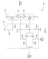
- FIG. 3 illustrates a single-ended MDAC 300 that can provide a higher-level of power efficiency and/or performance in terms of bandwidth than MDAC 200, in accordance with embodiments of the present disclosure.
- MDAC 300 is configured and operates in a similar manner as MDAC 200.
- MDAC 300 includes a complementary push-pull transconductance amplifier 304 and a switched capacitor network 302 with two additional switches S7 and S8 and a level-shifting capacitor C M .
- complementary push-pull transconductance amplifier 304 specifically includes two complementary amplifying elements PFET P1 and NFET N1. This is in contrast to the single amplifying element N1 used in single-ended class-A transconductance amplifier 204.
- PFET P1 and NFET N1 used in single-ended class-A transconductance amplifier 204.
- a larger fraction of the charge from the power supply V DD flowing through complementary push-pull transconductance amplifier 304 can be transferred to the capacitive load at the output of the amplifier compared to single-ended class-A transconductance amplifier 204. This allows MDAC 300 to operate at a higher power efficiency and/or performance level in terms of gain, bandwidth, and speed over MDAC 200.
- Amplifying elements P1 and N1 of complementary push-pull transconductance amplifier 304 can specifically be biased to operate in a class-A, class-B, or class-AB region of operation depending on power and performance demands.
- PFET P2 and NFET N2 of complementary push-pull transconductance amplifier 304 provide a cascode amplifier arrangement.
- P2 and N2 are respectively biased by voltages V BP and V BN .
- the signal to be amplified by complementary push-pull transconductance amplifier 304 is provided to the gates of both P1 and N1 (also referred to as the summing nodes of complementary push-pull transconductance amplifier 304).
- the additional switches S7 and S8 and level-shifting capacitor C M included in switched capacitor network 302 are used to provide both the signal to be amplified and the common mode voltage V CMP to the gate of P1.
- the level-shifting capacitor C M is specifically used to isolate the two DC common mode voltages V CMP and V CMN , while allowing the AC small signal that is to be amplified to pass through to the gate of P1.
- the common mode voltage V CMP is a DC voltage and is used to bias P1 such that P1 provides proper amplification of the signal coupled to its gate.
- switch S7 is controlled by clock signal ⁇ 1 to be closed and switch S8 is controlled by clock signal ⁇ 2 to be open.
- switch S7 is controlled by clock signal ⁇ 1 to be open and switch S8 is controlled by clock signal ⁇ 2 to be closed.
- complementary push-pull transconductance amplifier 304 can use different transistors types (e.g., bipolar junction transistors), configurations (e.g., a non-cascode configuration), and/or additional elements.
- transistors types e.g., bipolar junction transistors
- configurations e.g., a non-cascode configuration
- FIG. 4 illustrates a single-ended MDAC 400 that can provide a higher-level of power efficiency and/or performance in terms of gain, bandwidth, and speed than MDAC 200, in accordance with embodiments of the present disclosure.
- MDAC 400 is configured and operates in a similar manner as MDAC 300.
- MDAC 400 has split level-shifting capacitor C M into two separate level-shifting capacitors: a static level-shifting capacitor C MS and a dynamic level-shifting capacitor C MD .
- Static capacitor C MS remains coupled between the gates of P1 and N1 during both the sampling and amplification phase of operation.
- Dynamic capacitor C MD is charged by common mode voltages V CMP and V CMN during the sampling phase and gradually establishes the desired common mode voltages V CMP and V CMN on the gates of P1 and N1, respectively, during the amplification phase.
- This split cap configuration allows capacitor C MD to be reduced in size compared to C M in MDAC 300, which correspondingly allows the size of switches S7 and S8 to be reduced. For example, where switches S7 and S8 are implemented using pass transistors, the width-to-length ratio of the channels of the pass transistors can be reduced. Moreover, the charge averaging that occurs between capacitors C MS and C MD reduces sampling noise on the two capacitors.
- FIG. 5 illustrates a differential MDAC 500 that can provide a higher-level of power efficiency and/or performance in terms of bandwidth and speed than MDAC 200, in accordance with embodiments of the present disclosure.
- MDAC 500 is configured and operates in a similar manner as MDAC 300.
- MDAC 500 is differential and includes two ends: a first end that includes switched capacitor network 502A and interfaces with a left side of complementary push-pull transconductance amplifier 504, and a second end that includes switched capacitor network 502B and interfaces with a right side of complementary push-pull transconductance amplifier 504.
- the first end of MDAC 500 processes the positive end of the analog input V IN + and the DAC output V REF + to provide the positive end of the residue output signal V OUT +, and the second end of MDAC 500 processes the negative end of the analog input V IN - and the DAC output V REF - to provide the negative end of the residue output signal V OUT -.
- the left and right sides of MDAC 500 are (ideally) symmetrical and include similar elements arranged in the same manner.
- level-shifting capacitors C MA and C MB can be implemented in a similar split configuration as shown in FIG. 4 .
- FIG. 6 illustrates the basic configuration of MDAC 500 illustrated in FIG. 5 in a more generalized form, in accordance with embodiments of the disclosure.
- switched capacitor networks 602A and 602B in FIG. 6 have been modified to omit switches S2A, S2B, S5A, and S5B, and capacitors C MA and C MB .
- the switched capacitor networks 602A and 602B in combination with the complementary push-pull amplifier are configured as a generalized, unity-gain amplifier 600 (or buffer).
- the differential input signal V IN +/- received by unity-gain amplifier 600 undergoes unit gain amplification and is output by unity-gain amplifier via differential output signal V OUT +/-.
- unity-gain amplifier 600 can be modified to include further elements such as resistors, inductors, capacitors, and switches to implement any number of different functions.
- unity-gain amplifier 600 can be modified to include further elements such as resistors, inductors, capacitors, and switches to implement a non-unity gain function.
- unity-gain amplifier 600 can be modified such that level-shifting capacitors C MA and C MB can be implemented in a similar split configuration as shown in FIG. 4 .
- FIG. 7 illustrates a unity-gain amplifier 700 that is a variant of unity-gain amplifier 600, in accordance with embodiments of the present disclosure.
- switched capacitor networks 702A and 702B in FIG. 7 have been modified to omit switches S7A, S7B, S8A, and S8B, and capacitors C MA and C MB , and further include switches S9A, S9B, S10A, and S10B, and capacitors C F2A and C F1A .
- switches S9A and S10A and capacitor C F2A function in the same manner as switches S3A and S6A and capacitor C F1A as described above.
- switches S9B and S10B and capacitor C F2B function in the same manner as switches S3B and S6B and capacitor C F1B as described above.
- unity-gain amplifier 700 can be modified to include further elements such as resistors, inductors, capacitors, and switches to implement any number of different functions.
- unit-gain amplifier 700 can be modified to include further elements such as resistors, inductors, capacitors, and switches to implement a non-unity gain function.
- the differential amplifiers shown in FIGS. 5-7 can further include a tail current source coupled to the sources of the NFET amplifying elements and/or the PFET amplifying elements (i.e., the differential amplifiers shown in FIGS. 5-7 can be implemented as source-coupled pair amplifiers or, as referred to in British literature, long-tailed pair amplifiers).
- a tail current source helps to make the bias currents of both sides of a different amplifier independent of the input common mode level of the amplifier.
- the differential amplifiers shown in FIGS. 6 and 7 can be easily modified to function as single-ended unity gain amplifiers in other implementations. This modification can be as simple as implementing only one of the two symmetrical sides of the differential amplifiers shown in FIGS. 6 and 7 .
- the level-shifting capacitor C MA (or C MB ) in a single-ended version of the unity gain amplifier shown in FIG. 6 can be implemented in a similar split configuration as shown in FIG. 4 .
Landscapes
- Engineering & Computer Science (AREA)
- Power Engineering (AREA)
- Theoretical Computer Science (AREA)
- Amplifiers (AREA)
Priority Applications (1)
| Application Number | Priority Date | Filing Date | Title |
|---|---|---|---|
| EP14004198.9A EP2866346B1 (fr) | 2012-07-06 | 2013-07-02 | Amplificateur de condensateur commuté complémentaire pour convertisseurs analogique/numérique (A/N) à chevauchement et autres applications |
Applications Claiming Priority (1)
| Application Number | Priority Date | Filing Date | Title |
|---|---|---|---|
| US13/543,386 US8686888B2 (en) | 2012-07-06 | 2012-07-06 | Complementary switched capacitor amplifier for pipelined ADCs and other applications |
Related Child Applications (2)
| Application Number | Title | Priority Date | Filing Date |
|---|---|---|---|
| EP14004198.9A Division EP2866346B1 (fr) | 2012-07-06 | 2013-07-02 | Amplificateur de condensateur commuté complémentaire pour convertisseurs analogique/numérique (A/N) à chevauchement et autres applications |
| EP14004198.9A Division-Into EP2866346B1 (fr) | 2012-07-06 | 2013-07-02 | Amplificateur de condensateur commuté complémentaire pour convertisseurs analogique/numérique (A/N) à chevauchement et autres applications |
Publications (3)
| Publication Number | Publication Date |
|---|---|
| EP2683079A2 true EP2683079A2 (fr) | 2014-01-08 |
| EP2683079A3 EP2683079A3 (fr) | 2014-04-16 |
| EP2683079B1 EP2683079B1 (fr) | 2016-09-14 |
Family
ID=48740801
Family Applications (2)
| Application Number | Title | Priority Date | Filing Date |
|---|---|---|---|
| EP13003348.3A Active EP2683079B1 (fr) | 2012-07-06 | 2013-07-02 | Amplificateur de condensateur commuté complémentaire pour convertisseurs analogique/numérique (A/N) à chevauchement et autres applications |
| EP14004198.9A Active EP2866346B1 (fr) | 2012-07-06 | 2013-07-02 | Amplificateur de condensateur commuté complémentaire pour convertisseurs analogique/numérique (A/N) à chevauchement et autres applications |
Family Applications After (1)
| Application Number | Title | Priority Date | Filing Date |
|---|---|---|---|
| EP14004198.9A Active EP2866346B1 (fr) | 2012-07-06 | 2013-07-02 | Amplificateur de condensateur commuté complémentaire pour convertisseurs analogique/numérique (A/N) à chevauchement et autres applications |
Country Status (5)
| Country | Link |
|---|---|
| US (1) | US8686888B2 (fr) |
| EP (2) | EP2683079B1 (fr) |
| KR (1) | KR101486072B1 (fr) |
| CN (1) | CN103532501B (fr) |
| TW (1) | TWI543526B (fr) |
Families Citing this family (22)
| Publication number | Priority date | Publication date | Assignee | Title |
|---|---|---|---|---|
| JP6111662B2 (ja) * | 2012-12-28 | 2017-04-12 | 富士通株式会社 | アナログ/デジタル変換器 |
| US9225561B2 (en) * | 2013-05-30 | 2015-12-29 | Avago Technologies General Ip (Singapore) Pte. Ltd. | Pipelined charge redistribution decision feedback equalizer (DFE) for a receiver |
| US9385898B2 (en) * | 2013-05-30 | 2016-07-05 | Avago Technologies General Ip (Singapore) Pte. Ltd. | Pipelined programmable feed forward equalizer (FFE) for a receiver |
| WO2015004863A1 (fr) * | 2013-07-09 | 2015-01-15 | パナソニック株式会社 | Circuit à capacités commutées et procédé d'attaque associé |
| US9525848B2 (en) | 2014-05-30 | 2016-12-20 | Highfive Technologies, Inc. | Domain trusted video network |
| US9577616B2 (en) | 2015-01-19 | 2017-02-21 | Analog Devices, Inc. | Level shifter |
| US10062450B1 (en) * | 2017-06-21 | 2018-08-28 | Analog Devices, Inc. | Passive switched capacitor circuit for sampling and amplification |
| CN109391248B (zh) * | 2017-08-10 | 2020-12-08 | 华为技术有限公司 | 一种信号分发电路及信号分发电路系统 |
| KR102398446B1 (ko) * | 2017-12-12 | 2022-05-16 | 주식회사 디비하이텍 | 아날로그-디지털 변환기 |
| US10483993B1 (en) * | 2018-12-28 | 2019-11-19 | Texas Instruments Incorporated | Residue amplifier |
| CN110224700A (zh) * | 2019-05-05 | 2019-09-10 | 西安电子科技大学 | 一种高速互补类型双电源运算放大器 |
| US10972113B1 (en) * | 2019-12-31 | 2021-04-06 | Semiconductor Components Industries, Llc | Systems with ADC circuitry and associated methods |
| CN112152627B (zh) * | 2020-08-25 | 2023-02-24 | 西安电子科技大学 | 应用于GS/s流水线ADC推挽输出级驱动的MDAC |
| WO2023057066A1 (fr) * | 2021-10-07 | 2023-04-13 | Huawei Technologies Co., Ltd. | Amplificateur à condensateur commuté à trajet parallèle |
| TWI799200B (zh) | 2022-03-22 | 2023-04-11 | 瑞昱半導體股份有限公司 | 以比較器為核心的切換電容式電路 |
| TWI831158B (zh) | 2022-03-22 | 2024-02-01 | 瑞昱半導體股份有限公司 | 以比較器為核心的切換電容式電路及其電流源 |
| TWI819537B (zh) | 2022-03-22 | 2023-10-21 | 瑞昱半導體股份有限公司 | 以比較器為核心的切換電容式電路 |
| CN116860051B (zh) * | 2022-03-28 | 2025-10-03 | 瑞昱半导体股份有限公司 | 以比较器为核心的切换电容式电路及其电流源 |
| US11750160B1 (en) * | 2022-04-09 | 2023-09-05 | Caelus Technologies Limited | Gain-boosted class-AB differential residue amplifier in a pipelined Analog-to-Digital Converter (ADC) using switched-capacitor common-mode feedback to eliminate tail current sources |
| DE202023100225U1 (de) | 2023-01-17 | 2023-02-03 | Raghu Chickmagaluru Nataraj | Ein System für eine kreuzgekoppelte Doppel-Topologie-Konfiguration von geschalteten Kondensatorumrichtern |
| TWI887850B (zh) * | 2023-11-15 | 2025-06-21 | 瑞昱半導體股份有限公司 | 乘法數位類比轉換器及其電容切換放大電路 |
| TWI888222B (zh) * | 2024-07-16 | 2025-06-21 | 瑞昱半導體股份有限公司 | 電晶體疊接電路 |
Family Cites Families (12)
| Publication number | Priority date | Publication date | Assignee | Title |
|---|---|---|---|---|
| US6400301B1 (en) * | 2000-09-07 | 2002-06-04 | Texas Instruments Incorporated | amplifying signals in switched capacitor environments |
| US6753801B2 (en) * | 2002-08-23 | 2004-06-22 | Micron Technology, Inc. | Fully differential reference driver for pipeline analog to digital converter |
| US6967611B2 (en) | 2004-03-19 | 2005-11-22 | Freescale Semiconductor, Inc. | Optimized reference voltage generation using switched capacitor scaling for data converters |
| US7295042B2 (en) * | 2004-07-20 | 2007-11-13 | Analog Devices, Inc. | Buffer |
| US7345530B1 (en) * | 2006-06-01 | 2008-03-18 | National Semiconductor Corporation | Regulated switch driving scheme in switched-capacitor amplifiers with opamp-sharing |
| US7477087B2 (en) * | 2006-06-14 | 2009-01-13 | Analog Devices, Inc. | Switch-capacitor techniques for level-shifting |
| US7595678B2 (en) * | 2006-09-11 | 2009-09-29 | The Board Of Regents, University Of Texas System | Switched-capacitor circuit |
| JP2009027282A (ja) * | 2007-07-17 | 2009-02-05 | Sony Corp | サンプルホールド回路およびパイプラインad変換器 |
| US7724088B2 (en) * | 2007-09-11 | 2010-05-25 | Asahi Kasei Emd Corporation | Push-pull amplifier |
| JP4564558B2 (ja) * | 2008-09-19 | 2010-10-20 | 株式会社半導体理工学研究センター | 差動演算増幅回路とそれを用いたパイプライン型a/d変換装置 |
| EP2262106B1 (fr) * | 2009-06-12 | 2016-08-10 | ST-Ericsson SA | Circuit pour amplificateur |
| US8120519B2 (en) * | 2010-06-04 | 2012-02-21 | Maxim Integrated Products, Inc. | Shared operational transconductance amplifier pipelined ADC incorporating a sample/hold amplifier and multiple MDAC stages |
-
2012
- 2012-07-06 US US13/543,386 patent/US8686888B2/en active Active
-
2013
- 2013-07-02 EP EP13003348.3A patent/EP2683079B1/fr active Active
- 2013-07-02 EP EP14004198.9A patent/EP2866346B1/fr active Active
- 2013-07-05 KR KR20130078885A patent/KR101486072B1/ko not_active Expired - Fee Related
- 2013-07-05 TW TW102124224A patent/TWI543526B/zh not_active IP Right Cessation
- 2013-07-08 CN CN201310284913.6A patent/CN103532501B/zh active Active
Non-Patent Citations (1)
| Title |
|---|
| None |
Also Published As
| Publication number | Publication date |
|---|---|
| EP2866346B1 (fr) | 2016-04-06 |
| CN103532501A (zh) | 2014-01-22 |
| US20140009316A1 (en) | 2014-01-09 |
| US8686888B2 (en) | 2014-04-01 |
| EP2683079A3 (fr) | 2014-04-16 |
| EP2683079B1 (fr) | 2016-09-14 |
| EP2866346A1 (fr) | 2015-04-29 |
| KR20140005822A (ko) | 2014-01-15 |
| HK1191750A1 (zh) | 2014-08-01 |
| KR101486072B1 (ko) | 2015-01-23 |
| TW201409934A (zh) | 2014-03-01 |
| CN103532501B (zh) | 2016-09-21 |
| TWI543526B (zh) | 2016-07-21 |
Similar Documents
| Publication | Publication Date | Title |
|---|---|---|
| EP2866346B1 (fr) | Amplificateur de condensateur commuté complémentaire pour convertisseurs analogique/numérique (A/N) à chevauchement et autres applications | |
| US6380806B1 (en) | Differential telescopic operational amplifier having switched capacitor common mode feedback circuit portion | |
| EP4258545A1 (fr) | Amplificateur de résidu différentiel de classe ab à gain amplifié dans un convertisseur analogique-numérique (adc) en pipeline | |
| US8552801B2 (en) | Amplifier common-mode control methods | |
| US20100164770A1 (en) | Multi-stage comparator with offset canceling capacitor across secondary differential inputs for high-speed low-gain compare and high-gain auto-zeroing | |
| US9214912B2 (en) | Switched capacitor circuits having level-shifting buffer amplifiers, and associated methods | |
| US8928406B2 (en) | Low-power inverter-based differential amplifier | |
| CN101359898B (zh) | 动态cmos运算放大器的压摆率增加器 | |
| CN101420208A (zh) | 具有串联耦接的串联放大器的可变增益放大器 | |
| CN102771052A (zh) | 源极跟随器输入缓冲器 | |
| US7532069B2 (en) | Differential amplifying circuit | |
| EP3012972B1 (fr) | Circuit amplificateur et agencement d'amplificateur | |
| US6756928B2 (en) | Pseudo-differential amplifier and analog-to-digital converter using the same | |
| CN107005246B (zh) | 用于模拟输入缓冲器的负载电流补偿 | |
| CN117439602A (zh) | 一种运放共享倍乘数模转换电路 | |
| CN106292818B (zh) | 适于流水线adc的全差分参考电压产生电路及无线通信设备 | |
| US9899965B2 (en) | Differential amplifiers with improved slew performance | |
| JPH0845298A (ja) | 差動サンプル・ホールド回路 | |
| HK1191750B (en) | Complementary switched capacitor amplifier for pipelined adcs and other applications | |
| KR20060047265A (ko) | 차동 증폭기, 2단 증폭기, 및 아날로그/ 디지털 변환기 | |
| WO2018041557A1 (fr) | Circuit à étage de gain différentiel et procédé de multiplication d'une tension | |
| Carrillo et al. | Compact low-voltage rail-to-rail bulk-driven CMOS opamp for scaled technologies | |
| JP2009081565A (ja) | 演算増幅回路およびサンプルホールド回路 | |
| CN118740063A (zh) | 应用于高速模数转换器的宽摆幅悬浮电源放大器 | |
| Mostafa et al. | Design of a Low Power, High Speed Analog to Digital Pipelined Converter for High Speed Camera CMOS using 0.18 µm CMOS Technology |
Legal Events
| Date | Code | Title | Description |
|---|---|---|---|
| PUAI | Public reference made under article 153(3) epc to a published international application that has entered the european phase |
Free format text: ORIGINAL CODE: 0009012 |
|
| 17P | Request for examination filed |
Effective date: 20130702 |
|
| AK | Designated contracting states |
Kind code of ref document: A2 Designated state(s): AL AT BE BG CH CY CZ DE DK EE ES FI FR GB GR HR HU IE IS IT LI LT LU LV MC MK MT NL NO PL PT RO RS SE SI SK SM TR |
|
| AX | Request for extension of the european patent |
Extension state: BA ME |
|
| PUAL | Search report despatched |
Free format text: ORIGINAL CODE: 0009013 |
|
| AK | Designated contracting states |
Kind code of ref document: A3 Designated state(s): AL AT BE BG CH CY CZ DE DK EE ES FI FR GB GR HR HU IE IS IT LI LT LU LV MC MK MT NL NO PL PT RO RS SE SI SK SM TR |
|
| AX | Request for extension of the european patent |
Extension state: BA ME |
|
| RIC1 | Information provided on ipc code assigned before grant |
Ipc: H03M 1/12 20060101ALI20140312BHEP Ipc: H03F 3/30 20060101ALI20140312BHEP Ipc: H03F 3/26 20060101AFI20140312BHEP |
|
| 17Q | First examination report despatched |
Effective date: 20140401 |
|
| RBV | Designated contracting states (corrected) |
Designated state(s): AL AT BE BG CH CY CZ DE DK EE ES FI FR GB GR HR HU IE IS IT LI LT LU LV MC MK MT NL NO PL PT RO RS SE SI SK SM TR |
|
| REG | Reference to a national code |
Ref country code: DE Ref legal event code: R079 Ref document number: 602013011296 Country of ref document: DE Free format text: PREVIOUS MAIN CLASS: H03F0003260000 Ipc: H03F0003000000 |
|
| GRAP | Despatch of communication of intention to grant a patent |
Free format text: ORIGINAL CODE: EPIDOSNIGR1 |
|
| RIC1 | Information provided on ipc code assigned before grant |
Ipc: H03F 3/00 20060101AFI20160303BHEP Ipc: H03F 3/45 20060101ALI20160303BHEP Ipc: H03M 1/16 20060101ALI20160303BHEP Ipc: H03F 3/26 20060101ALI20160303BHEP Ipc: H03F 3/30 20060101ALI20160303BHEP |
|
| INTG | Intention to grant announced |
Effective date: 20160404 |
|
| RIN1 | Information on inventor provided before grant (corrected) |
Inventor name: LIU, WENBO Inventor name: CHOU, WEI-TE Inventor name: WU, JIANGFENG |
|
| GRAS | Grant fee paid |
Free format text: ORIGINAL CODE: EPIDOSNIGR3 |
|
| GRAA | (expected) grant |
Free format text: ORIGINAL CODE: 0009210 |
|
| AK | Designated contracting states |
Kind code of ref document: B1 Designated state(s): AL AT BE BG CH CY CZ DE DK EE ES FI FR GB GR HR HU IE IS IT LI LT LU LV MC MK MT NL NO PL PT RO RS SE SI SK SM TR |
|
| REG | Reference to a national code |
Ref country code: GB Ref legal event code: FG4D |
|
| REG | Reference to a national code |
Ref country code: CH Ref legal event code: EP |
|
| REG | Reference to a national code |
Ref country code: IE Ref legal event code: FG4D |
|
| REG | Reference to a national code |
Ref country code: AT Ref legal event code: REF Ref document number: 829978 Country of ref document: AT Kind code of ref document: T Effective date: 20161015 |
|
| REG | Reference to a national code |
Ref country code: DE Ref legal event code: R096 Ref document number: 602013011296 Country of ref document: DE |
|
| REG | Reference to a national code |
Ref country code: LT Ref legal event code: MG4D |
|
| REG | Reference to a national code |
Ref country code: NL Ref legal event code: MP Effective date: 20160914 |
|
| PG25 | Lapsed in a contracting state [announced via postgrant information from national office to epo] |
Ref country code: NO Free format text: LAPSE BECAUSE OF FAILURE TO SUBMIT A TRANSLATION OF THE DESCRIPTION OR TO PAY THE FEE WITHIN THE PRESCRIBED TIME-LIMIT Effective date: 20161214 Ref country code: FI Free format text: LAPSE BECAUSE OF FAILURE TO SUBMIT A TRANSLATION OF THE DESCRIPTION OR TO PAY THE FEE WITHIN THE PRESCRIBED TIME-LIMIT Effective date: 20160914 Ref country code: HR Free format text: LAPSE BECAUSE OF FAILURE TO SUBMIT A TRANSLATION OF THE DESCRIPTION OR TO PAY THE FEE WITHIN THE PRESCRIBED TIME-LIMIT Effective date: 20160914 Ref country code: RS Free format text: LAPSE BECAUSE OF FAILURE TO SUBMIT A TRANSLATION OF THE DESCRIPTION OR TO PAY THE FEE WITHIN THE PRESCRIBED TIME-LIMIT Effective date: 20160914 Ref country code: LT Free format text: LAPSE BECAUSE OF FAILURE TO SUBMIT A TRANSLATION OF THE DESCRIPTION OR TO PAY THE FEE WITHIN THE PRESCRIBED TIME-LIMIT Effective date: 20160914 |
|
| REG | Reference to a national code |
Ref country code: AT Ref legal event code: MK05 Ref document number: 829978 Country of ref document: AT Kind code of ref document: T Effective date: 20160914 |
|
| PG25 | Lapsed in a contracting state [announced via postgrant information from national office to epo] |
Ref country code: LV Free format text: LAPSE BECAUSE OF FAILURE TO SUBMIT A TRANSLATION OF THE DESCRIPTION OR TO PAY THE FEE WITHIN THE PRESCRIBED TIME-LIMIT Effective date: 20160914 Ref country code: GR Free format text: LAPSE BECAUSE OF FAILURE TO SUBMIT A TRANSLATION OF THE DESCRIPTION OR TO PAY THE FEE WITHIN THE PRESCRIBED TIME-LIMIT Effective date: 20161215 Ref country code: SE Free format text: LAPSE BECAUSE OF FAILURE TO SUBMIT A TRANSLATION OF THE DESCRIPTION OR TO PAY THE FEE WITHIN THE PRESCRIBED TIME-LIMIT Effective date: 20160914 Ref country code: NL Free format text: LAPSE BECAUSE OF FAILURE TO SUBMIT A TRANSLATION OF THE DESCRIPTION OR TO PAY THE FEE WITHIN THE PRESCRIBED TIME-LIMIT Effective date: 20160914 |
|
| PG25 | Lapsed in a contracting state [announced via postgrant information from national office to epo] |
Ref country code: EE Free format text: LAPSE BECAUSE OF FAILURE TO SUBMIT A TRANSLATION OF THE DESCRIPTION OR TO PAY THE FEE WITHIN THE PRESCRIBED TIME-LIMIT Effective date: 20160914 Ref country code: RO Free format text: LAPSE BECAUSE OF FAILURE TO SUBMIT A TRANSLATION OF THE DESCRIPTION OR TO PAY THE FEE WITHIN THE PRESCRIBED TIME-LIMIT Effective date: 20160914 |
|
| PG25 | Lapsed in a contracting state [announced via postgrant information from national office to epo] |
Ref country code: PL Free format text: LAPSE BECAUSE OF FAILURE TO SUBMIT A TRANSLATION OF THE DESCRIPTION OR TO PAY THE FEE WITHIN THE PRESCRIBED TIME-LIMIT Effective date: 20160914 Ref country code: CZ Free format text: LAPSE BECAUSE OF FAILURE TO SUBMIT A TRANSLATION OF THE DESCRIPTION OR TO PAY THE FEE WITHIN THE PRESCRIBED TIME-LIMIT Effective date: 20160914 Ref country code: IS Free format text: LAPSE BECAUSE OF FAILURE TO SUBMIT A TRANSLATION OF THE DESCRIPTION OR TO PAY THE FEE WITHIN THE PRESCRIBED TIME-LIMIT Effective date: 20170114 Ref country code: SK Free format text: LAPSE BECAUSE OF FAILURE TO SUBMIT A TRANSLATION OF THE DESCRIPTION OR TO PAY THE FEE WITHIN THE PRESCRIBED TIME-LIMIT Effective date: 20160914 Ref country code: AT Free format text: LAPSE BECAUSE OF FAILURE TO SUBMIT A TRANSLATION OF THE DESCRIPTION OR TO PAY THE FEE WITHIN THE PRESCRIBED TIME-LIMIT Effective date: 20160914 Ref country code: BE Free format text: LAPSE BECAUSE OF FAILURE TO SUBMIT A TRANSLATION OF THE DESCRIPTION OR TO PAY THE FEE WITHIN THE PRESCRIBED TIME-LIMIT Effective date: 20160914 Ref country code: SM Free format text: LAPSE BECAUSE OF FAILURE TO SUBMIT A TRANSLATION OF THE DESCRIPTION OR TO PAY THE FEE WITHIN THE PRESCRIBED TIME-LIMIT Effective date: 20160914 Ref country code: BG Free format text: LAPSE BECAUSE OF FAILURE TO SUBMIT A TRANSLATION OF THE DESCRIPTION OR TO PAY THE FEE WITHIN THE PRESCRIBED TIME-LIMIT Effective date: 20161214 Ref country code: ES Free format text: LAPSE BECAUSE OF FAILURE TO SUBMIT A TRANSLATION OF THE DESCRIPTION OR TO PAY THE FEE WITHIN THE PRESCRIBED TIME-LIMIT Effective date: 20160914 Ref country code: PT Free format text: LAPSE BECAUSE OF FAILURE TO SUBMIT A TRANSLATION OF THE DESCRIPTION OR TO PAY THE FEE WITHIN THE PRESCRIBED TIME-LIMIT Effective date: 20170116 |
|
| REG | Reference to a national code |
Ref country code: DE Ref legal event code: R097 Ref document number: 602013011296 Country of ref document: DE |
|
| PG25 | Lapsed in a contracting state [announced via postgrant information from national office to epo] |
Ref country code: IT Free format text: LAPSE BECAUSE OF FAILURE TO SUBMIT A TRANSLATION OF THE DESCRIPTION OR TO PAY THE FEE WITHIN THE PRESCRIBED TIME-LIMIT Effective date: 20160914 |
|
| PLBE | No opposition filed within time limit |
Free format text: ORIGINAL CODE: 0009261 |
|
| STAA | Information on the status of an ep patent application or granted ep patent |
Free format text: STATUS: NO OPPOSITION FILED WITHIN TIME LIMIT |
|
| PG25 | Lapsed in a contracting state [announced via postgrant information from national office to epo] |
Ref country code: DK Free format text: LAPSE BECAUSE OF FAILURE TO SUBMIT A TRANSLATION OF THE DESCRIPTION OR TO PAY THE FEE WITHIN THE PRESCRIBED TIME-LIMIT Effective date: 20160914 |
|
| 26N | No opposition filed |
Effective date: 20170615 |
|
| PG25 | Lapsed in a contracting state [announced via postgrant information from national office to epo] |
Ref country code: SI Free format text: LAPSE BECAUSE OF FAILURE TO SUBMIT A TRANSLATION OF THE DESCRIPTION OR TO PAY THE FEE WITHIN THE PRESCRIBED TIME-LIMIT Effective date: 20160914 |
|
| REG | Reference to a national code |
Ref country code: CH Ref legal event code: PL |
|
| GBPC | Gb: european patent ceased through non-payment of renewal fee |
Effective date: 20170702 |
|
| REG | Reference to a national code |
Ref country code: IE Ref legal event code: MM4A |
|
| REG | Reference to a national code |
Ref country code: FR Ref legal event code: ST Effective date: 20180330 |
|
| PG25 | Lapsed in a contracting state [announced via postgrant information from national office to epo] |
Ref country code: GB Free format text: LAPSE BECAUSE OF NON-PAYMENT OF DUE FEES Effective date: 20170702 Ref country code: CH Free format text: LAPSE BECAUSE OF NON-PAYMENT OF DUE FEES Effective date: 20170731 Ref country code: IE Free format text: LAPSE BECAUSE OF NON-PAYMENT OF DUE FEES Effective date: 20170702 Ref country code: LI Free format text: LAPSE BECAUSE OF NON-PAYMENT OF DUE FEES Effective date: 20170731 |
|
| PG25 | Lapsed in a contracting state [announced via postgrant information from national office to epo] |
Ref country code: FR Free format text: LAPSE BECAUSE OF NON-PAYMENT OF DUE FEES Effective date: 20170731 |
|
| PG25 | Lapsed in a contracting state [announced via postgrant information from national office to epo] |
Ref country code: LU Free format text: LAPSE BECAUSE OF NON-PAYMENT OF DUE FEES Effective date: 20170702 |
|
| PG25 | Lapsed in a contracting state [announced via postgrant information from national office to epo] |
Ref country code: MT Free format text: LAPSE BECAUSE OF NON-PAYMENT OF DUE FEES Effective date: 20170702 |
|
| PG25 | Lapsed in a contracting state [announced via postgrant information from national office to epo] |
Ref country code: AL Free format text: LAPSE BECAUSE OF FAILURE TO SUBMIT A TRANSLATION OF THE DESCRIPTION OR TO PAY THE FEE WITHIN THE PRESCRIBED TIME-LIMIT Effective date: 20160914 |
|
| REG | Reference to a national code |
Ref country code: DE Ref legal event code: R082 Ref document number: 602013011296 Country of ref document: DE Representative=s name: BOSCH JEHLE PATENTANWALTSGESELLSCHAFT MBH, DE Ref country code: DE Ref legal event code: R081 Ref document number: 602013011296 Country of ref document: DE Owner name: AVAGO TECHNOLOGIES INTERNATIONAL SALES PTE. LI, SG Free format text: FORMER OWNER: BROADCOM CORPORATION, IRVINE, CALIF., US |
|
| PG25 | Lapsed in a contracting state [announced via postgrant information from national office to epo] |
Ref country code: HU Free format text: LAPSE BECAUSE OF FAILURE TO SUBMIT A TRANSLATION OF THE DESCRIPTION OR TO PAY THE FEE WITHIN THE PRESCRIBED TIME-LIMIT; INVALID AB INITIO Effective date: 20130702 Ref country code: MC Free format text: LAPSE BECAUSE OF FAILURE TO SUBMIT A TRANSLATION OF THE DESCRIPTION OR TO PAY THE FEE WITHIN THE PRESCRIBED TIME-LIMIT Effective date: 20160914 |
|
| PG25 | Lapsed in a contracting state [announced via postgrant information from national office to epo] |
Ref country code: CY Free format text: LAPSE BECAUSE OF NON-PAYMENT OF DUE FEES Effective date: 20160914 |
|
| PG25 | Lapsed in a contracting state [announced via postgrant information from national office to epo] |
Ref country code: MK Free format text: LAPSE BECAUSE OF FAILURE TO SUBMIT A TRANSLATION OF THE DESCRIPTION OR TO PAY THE FEE WITHIN THE PRESCRIBED TIME-LIMIT Effective date: 20160914 |
|
| PG25 | Lapsed in a contracting state [announced via postgrant information from national office to epo] |
Ref country code: TR Free format text: LAPSE BECAUSE OF FAILURE TO SUBMIT A TRANSLATION OF THE DESCRIPTION OR TO PAY THE FEE WITHIN THE PRESCRIBED TIME-LIMIT Effective date: 20160914 |
|
| PGFP | Annual fee paid to national office [announced via postgrant information from national office to epo] |
Ref country code: DE Payment date: 20250710 Year of fee payment: 13 |