EP2684837A2 - Sensorgehäuse auf Waferebene und Verfahren zu dessen Herstellung - Google Patents
Sensorgehäuse auf Waferebene und Verfahren zu dessen Herstellung Download PDFInfo
- Publication number
- EP2684837A2 EP2684837A2 EP20130173238 EP13173238A EP2684837A2 EP 2684837 A2 EP2684837 A2 EP 2684837A2 EP 20130173238 EP20130173238 EP 20130173238 EP 13173238 A EP13173238 A EP 13173238A EP 2684837 A2 EP2684837 A2 EP 2684837A2
- Authority
- EP
- European Patent Office
- Prior art keywords
- wafer
- sensor
- controller
- bonding
- packaging
- Prior art date
- Legal status (The legal status is an assumption and is not a legal conclusion. Google has not performed a legal analysis and makes no representation as to the accuracy of the status listed.)
- Granted
Links
Images




Classifications
-
- B—PERFORMING OPERATIONS; TRANSPORTING
- B81—MICROSTRUCTURAL TECHNOLOGY
- B81B—MICROSTRUCTURAL DEVICES OR SYSTEMS, e.g. MICROMECHANICAL DEVICES
- B81B7/00—Microstructural systems ; Auxiliary parts of microstructural devices or systems
- B81B7/0006—Interconnects
-
- B—PERFORMING OPERATIONS; TRANSPORTING
- B81—MICROSTRUCTURAL TECHNOLOGY
- B81C—PROCESSES OR APPARATUS SPECIALLY ADAPTED FOR THE MANUFACTURE OR TREATMENT OF MICROSTRUCTURAL DEVICES OR SYSTEMS
- B81C1/00—Manufacture or treatment of devices or systems in or on a substrate
- B81C1/00015—Manufacture or treatment of devices or systems in or on a substrate for manufacturing microsystems
- B81C1/00222—Integrating an electronic processing unit with a micromechanical structure
- B81C1/0023—Packaging together an electronic processing unit die and a micromechanical structure die
-
- B—PERFORMING OPERATIONS; TRANSPORTING
- B81—MICROSTRUCTURAL TECHNOLOGY
- B81B—MICROSTRUCTURAL DEVICES OR SYSTEMS, e.g. MICROMECHANICAL DEVICES
- B81B7/00—Microstructural systems ; Auxiliary parts of microstructural devices or systems
- B81B7/0032—Packages or encapsulation
- B81B7/0077—Other packages not provided for in groups B81B7/0035 - B81B7/0074
-
- B—PERFORMING OPERATIONS; TRANSPORTING
- B81—MICROSTRUCTURAL TECHNOLOGY
- B81B—MICROSTRUCTURAL DEVICES OR SYSTEMS, e.g. MICROMECHANICAL DEVICES
- B81B2201/00—Specific applications of microelectromechanical systems
- B81B2201/02—Sensors
-
- B—PERFORMING OPERATIONS; TRANSPORTING
- B81—MICROSTRUCTURAL TECHNOLOGY
- B81B—MICROSTRUCTURAL DEVICES OR SYSTEMS, e.g. MICROMECHANICAL DEVICES
- B81B2203/00—Basic microelectromechanical structures
- B81B2203/01—Suspended structures, i.e. structures allowing a movement
- B81B2203/0127—Diaphragms, i.e. structures separating two media that can control the passage from one medium to another; Membranes, i.e. diaphragms with filtering function
-
- H—ELECTRICITY
- H10—SEMICONDUCTOR DEVICES; ELECTRIC SOLID-STATE DEVICES NOT OTHERWISE PROVIDED FOR
- H10W—GENERIC PACKAGES, INTERCONNECTIONS, CONNECTORS OR OTHER CONSTRUCTIONAL DETAILS OF DEVICES COVERED BY CLASS H10
- H10W72/00—Interconnections or connectors in packages
- H10W72/50—Bond wires
- H10W72/531—Shapes of wire connectors
- H10W72/536—Shapes of wire connectors the connected ends being ball-shaped
Definitions
- the present invention relates generally to semiconductor packaging. More specifically, the present invention relates to wafer level semiconductor packaging for forming sensor packages.
- Microelectronic device technology has achieved wide popularity in recent years, as it provides a way to make very small electronic and mechanical structures and integrate these structures on a single substrate using conventional batch semiconductor processing techniques. While such microelectronic devices are becoming mainstream technologies, cost effectively packaging them in semiconductor packages for manufacture and ease of use remains challenging. Indeed, packaging is one of the major cost drivers for such devices.
- FIG. 1 shows a top view of an exemplary sensor package in accordance with an embodiment
- FIG. 2 shows a side view of the sensor package along section lines 2-2 in FIG. 1 ;
- FIG. 3 shows a flowchart of a packaging process for fabricating the sensor package of FIG. 1 in accordance with another embodiment
- FIG. 4 shows a top view of a sensor wafer used in connection with the packaging process
- FIG. 5 shows a partial top view of the sensor wafer with sensors formed on a side thereof
- FIG. 6 shows a partial side sectional view of the sensor wafer of FIG. 4 ;
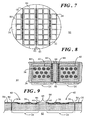
- FIG. 7 shows a top view of a controller wafer used in connection with the packaging process
- FIG. 8 shows an enlarged partial top view of the controller wafer
- FIG. 9 shows a partial side sectional view of the controller wafer of FIG. 7 ;
- FIG. 10 shows a partial side sectional view of the controller wafer at an initial stage of packaging in accordance with the packaging process
- FIG. 11 shows a partial side sectional view of the controller wafer of FIG. 10 at a subsequent stage of packaging
- FIG. 12 shows a partial bottom view of the controller wafer of FIG. 11 ;
- FIG. 13 shows a partial side sectional view of the controller wafer bonded to the sensor wafer to form a stacked wafer structure at a subsequent stage of packaging
- FIG. 14 shows a partial side sectional view of the stacked wafer structure of FIG. 13 at a subsequent stage of packaging
- FIG. 15 shows a partial side sectional view of the stacked wafer structure of FIG. 14 at a subsequent stage of packaging
- FIG. 16 shows a partial side sectional view of the stacked wafer structure of FIG. 15 at a subsequent stage of packaging
- FIG. 17 shows a partial side sectional view of the stacked wafer structure of FIG. 16 at a subsequent stage of packaging
- FIG. 18 shows a partial side sectional view of the stacked wafer structure of FIG. 17 at a subsequent stage of packaging
- FIG. 19 shows a partial side sectional view of the stacked wafer structure of FIG. 18 at a subsequent stage of packaging
- FIG. 20 shows a side sectional view of sensor packages produced from the stacked wafer structure of FIG. 19 in accordance with the packaging process of FIG. 3 .
- Semiconductor packages generally provide a set of related elements. These elements include, for example, one or more semiconductor devices to be packaged, interconnection from the devices to the package, a surrounding or containing structure to provide both mechanical support and electrical, chemical, and environmental protection, and a joining structure to attach the package to the board or system.
- the challenges faced by developers of semiconductor packaging processes result from, for example, the sensitivity of the semiconductor devices (e.g., microelectronics and microstructures) to high temperature processes, the need for suitable shielding, the requirement in some instances for a hermetic or near-hermetic seal to protect the devices from contaminants, and so forth.
- One or more of the semiconductor devices in a semiconductor package may be a microelectronic sensor (e.g., a magnetometer), a microelectromechanical systems (MEMS) sensor (e.g., an accelerometer, gyroscope, pressure sensor), or some other miniaturized sensor.
- MEMS microelectromechanical systems
- proper packaging is important to ensure the integrity of the signals to and from the sensor devices. For example, angular misalignment of a sensor device or multiple sensor devices in a sensor package can lead to inaccuracies in the measured signals. As such, precise angular alignment of sensors in a sensor package is critical for receiving accurate measurements.
- Angular alignment of sensors in traditional chip level packaging is currently limited to approximately plus or minus two degrees of accuracy.
- the angular alignment accuracy is limited by the tolerance of placement equipment utilized in die placement techniques. More precise angular alignment is being called for in the industry to improve the accuracy of measurements received from such sensors.
- IC integrated circuit
- Embodiments entail sensor packaging methodology and a sensor package produced in accordance with the packaging methodology.
- the packaging methodology involves a wafer-level packaging technique in lieu of traditional die-to-die placement techniques.
- Wafer-level packaging refers to packaging semiconductor devices at wafer level, and essentially extends the wafer fabrication process to include device interconnection and device protection processes.
- the wafer-level packaging process discussed herein provides high-throughput and precise placement packaging of sensors at relatively low cost. Additional advantages entail a chip-scale packaging technology that results in the sensor package being generally the same size as the die, stacking of sensors and microelectronic devices for size reduction, improved electrical performance, and so forth.
- FIG. 1 shows a top view of an exemplary sensor package 20 in accordance with an embodiment
- FIG. 2 shows a side view of sensor package 20 along section lines 2-2 in FIG. 1
- sensor package 20 includes a semiconductor die in the form of a sensor element 22 and another semiconductor die in the form of a controller element 24 bonded to sensor element 22.
- Sensor element 22 has a side 26 and another side 28 opposing side 26.
- side 26 is shown as being physically positioned above side 28.
- side 26 is referred to as an upper side 26 and the opposing side 28 is referred to as a lower side 28 for clarity of discussion.
- a sensor 30 and bond pads 32 are formed at upper side 26 of sensor element 22.
- Sensor 30 is positioned within an area 34 (best seen in FIG. 5 ) on upper side 26 delineated by a bonding perimeter 36 (best seen in FIG. 5 ).
- Bond pads 32 are positioned outside of area 34, external to bonding perimeter 36. Bond pads 32 may be electrically connected to various structures of sensor 30 by way of conductive vias, conductive material layers, and so forth in accordance with conventional and upcoming sensor device manufacturing processes.
- Sensor 30 may be a microelectromechanical systems (MEMS) sensor device such as an accelerometer, gyroscope, or some other sensor.
- MEMS microelectromechanical systems
- sensor 30 need not be limited to a MEMS sensor configuration.
- upper side 26 of sensor element 22 may include more than one sensor device positioned within area 34.
- Controller element 24 also has a side 38 and another side 40 opposing side 38.
- side 38 is shown as being physically positioned above side 40.
- side 38 is referred to as an upper side 38 and the opposing side 40 is referred to as a lower side 40 for clarity of discussion.
- Upper side 38 includes control circuitry 42 and bond pads 44 formed thereon.
- Lower side 40 includes a bonding perimeter 46 (best seen in FIG. 12 ) configured to abut bonding perimeter 36 of sensor element 22. Bonding perimeter 46 of controller element 24 is coupled to bonding perimeter 36 to form a stacked wafer structure 48 in which at least lower side 40 of controller element 24 is co-aligned with upper side 26 of sensor element 22.
- Control circuitry 42 may be any active or passive circuitry used in the "active area" of controller element 24 and used to communicate signals to and from sensor 30.
- Bond wires 50 are attached between corresponding bond pads 32 on upper side 26 of sensor element 22 and bond pads 44 on upper side 38 of controller element 24 to provide suitable electrical interconnections between controller element 24 and sensor element 22.
- features may be formed on lower side 40 of controller element 24.
- these features can include functional components of sensor 30 located on upper side 26 such as, one or more cavities 52 and one or more electrodes 54.
- Cavities 52 and electrodes 54 may be formed within the boundary of bonding perimeter 46 and are generally aligned with sensors 30.
- a sensor 55 may be formed integrally with the passive and active elements of control circuitry 42 within controller element 24 in accordance with conventional and upcoming semiconductor manufacturing processes.
- the various elements of control circuitry 42 and the integral sensor 55 are represented by the variety of shading and elements internal to controller element 24.
- sensor package 20 may include a sensor die 56 mounted on upper side 38 of controller element 24.
- integral sensor 55 or sensor die 56 may be a magnetometer for measuring the strength or direction of magnetic fields.
- integral sensor 55 or sensor die 56 may be some other sensor device in accordance with particular design criteria for sensor package 20.
- Controller element 24 further includes bump pads 58 formed on and distributed across upper side 38.
- conductive elements 60 are formed on bump pads 58 after controller element 24 is bonded to sensor element 22.
- Conductive elements 60 may be pillars, balls, plugs, or some other conductive features that extend above bump pads 58. Conductive elements 60 are utilized as input/output elements for sensor package 20.
- a packaging material 62 is applied over upper side 38 of controller element 24 to encapsulate control circuitry 42, sensor element 22, and bond wires 50, and to at least partially encapsulate conductive elements 60 so that only a top side 64 of conductive elements 60 is exposed from packaging material 62.
- Packaging material 62 may be any conventional molding compound such as, for example, an epoxy resin material.
- Sensor package 20 is provided herein for exemplary purposes. However, sensor package 20 may take on a wide variety of forms, sizes, shapes, and functions in accordance with particular design criteria.
- FIG. 3 shows a flowchart of a packaging process 70 for fabricating sensor package 20 of FIG. 1 in accordance with another embodiment.
- Packaging process 70 sets forth a wafer-level packaging technique in which semiconductor dies are packaged while still in the wafer followed by wafer dicing, in lieu of traditional die placement techniques.
- Packaging process 70 will be discussed in connection with the packaging of a plurality of sensor packages 20 ( FIG. 1 ). However, it should become apparent that the following methodology can be adapted to packaging methodology for a multiplicity of semiconductor designs.
- Packaging process 70 sets forth an exemplary flow of operations for clarity of discussion. However, in actual practice there may be variations in the order of operations in accordance with particular processing capabilities of a packaging facility.
- Packaging process 70 begins with an activity 72.
- a sensor wafer is provided with a multiplicity of sensors 30 ( FIG. 2 ) formed thereon.
- the sensor wafer may be provided from a device manufacturer and packaged in accordance with packaging process 70 at a separate packaging facility. Alternatively, the sensor wafer may be fabricated and packaged within the same manufacturing facility.
- FIG. 4 shows a top view of a sensor wafer 74 used in connection with packaging process 70.
- FIG. 5 shows a partial top view of sensor wafer 74 with sensors 30 formed on upper side 26 thereof, and
- FIG. 6 shows a partial side sectional view of sensor wafer 74.
- the following FIGs. 4-20 may be illustrated using various shading and/or hatching to distinguish the different elements, as will be discussed below. These different elements may be produced utilizing current and upcoming micromachining techniques.
- FIG. 4 particularly illustrates an exemplary sensor wafer 74 having a plurality of sensor elements 22 formed on a silicon-based substrate.
- Sensor elements 22 may be any of a plurality of sensor devices such as inertial sensors, gyroscopes, optical devices, pressure sensors, magnetic field sensors, switches, microphones, and so forth.
- sensor elements 22 may be any other device in which it is desirable to individually protect, i.e., cap, sensitive features and additionally expose or reveal terminal elements, i.e., bond pads 32 ( FIG. 2 ) at the wafer level.
- Sensor wafer 74 may be manufactured utilizing conventional and upcoming bulk micromachining, surface micromachining, and/or high aspect ratio silicon micromachining techniques. Fabrication processes for a surface micromachining technique can generally include, for example, deposition, patterning, and etching of one or more sacrificial oxide layers, one or more structural polysilicon layers, and the like. For example, one or more sacrificial oxide layers may be deposited overlying the silicon-based wafer, and one or more structural layers may then be deposited over the sacrificial layers. A structural layer can then be suitably patterned and etched to form the movable and non-movable microstructures 76 of sensors 30, as well as bond pads 32 of sensor elements 22. Additionally, deposition of a bonding material, such as a metallization layer, at bonding perimeter 36 may be performed. The bonding material will form part of a seal ring between sensor wafer 74 and a controller wafer (discussed below).
- a bonding material such as a metallization layer
- sensor wafer 74 may be identical, or sensor wafer 74 can contain a mixture of sensor elements.
- Dashed lines 78 represent borders delineating the various sensor elements 22 formed on sensor wafer 74.
- Dashed lines 78 can additionally represent the locations at which sensor wafer 74 will eventually be singulated (discussed below). Thus, dashed lines 78 are referred to hereinafter as saw lines 78.
- Sensor wafer 74 is illustrated as being generally disk-shaped. However, alternative embodiments of sensor wafer 74 may be any suitable shape, such as rectangular shaped. The quantity of sensor elements 22 formed on a given sensor wafer 74 varies depending upon the size of sensor elements 22 and upon the size of sensor wafer 74.
- packaging process 70 continues with an activity 80.
- a controller wafer is provided with a multiplicity of controller elements 24 ( FIG. 2 ) formed thereon.
- the controller wafer may be provided from a device manufacturer and packaged in accordance with packaging process 70 at a separate packaging facility. Alternatively, the controller wafer may be fabricated and packaged within the same manufacturing facility.
- FIG. 7 shows a top view of a controller wafer 82 used in connection with packaging process 70.
- FIG. 8 shows an enlarged partial top view of controller wafer 82 with connections to control circuitry 42 (generally represented by rectangles) of controller elements 24 on upper side 38
- FIG. 9 shows a partial side sectional view of controller wafer 82.
- Controller wafer 82 may be manufactured utilizing conventional and upcoming integrated circuit (IC) fabrication techniques for forming control circuitry 42 in the active regions of controller wafer 82.
- IC integrated circuit
- the implementation of standard IC wafer fabrication techniques creates transistors, capacitors, resistors, diodes, and all other components of control circuitry 42.
- these IC fabrication techniques may be implemented to form bond pads 44 and bumps pads 58 at upper side 38 of controller wafer 82. These conventional process steps need not be described herein.
- dashed lines 84 represent the locations at which controller wafer 82 will be sawn or diced in at least two separate operations. For example, in the illustrated embodiment, immediately adjacent pairs 85 of vertically arranged dashed lines 84 represent the locations at which portions (discussed below) of controller wafer 82 will be removed in order to access bond pads 32 ( FIG. 4 ) of the underlying sensor wafer 74 ( FIG. 4 ). The remaining dashed lines 84 represent the locations at which controller wafer 82 will eventually be singulated (discussed below) concurrent with singulation of sensor wafer 74. Dashed lines 84 are collectively referred to herein as saw lines 84.
- Controller wafer 82 is illustrated as being generally disk-shaped to correspond with sensor wafer 74 ( FIG. 4 ). However, alternative embodiments of controller wafer 82 may be any suitable shape, such as rectangular shaped. Additionally, the quantity of controller elements 24 formed on a given controller wafer 82 varies depending upon the size of controller elements 24 and upon the size of controller wafer 82.
- controller wafer 82 undergoes a backgrinding process to thin wafer 82.
- lower side 40 undergoes backgrinding, also referred to as wafer thinning, using a conventional abrasive material and equipment.
- FIG. 10 shows a partial side sectional view of controller wafer 82 at an initial stage 88 of packaging in accordance with packaging process 70.
- controller wafer 82 exhibits an initial thickness 90 when it is provided for packaging at activity 80.
- Initial thickness 90 of controller wafer 88 may be roughly seven hundred fifty microns thick.
- Wafer backgrinding is a semiconductor device fabrication operation in which wafer thickness is reduced to enable stacking and high density packaging of semiconductor devices.
- a final thickness 92 of controller wafer 82 following execution of backgrinding activity 86 is less than initial thickness 90.
- Final thickness 92 can be any suitable dimension that is as thin as possible without unduly sacrificing mechanical stability, while still enabling features, e.g., cavities 52 ( FIG. 2 ) and/or electrodes 54 ( FIG. 2 ) to be formed at lower side 40 of controller wafer 82.
- final thickness 92 of controller wafer 82 may be roughly five hundred microns.
- packaging process 70 continues with an activity 94.
- features such as cavities 52 and/or electrodes 54 ( FIG. 2 ) may be formed at lower side 40 of controller wafer 82 in accordance with particular design criteria for sensor package 20 ( FIG. 2 ).
- Packaging process 70 continues with an activity 96 at which a bonding material is applied to lower side of controller wafer 82.
- FIG. 11 shows a partial side sectional view of controller wafer 82 of FIG. 10 at a subsequent stage 95 of packaging
- FIG. 12 shows a partial bottom view of controller wafer 82 at subsequent stage 96.
- cavities 52 may be created from lower side 40 extending partially through controller wafer 82.
- Cavities 52 may be formed by etching through controller wafer 82 from lower side 40.
- cavities 52 may be created by performing a deep-reactive ion etch (DRIE) process, another anisotropic etch process, a silicon etch process, and so forth to form cavities 52 in controller wafer 82.
- DRIE deep-reactive ion etch
- electrodes 54 may be formed on lower side 40 by, for example, the conventional semiconductor processes of deposition, patterning, and etching of insulating and conductive material. As known to those skilled in the art, electrodes 54 should be electrically isolated form the bulk semiconductor silicon of controller element 24 by an insulating layer. This insulating layer is not distinctly shown for simplicity of illustration.
- bonding layer 98 may be metallization.
- the term metallization refers to a metal layer that serves primarily as a means of electrical contact and interconnection within semiconductor devices.
- a metal layer is typically utilized in order to avoid contamination of other systems, such as a chemical vapor deposition (CVD) system, an epi deposition system, and the like.
- CVD chemical vapor deposition
- Thin-film aluminum is the most widely used metallization in semiconductor manufacturing, and may be deposited by sputtering, dual source evaporation or electroplating.
- electrodes 54 may be formed concurrent with the application of bonding layer 98 to bonding perimeter 46. However, electrodes 54 may alternatively be formed in a different process.
- bonding material 98 e.g., metallization
- bonding material 98 may alternatively or additionally be applied to bonding perimeter 36 of sensor wafer 74, as mentioned above.
- controller wafer 82 is bonded to sensor wafer 74 to form stacked wafer structure 48 ( FIG. 2 ).
- FIG. 13 shows a partial side sectional view of controller wafer 82 bonded to sensor wafer 74 to form stacked wafer structure 48 at a subsequent stage 104 of packaging. More particularly, bonding perimeters 46 located on lower side 40 of controller wafer 82 are bonded to corresponding bonding perimeters 36 of sensor wafer 74. Thus, following bonding activity 100, controller wafer 82 becomes a cap for protecting the movable and non-movable microstructures 76 located at upper side 26 of sensor wafer 74.
- Bonding may be performed utilizing, for example, eutectic bonding.
- Eutectic bonding also referred to as eutectic soldering, refers to a wafer bonding technique with an intermediate eutectic metal layer, e.g., metallization 98 ( FIG. 12 ).
- a eutectic metal layer is an alloy that transforms directly from solid to liquid state, or vice versa, at a specific composition and temperature without passing a two-phase equilibrium, i.e., liquid and solid state. Therefore, the eutectic temperature of the eutectic metal layer can be much lower than the melting temperature of the two or more pure elements that make up the eutectic metal layer.
- Eutectic bonding is able to produce hermetically sealed packages and electrical interconnection at relatively low processing temperatures using a single process. Additional attributes of eutectic bonding include low resultant stress induced in final assembly, high bonding strength, large fabrication yield, and a good reliability. Although, eutectic bonding is discussed therein, it should be understood that any other suitable bonding technique may alternatively be implemented.
- Alignment of controller wafer 82 with sensor wafer 74 may be achieved by utilizing mechanical or optical fiducial marks, such as notches at the edges of wafers 74 and 82, pins, etchings, or holographic images, among others.
- Automatic process equipment for silicon wafer bonding, as well as the integration of suitable alignment techniques can provide precision location keyed to specific features on the semiconductor elements of wafers 74 and 82.
- angular alignment of less than one tenth of a degree of accuracy for the sensors may be achieved. This alignment accuracy is in contrast with the angular alignment of sensors achieved in traditional chip level die packaging, which is typically limited to approximately plus or minus two degrees of accuracy.
- packaging process 70 continues with an activity 106 following bonding activity 100.
- sensor wafer 74 of stacked wafer structure 48 undergoes a backgrinding, or wafer thinning process using a conventional abrasive material and equipment.
- FIG. 14 shows a partial side sectional view of stacked wafer structure 48 at a subsequent stage 108 of packaging.
- sensor wafer 74 exhibits an initial thickness 110 when it is provided for packaging at activity 72 ( FIG. 3 ).
- Initial thickness 110 of sensor wafer 74 may be roughly 700 microns or greater.
- Wafer backgrinding can be performed to reduce the thickness of sensor wafer 74.
- a final thickness 112 of sensor wafer 74 following execution of backgrinding activity 106 is less than initial thickness 110.
- final thickness 112 of sensor wafer 74 following backgrinding may be roughly three hundred microns.
- packaging process 70 continues with an activity 114.
- conductive elements 60 ( FIG. 2 ) are formed on bump pads 58 ( FIG. 9 ) of controller wafer 82 ( FIG. 9 ).
- FIG. 15 shows a partial side sectional view of stacked wafer structure 48 at a subsequent stage 116 of packaging.
- conductive elements 60 are formed on bump pads 58 of controller wafer 82.
- Conductive elements 60 may be copper pillars that are plated onto bump pads 58 of controller wafer 82. Alternatively, stud bumps or solder balls may be attached to bump pads 58 in accordance with conventional processes.
- Conductive elements 60 are formed on bump pads 58 of the bonded wafers of stacked structure 48 as a wafer-level process to achieve improvements in rotational accuracy of sensor package 20 to the product circuit.
- Formation of conductive elements 60 as a wafer-level process achieves accuracy improvements as compared with assembling a die into a sensor package, followed by assembling the sensor package into a product circuit. Accordingly, when sensor package 20 ( FIG. 2 ) is eventually assembled to a product circuit by, for example, soldering, the location and rotation of sensor package 20 relative to the product circuit will be determined by the location and rotation of conductive elements 60 because the solder will align conductive elements 60 to the corresponding features on the product circuit.
- packaging process 70 continues with an activity 118.
- sensor dies 56 when sensor dies 56 ( FIG. 2 ) are part of the design configuration, sensor dies 56 may be mounted to controller wafer 82 at suitable locations directly on controller elements 24 of controller wafer 82.
- FIG. 16 shows a partial side sectional view of stacked wafer structure 48 at a subsequent stage 120 of packaging.
- Sensor dies 56 may be bonded to controller wafer 82 by a die attach process and wire bonded to controller wafer 82.
- sensor dies 56 may be mounted to controller wafer 82 utilizing a flip chip technique in which sensor dies 56 are inverted and connected directly to controller elements 24 using, for example, solder bump mounting, stud bump bonding, and the like, rather than a conventional wire bonding technique.
- a flip chip technique may achieve good rotation and tilt accuracy between sensor dies 56 and sensors 30 of the underlying sensor wafer 74.
- even implementation of a die attach process may achieve improvements in alignment accuracy between sensor dies 56 and sensors 30 since each controller element 24 on controller wafer 82 is bonded to the underlying sensor element 22 containing sensor 30 with the excellent rotation and tilt accuracies achieved with wafer-to-wafer bonding. More critically, however, the mounting of sensor dies 56 onto controller wafer 82 can achieve improved package density.
- packaging process 70 continues with an activity 122 following activity 118.
- portions of controller wafer 82 are removed to reveal bond pads 32 ( FIG. 2 ) on sensor wafer 74.
- FIG. 17 shows a partial side sectional view of stacked wafer structure 48 at a subsequent stage 124 of packaging.
- portions 126 of controller wafer 82 are removed to expose, i.e., reveal, bond pads 32, of the underlying sensor wafer 74.
- Portions 126 may be removed by sawing along adjacent pairs 85 (see FIG. 16 ) of saw lines 84 in controller wafer 82.
- controller wafer 82 Once portions 126 of controller wafer 82 have been removed to expose, i.e., reveal, bond pads 32 at activity 122, packaging process 70 continues with an activity 128. At activity 128, bond wires 50 ( FIG. 2 ) are attached between bond pads 32 ( FIG. 2 ) of sensor wafer 74 and bond pads 44 ( FIG. 2 ) of controller wafer 82.
- FIG. 18 shows a partial side sectional view of stacked wafer structure 48 at a subsequent stage 130 of packaging.
- bond wires 50 are bonded to bond pads 32 on upper side 26 of sensor wafer 74 and to corresponding bond pads 44 on upper side 38 of controller wafer 82 using a conventional wire bonding process.
- conductive elements 60 are higher than the wire bond loop height of bond wires 50.
- Wire bonding is a cost-effective and flexible interconnect technique, and can be readily implemented when forming electrical interconnects during a wafer-level fabrication process.
- packaging process 70 continues with an activity 132.
- packaging material 62 FIG. 2
- packaging material 62 FIG. 2
- FIG. 19 shows a partial side sectional view of stacked wafer structure 48 at a subsequent stage 134 of packaging.
- packaging material 62 may be mold compound, potting compound, epoxy resin, and so forth, and packaging material 62 is applied in a thick enough layer to cover bond wires 50 and conductive elements 60. If packaging material 62 entirely covers conductive elements 60 during encapsulation, packaging material 62 may be ground down or otherwise abraded to expose top surface 64 of conductive elements 60 without exposing bond wires 50.
- continued processing may be performed which is not shown herein for brevity.
- This continued processing may entail the addition of solder balls above conductive elements 60.
- the added solder balls can increase standoff and improve the electrical interconnection
- Additional continued processing may entail visual inspection, operational testing, burn-in, stress testing, accelerated life testing, the build-up of additional redistribution layers above packaging material 62 and top surface 64 of conductive elements, and so forth all while still at wafer level.
- an activity 136 is eventually performed.
- the fabricated stacked wafer structure 48 is singulated, i.e., cut, punched, or diced, in a conventional manner.
- packaging process 70 ends.
- FIG. 20 shows a side sectional view of sensor packages 20 produced from stacked wafer structure 48 ( FIG. 19 ) in accordance with packaging process 70.
- stacked wafer structure 48 has been singulated, i.e., cut, punched, or diced, along saw lines that correspond with saw lines 78 (see FIG. 19 ) of sensor wafer 74 and the remaining saw lines 84 (see FIG. 19 ) of controller wafer 82 to provide individual sensor packages 20.
- the individual sensor packages 20 can be coupled onto, for example, a printed circuit board in an end application.
- Each of the resulting sensor packages 20 represents a chip-scale package in which the x and y package dimensions are approximately equivalent to the x and y dimensions of sensor element 22.
- the z dimension, i.e., the thickness, of each sensor package 20 is approximately one hundred to two hundred microns larger than the thickness of the stacked wafer structure in order to accommodate conductive elements 60 and bond wires 50.
- Embodiments described herein entail microelectronic sensor packaging methodology and a sensor package produced in accordance with the packaging methodology.
- the packaging methodology involves a wafer-level packaging technique in lieu of traditional die placement techniques.
- the controller wafer is bonded to a sensor wafer to form a stacked wafer structure with the active side of the controller wafer facing outwardly from the package.
- the package inputs and outputs can be formed on the controller wafer.
- a portion of the stacked wafer structure is sawn, etched, or otherwise cut to reveal the underlying bond pads of the sensor wafer and the corresponding bond pads for the controller elements on the controller wafer are wire bonded to the sensor bond pads in wafer format.
- the wafer-level packaging process is especially suitable for the packaging of miniaturized sensors where precise rotation and tilt accuracy of the sensors can be achieved at the wafer level, rather than at the die level. Moreover, the required angular accuracy can be assured without more costly and time consuming testing. Accordingly, the wafer-level packaging process discussed herein provides high-throughput and precise placement packaging of sensors at relatively low cost. Moreover, the wafer-level packaging process results in individual sensor packages that are generally the same size as the die, stacking of sensors and microelectronic devices for size reduction and improved package density, enhanced electrical performance, and so forth. Additionally, the wafer structure and corresponding methodology are cost-effective, readily implemented, and adaptable to existing assembly and packaging tools and techniques.
Landscapes
- Engineering & Computer Science (AREA)
- Microelectronics & Electronic Packaging (AREA)
- Manufacturing & Machinery (AREA)
- Computer Hardware Design (AREA)
- Micromachines (AREA)
- Wire Bonding (AREA)
- Pressure Sensors (AREA)
Applications Claiming Priority (1)
| Application Number | Priority Date | Filing Date | Title |
|---|---|---|---|
| US13/546,902 US9040355B2 (en) | 2012-07-11 | 2012-07-11 | Sensor package and method of forming same |
Related Parent Applications (1)
| Application Number | Title | Priority Date | Filing Date |
|---|---|---|---|
| US13/546,902 Previously-Filed-Application US9040355B2 (en) | 2012-07-11 | 2012-07-11 | Sensor package and method of forming same |
Publications (3)
| Publication Number | Publication Date |
|---|---|
| EP2684837A2 true EP2684837A2 (de) | 2014-01-15 |
| EP2684837A3 EP2684837A3 (de) | 2014-08-13 |
| EP2684837B1 EP2684837B1 (de) | 2019-05-15 |
Family
ID=48747334
Family Applications (1)
| Application Number | Title | Priority Date | Filing Date |
|---|---|---|---|
| EP13173238.0A Active EP2684837B1 (de) | 2012-07-11 | 2013-06-21 | Sensorgehäuse auf Waferebene und Verfahren zu dessen Herstellung |
Country Status (3)
| Country | Link |
|---|---|
| US (2) | US9040355B2 (de) |
| EP (1) | EP2684837B1 (de) |
| CN (1) | CN103569956B (de) |
Cited By (1)
| Publication number | Priority date | Publication date | Assignee | Title |
|---|---|---|---|---|
| EP2942807A1 (de) * | 2014-05-07 | 2015-11-11 | Sensirion AG | Halbleiterpaket |
Families Citing this family (15)
| Publication number | Priority date | Publication date | Assignee | Title |
|---|---|---|---|---|
| FR3008690B1 (fr) * | 2013-07-22 | 2016-12-23 | Commissariat Energie Atomique | Dispositif comportant un canal fluidique muni d'au moins un systeme micro ou nanoelectronique et procede de realisation d'un tel dispositif |
| WO2015020881A1 (en) * | 2013-08-05 | 2015-02-12 | Robert Bosch Gmbh | Inertial and pressure sensors on single chip |
| US9242851B2 (en) | 2013-08-06 | 2016-01-26 | Freescale Semiconductor, Inc | MEMS device with differential vertical sense electrodes |
| US9738511B2 (en) * | 2013-09-13 | 2017-08-22 | Invensense, Inc. | Reduction of chipping damage to MEMS structure |
| US9553208B2 (en) * | 2013-09-16 | 2017-01-24 | Infineon Technologies Ag | Current sensor device |
| US9627346B2 (en) * | 2013-12-11 | 2017-04-18 | Taiwan Semiconductor Manufacturing Company, Ltd. | Underfill pattern with gap |
| KR20150141417A (ko) * | 2014-06-10 | 2015-12-18 | 삼성전기주식회사 | 다축센서 |
| KR20170104496A (ko) | 2015-01-28 | 2017-09-15 | 콘티넨탈 테베스 아게 운트 코. 오하게 | 대칭적으로 매립된 센서 엘리먼트들을 갖는 센서 |
| CN107209034B (zh) | 2015-01-28 | 2020-03-24 | 大陆-特韦斯股份有限公司 | 具有用于传感器的嵌入式过滤器部件的适配器 |
| US9969614B2 (en) | 2015-05-29 | 2018-05-15 | Taiwan Semiconductor Manufacturing Company, Ltd. | MEMS packages and methods of manufacture thereof |
| US9550667B1 (en) | 2015-09-08 | 2017-01-24 | Taiwan Semiconductor Manufactruing Company Ltd. | Semiconductor structure and manufacturing method thereof |
| US10364140B2 (en) * | 2015-09-22 | 2019-07-30 | Nxp Usa, Inc. | Integrating diverse sensors in a single semiconductor device |
| CN106477510B (zh) * | 2016-11-29 | 2018-03-20 | 合肥芯福传感器技术有限公司 | 堆叠式mems传感器封装体、芯片及其制作方法 |
| IT202200022395A1 (it) | 2022-10-31 | 2024-05-01 | St Microelectronics Srl | Procedimento di fabbricazione di un dispositivo comprendente due piastrine semiconduttrici e dispositivo cosi' ottenuto |
| US20240418510A1 (en) * | 2023-06-15 | 2024-12-19 | AAC Technologies Pte. Ltd. | Inertial sensor and method for forming the same |
Family Cites Families (27)
| Publication number | Priority date | Publication date | Assignee | Title |
|---|---|---|---|---|
| US6853067B1 (en) | 1999-10-12 | 2005-02-08 | Microassembly Technologies, Inc. | Microelectromechanical systems using thermocompression bonding |
| US6522015B1 (en) | 2000-09-26 | 2003-02-18 | Amkor Technology, Inc. | Micromachine stacked wirebonded package |
| AUPR245301A0 (en) | 2001-01-10 | 2001-02-01 | Silverbrook Research Pty Ltd | An apparatus (WSM06) |
| US6891239B2 (en) * | 2002-03-06 | 2005-05-10 | The Charles Stark Draper Laboratory, Inc. | Integrated sensor and electronics package |
| US6838776B2 (en) | 2003-04-18 | 2005-01-04 | Freescale Semiconductor, Inc. | Circuit device with at least partial packaging and method for forming |
| US6921975B2 (en) | 2003-04-18 | 2005-07-26 | Freescale Semiconductor, Inc. | Circuit device with at least partial packaging, exposed active surface and a voltage reference plane |
| US7368808B2 (en) * | 2003-06-30 | 2008-05-06 | Intel Corporation | MEMS packaging using a non-silicon substrate for encapsulation and interconnection |
| US7256074B2 (en) | 2003-10-15 | 2007-08-14 | Micron Technology, Inc. | Methods for wafer-level packaging of microelectronic devices and microelectronic devices formed by such methods |
| US7104129B2 (en) | 2004-02-02 | 2006-09-12 | Invensense Inc. | Vertically integrated MEMS structure with electronics in a hermetically sealed cavity |
| US7202560B2 (en) * | 2004-12-15 | 2007-04-10 | Avago Technologies Wireless Ip (Singapore) Pte. Ltd. | Wafer bonding of micro-electro mechanical systems to active circuitry |
| US7442570B2 (en) | 2005-03-18 | 2008-10-28 | Invensence Inc. | Method of fabrication of a AL/GE bonding in a wafer packaging environment and a product produced therefrom |
| US7295029B2 (en) | 2005-03-24 | 2007-11-13 | Memsic, Inc. | Chip-scale package for integrated circuits |
| US7352039B2 (en) * | 2005-03-24 | 2008-04-01 | Intel Corporation | Methods and apparatuses for microelectronic assembly having a material with a variable viscosity around a MEMS device |
| US7364945B2 (en) | 2005-03-31 | 2008-04-29 | Stats Chippac Ltd. | Method of mounting an integrated circuit package in an encapsulant cavity |
| US7419853B2 (en) | 2005-08-11 | 2008-09-02 | Hymite A/S | Method of fabrication for chip scale package for a micro component |
| FI119728B (fi) | 2005-11-23 | 2009-02-27 | Vti Technologies Oy | Menetelmä mikroelektromekaanisen komponentin valmistamiseksi ja mikroelektromekaaninen komponentti |
| US7384819B2 (en) * | 2006-04-28 | 2008-06-10 | Freescale Semiconductor, Inc. | Method of forming stackable package |
| US7446017B2 (en) | 2006-05-31 | 2008-11-04 | Freescale Semiconductor, Inc. | Methods and apparatus for RF shielding in vertically-integrated semiconductor devices |
| US20080246126A1 (en) | 2007-04-04 | 2008-10-09 | Freescale Semiconductor, Inc. | Stacked and shielded die packages with interconnects |
| EP2011762B1 (de) * | 2007-07-02 | 2015-09-30 | Denso Corporation | Halbleiterbauelement mit einem Sensor, der mit einem externen Element verbunden ist |
| JP4404143B2 (ja) * | 2007-07-02 | 2010-01-27 | 株式会社デンソー | 半導体装置およびその製造方法 |
| US7858440B2 (en) | 2007-09-21 | 2010-12-28 | Infineon Technologies Ag | Stacked semiconductor chips |
| US8089144B2 (en) | 2008-12-17 | 2012-01-03 | Denso Corporation | Semiconductor device and method for manufacturing the same |
| US7868729B2 (en) | 2009-03-03 | 2011-01-11 | Freescale Semiconductor, Inc. | Stacked device assembly with integrated coil and method of forming same |
| CN101533832A (zh) * | 2009-04-14 | 2009-09-16 | 李刚 | 微机电系统器件与集成电路的集成芯片及集成方法 |
| US8551814B2 (en) | 2010-03-11 | 2013-10-08 | Freescale Semiconductor, Inc. | Method of fabricating a semiconductor device that limits damage to elements of the semiconductor device that are exposed during processing |
| CN102241388B (zh) * | 2011-05-18 | 2015-02-18 | 中国科学院上海微系统与信息技术研究所 | Mems圆片级三维混合集成封装结构及方法 |
-
2012
- 2012-07-11 US US13/546,902 patent/US9040355B2/en active Active
-
2013
- 2013-06-21 EP EP13173238.0A patent/EP2684837B1/de active Active
- 2013-07-10 CN CN201310287464.0A patent/CN103569956B/zh active Active
-
2014
- 2014-10-29 US US14/527,567 patent/US20150048462A1/en not_active Abandoned
Non-Patent Citations (1)
| Title |
|---|
| None |
Cited By (2)
| Publication number | Priority date | Publication date | Assignee | Title |
|---|---|---|---|---|
| EP2942807A1 (de) * | 2014-05-07 | 2015-11-11 | Sensirion AG | Halbleiterpaket |
| US9437514B2 (en) | 2014-05-07 | 2016-09-06 | Sensirion Ag | Semiconductor package with coated side walls and method of manufacture |
Also Published As
| Publication number | Publication date |
|---|---|
| US20150048462A1 (en) | 2015-02-19 |
| US20140015123A1 (en) | 2014-01-16 |
| EP2684837A3 (de) | 2014-08-13 |
| US9040355B2 (en) | 2015-05-26 |
| CN103569956A (zh) | 2014-02-12 |
| EP2684837B1 (de) | 2019-05-15 |
| CN103569956B (zh) | 2017-04-12 |
Similar Documents
| Publication | Publication Date | Title |
|---|---|---|
| US9040355B2 (en) | Sensor package and method of forming same | |
| US9165886B2 (en) | Sensor packaging method and sensor packages | |
| US8709868B2 (en) | Sensor packages and method of packaging dies of differing sizes | |
| US9376310B2 (en) | Microelectronic packages having stacked accelerometer and magnetometer die and methods for the production thereof | |
| US9574959B2 (en) | Various stress free sensor packages using wafer level supporting die and air gap technique | |
| US7419853B2 (en) | Method of fabrication for chip scale package for a micro component | |
| US8836132B2 (en) | Vertical mount package and wafer level packaging therefor | |
| US20040259325A1 (en) | Wafer level chip scale hermetic package | |
| US10435290B2 (en) | Wafer level package for a MEMS sensor device and corresponding manufacturing process | |
| US7614301B2 (en) | Acceleration sensor chip package and method of producing the same | |
| US20130320463A1 (en) | Package structure having mems element and fabrication method thereof | |
| US20140048946A1 (en) | Sensor packages and method of packaging dies of various sizes | |
| US7833815B2 (en) | Microelectromechanical system package and the method for manufacturing the same | |
| EP2520541B1 (de) | Systeme und Verfahren für dreiachsige Sensorchipgehäuse | |
| US7932570B1 (en) | Silicon tab edge mount for a wafer level package | |
| EP4361091A1 (de) | Verfahren zur herstellung einer vorrichtung mit zwei halbleiterchips und so erhaltene vorrichtung | |
| CN221440346U (zh) | 半导体器件和微机电系统 |
Legal Events
| Date | Code | Title | Description |
|---|---|---|---|
| PUAI | Public reference made under article 153(3) epc to a published international application that has entered the european phase |
Free format text: ORIGINAL CODE: 0009012 |
|
| AK | Designated contracting states |
Kind code of ref document: A2 Designated state(s): AL AT BE BG CH CY CZ DE DK EE ES FI FR GB GR HR HU IE IS IT LI LT LU LV MC MK MT NL NO PL PT RO RS SE SI SK SM TR |
|
| AX | Request for extension of the european patent |
Extension state: BA ME |
|
| PUAL | Search report despatched |
Free format text: ORIGINAL CODE: 0009013 |
|
| AK | Designated contracting states |
Kind code of ref document: A3 Designated state(s): AL AT BE BG CH CY CZ DE DK EE ES FI FR GB GR HR HU IE IS IT LI LT LU LV MC MK MT NL NO PL PT RO RS SE SI SK SM TR |
|
| AX | Request for extension of the european patent |
Extension state: BA ME |
|
| RIC1 | Information provided on ipc code assigned before grant |
Ipc: B81C 1/00 20060101AFI20140709BHEP |
|
| 17P | Request for examination filed |
Effective date: 20150213 |
|
| RBV | Designated contracting states (corrected) |
Designated state(s): AL AT BE BG CH CY CZ DE DK EE ES FI FR GB GR HR HU IE IS IT LI LT LU LV MC MK MT NL NO PL PT RO RS SE SI SK SM TR |
|
| 17Q | First examination report despatched |
Effective date: 20161018 |
|
| RAP1 | Party data changed (applicant data changed or rights of an application transferred) |
Owner name: NXP USA, INC. |
|
| STAA | Information on the status of an ep patent application or granted ep patent |
Free format text: STATUS: EXAMINATION IS IN PROGRESS |
|
| GRAP | Despatch of communication of intention to grant a patent |
Free format text: ORIGINAL CODE: EPIDOSNIGR1 |
|
| STAA | Information on the status of an ep patent application or granted ep patent |
Free format text: STATUS: GRANT OF PATENT IS INTENDED |
|
| INTG | Intention to grant announced |
Effective date: 20181119 |
|
| GRAJ | Information related to disapproval of communication of intention to grant by the applicant or resumption of examination proceedings by the epo deleted |
Free format text: ORIGINAL CODE: EPIDOSDIGR1 |
|
| STAA | Information on the status of an ep patent application or granted ep patent |
Free format text: STATUS: EXAMINATION IS IN PROGRESS |
|
| INTC | Intention to grant announced (deleted) | ||
| GRAP | Despatch of communication of intention to grant a patent |
Free format text: ORIGINAL CODE: EPIDOSNIGR1 |
|
| STAA | Information on the status of an ep patent application or granted ep patent |
Free format text: STATUS: GRANT OF PATENT IS INTENDED |
|
| GRAS | Grant fee paid |
Free format text: ORIGINAL CODE: EPIDOSNIGR3 |
|
| GRAA | (expected) grant |
Free format text: ORIGINAL CODE: 0009210 |
|
| STAA | Information on the status of an ep patent application or granted ep patent |
Free format text: STATUS: THE PATENT HAS BEEN GRANTED |
|
| INTG | Intention to grant announced |
Effective date: 20190403 |
|
| AK | Designated contracting states |
Kind code of ref document: B1 Designated state(s): AL AT BE BG CH CY CZ DE DK EE ES FI FR GB GR HR HU IE IS IT LI LT LU LV MC MK MT NL NO PL PT RO RS SE SI SK SM TR |
|
| REG | Reference to a national code |
Ref country code: CH Ref legal event code: EP Ref country code: GB Ref legal event code: FG4D |
|
| REG | Reference to a national code |
Ref country code: DE Ref legal event code: R096 Ref document number: 602013055332 Country of ref document: DE |
|
| REG | Reference to a national code |
Ref country code: IE Ref legal event code: FG4D |
|
| REG | Reference to a national code |
Ref country code: NL Ref legal event code: MP Effective date: 20190515 |
|
| REG | Reference to a national code |
Ref country code: LT Ref legal event code: MG4D |
|
| PG25 | Lapsed in a contracting state [announced via postgrant information from national office to epo] |
Ref country code: FI Free format text: LAPSE BECAUSE OF FAILURE TO SUBMIT A TRANSLATION OF THE DESCRIPTION OR TO PAY THE FEE WITHIN THE PRESCRIBED TIME-LIMIT Effective date: 20190515 Ref country code: AL Free format text: LAPSE BECAUSE OF FAILURE TO SUBMIT A TRANSLATION OF THE DESCRIPTION OR TO PAY THE FEE WITHIN THE PRESCRIBED TIME-LIMIT Effective date: 20190515 Ref country code: NO Free format text: LAPSE BECAUSE OF FAILURE TO SUBMIT A TRANSLATION OF THE DESCRIPTION OR TO PAY THE FEE WITHIN THE PRESCRIBED TIME-LIMIT Effective date: 20190815 Ref country code: PT Free format text: LAPSE BECAUSE OF FAILURE TO SUBMIT A TRANSLATION OF THE DESCRIPTION OR TO PAY THE FEE WITHIN THE PRESCRIBED TIME-LIMIT Effective date: 20190915 Ref country code: HR Free format text: LAPSE BECAUSE OF FAILURE TO SUBMIT A TRANSLATION OF THE DESCRIPTION OR TO PAY THE FEE WITHIN THE PRESCRIBED TIME-LIMIT Effective date: 20190515 Ref country code: NL Free format text: LAPSE BECAUSE OF FAILURE TO SUBMIT A TRANSLATION OF THE DESCRIPTION OR TO PAY THE FEE WITHIN THE PRESCRIBED TIME-LIMIT Effective date: 20190515 Ref country code: SE Free format text: LAPSE BECAUSE OF FAILURE TO SUBMIT A TRANSLATION OF THE DESCRIPTION OR TO PAY THE FEE WITHIN THE PRESCRIBED TIME-LIMIT Effective date: 20190515 Ref country code: LT Free format text: LAPSE BECAUSE OF FAILURE TO SUBMIT A TRANSLATION OF THE DESCRIPTION OR TO PAY THE FEE WITHIN THE PRESCRIBED TIME-LIMIT Effective date: 20190515 Ref country code: ES Free format text: LAPSE BECAUSE OF FAILURE TO SUBMIT A TRANSLATION OF THE DESCRIPTION OR TO PAY THE FEE WITHIN THE PRESCRIBED TIME-LIMIT Effective date: 20190515 |
|
| PG25 | Lapsed in a contracting state [announced via postgrant information from national office to epo] |
Ref country code: LV Free format text: LAPSE BECAUSE OF FAILURE TO SUBMIT A TRANSLATION OF THE DESCRIPTION OR TO PAY THE FEE WITHIN THE PRESCRIBED TIME-LIMIT Effective date: 20190515 Ref country code: RS Free format text: LAPSE BECAUSE OF FAILURE TO SUBMIT A TRANSLATION OF THE DESCRIPTION OR TO PAY THE FEE WITHIN THE PRESCRIBED TIME-LIMIT Effective date: 20190515 Ref country code: GR Free format text: LAPSE BECAUSE OF FAILURE TO SUBMIT A TRANSLATION OF THE DESCRIPTION OR TO PAY THE FEE WITHIN THE PRESCRIBED TIME-LIMIT Effective date: 20190816 Ref country code: BG Free format text: LAPSE BECAUSE OF FAILURE TO SUBMIT A TRANSLATION OF THE DESCRIPTION OR TO PAY THE FEE WITHIN THE PRESCRIBED TIME-LIMIT Effective date: 20190815 |
|
| REG | Reference to a national code |
Ref country code: AT Ref legal event code: MK05 Ref document number: 1133208 Country of ref document: AT Kind code of ref document: T Effective date: 20190515 |
|
| PG25 | Lapsed in a contracting state [announced via postgrant information from national office to epo] |
Ref country code: SK Free format text: LAPSE BECAUSE OF FAILURE TO SUBMIT A TRANSLATION OF THE DESCRIPTION OR TO PAY THE FEE WITHIN THE PRESCRIBED TIME-LIMIT Effective date: 20190515 Ref country code: DK Free format text: LAPSE BECAUSE OF FAILURE TO SUBMIT A TRANSLATION OF THE DESCRIPTION OR TO PAY THE FEE WITHIN THE PRESCRIBED TIME-LIMIT Effective date: 20190515 Ref country code: AT Free format text: LAPSE BECAUSE OF FAILURE TO SUBMIT A TRANSLATION OF THE DESCRIPTION OR TO PAY THE FEE WITHIN THE PRESCRIBED TIME-LIMIT Effective date: 20190515 Ref country code: EE Free format text: LAPSE BECAUSE OF FAILURE TO SUBMIT A TRANSLATION OF THE DESCRIPTION OR TO PAY THE FEE WITHIN THE PRESCRIBED TIME-LIMIT Effective date: 20190515 Ref country code: RO Free format text: LAPSE BECAUSE OF FAILURE TO SUBMIT A TRANSLATION OF THE DESCRIPTION OR TO PAY THE FEE WITHIN THE PRESCRIBED TIME-LIMIT Effective date: 20190515 Ref country code: CZ Free format text: LAPSE BECAUSE OF FAILURE TO SUBMIT A TRANSLATION OF THE DESCRIPTION OR TO PAY THE FEE WITHIN THE PRESCRIBED TIME-LIMIT Effective date: 20190515 |
|
| REG | Reference to a national code |
Ref country code: CH Ref legal event code: PL |
|
| REG | Reference to a national code |
Ref country code: DE Ref legal event code: R097 Ref document number: 602013055332 Country of ref document: DE |
|
| PG25 | Lapsed in a contracting state [announced via postgrant information from national office to epo] |
Ref country code: MC Free format text: LAPSE BECAUSE OF FAILURE TO SUBMIT A TRANSLATION OF THE DESCRIPTION OR TO PAY THE FEE WITHIN THE PRESCRIBED TIME-LIMIT Effective date: 20190515 Ref country code: IT Free format text: LAPSE BECAUSE OF FAILURE TO SUBMIT A TRANSLATION OF THE DESCRIPTION OR TO PAY THE FEE WITHIN THE PRESCRIBED TIME-LIMIT Effective date: 20190515 Ref country code: SM Free format text: LAPSE BECAUSE OF FAILURE TO SUBMIT A TRANSLATION OF THE DESCRIPTION OR TO PAY THE FEE WITHIN THE PRESCRIBED TIME-LIMIT Effective date: 20190515 |
|
| PLBE | No opposition filed within time limit |
Free format text: ORIGINAL CODE: 0009261 |
|
| STAA | Information on the status of an ep patent application or granted ep patent |
Free format text: STATUS: NO OPPOSITION FILED WITHIN TIME LIMIT |
|
| REG | Reference to a national code |
Ref country code: BE Ref legal event code: MM Effective date: 20190630 |
|
| PG25 | Lapsed in a contracting state [announced via postgrant information from national office to epo] |
Ref country code: TR Free format text: LAPSE BECAUSE OF FAILURE TO SUBMIT A TRANSLATION OF THE DESCRIPTION OR TO PAY THE FEE WITHIN THE PRESCRIBED TIME-LIMIT Effective date: 20190515 |
|
| 26N | No opposition filed |
Effective date: 20200218 |
|
| GBPC | Gb: european patent ceased through non-payment of renewal fee |
Effective date: 20190815 |
|
| PG25 | Lapsed in a contracting state [announced via postgrant information from national office to epo] |
Ref country code: PL Free format text: LAPSE BECAUSE OF FAILURE TO SUBMIT A TRANSLATION OF THE DESCRIPTION OR TO PAY THE FEE WITHIN THE PRESCRIBED TIME-LIMIT Effective date: 20190515 Ref country code: IE Free format text: LAPSE BECAUSE OF NON-PAYMENT OF DUE FEES Effective date: 20190621 |
|
| PG25 | Lapsed in a contracting state [announced via postgrant information from national office to epo] |
Ref country code: BE Free format text: LAPSE BECAUSE OF NON-PAYMENT OF DUE FEES Effective date: 20190630 Ref country code: SI Free format text: LAPSE BECAUSE OF FAILURE TO SUBMIT A TRANSLATION OF THE DESCRIPTION OR TO PAY THE FEE WITHIN THE PRESCRIBED TIME-LIMIT Effective date: 20190515 Ref country code: CH Free format text: LAPSE BECAUSE OF NON-PAYMENT OF DUE FEES Effective date: 20190630 Ref country code: LI Free format text: LAPSE BECAUSE OF NON-PAYMENT OF DUE FEES Effective date: 20190630 Ref country code: LU Free format text: LAPSE BECAUSE OF NON-PAYMENT OF DUE FEES Effective date: 20190621 |
|
| PG25 | Lapsed in a contracting state [announced via postgrant information from national office to epo] |
Ref country code: FR Free format text: LAPSE BECAUSE OF NON-PAYMENT OF DUE FEES Effective date: 20190715 |
|
| PG25 | Lapsed in a contracting state [announced via postgrant information from national office to epo] |
Ref country code: GB Free format text: LAPSE BECAUSE OF NON-PAYMENT OF DUE FEES Effective date: 20190815 |
|
| PG25 | Lapsed in a contracting state [announced via postgrant information from national office to epo] |
Ref country code: CY Free format text: LAPSE BECAUSE OF FAILURE TO SUBMIT A TRANSLATION OF THE DESCRIPTION OR TO PAY THE FEE WITHIN THE PRESCRIBED TIME-LIMIT Effective date: 20190515 |
|
| PG25 | Lapsed in a contracting state [announced via postgrant information from national office to epo] |
Ref country code: IS Free format text: LAPSE BECAUSE OF FAILURE TO SUBMIT A TRANSLATION OF THE DESCRIPTION OR TO PAY THE FEE WITHIN THE PRESCRIBED TIME-LIMIT Effective date: 20190915 |
|
| PG25 | Lapsed in a contracting state [announced via postgrant information from national office to epo] |
Ref country code: HU Free format text: LAPSE BECAUSE OF FAILURE TO SUBMIT A TRANSLATION OF THE DESCRIPTION OR TO PAY THE FEE WITHIN THE PRESCRIBED TIME-LIMIT; INVALID AB INITIO Effective date: 20130621 Ref country code: MT Free format text: LAPSE BECAUSE OF FAILURE TO SUBMIT A TRANSLATION OF THE DESCRIPTION OR TO PAY THE FEE WITHIN THE PRESCRIBED TIME-LIMIT Effective date: 20190515 |
|
| PG25 | Lapsed in a contracting state [announced via postgrant information from national office to epo] |
Ref country code: MK Free format text: LAPSE BECAUSE OF FAILURE TO SUBMIT A TRANSLATION OF THE DESCRIPTION OR TO PAY THE FEE WITHIN THE PRESCRIBED TIME-LIMIT Effective date: 20190515 |
|
| P01 | Opt-out of the competence of the unified patent court (upc) registered |
Effective date: 20230725 |
|
| PGFP | Annual fee paid to national office [announced via postgrant information from national office to epo] |
Ref country code: DE Payment date: 20250520 Year of fee payment: 13 |