EP2685251A2 - Transistor à effet de champ, transistor à électron unique et capteur l'utilisant - Google Patents
Transistor à effet de champ, transistor à électron unique et capteur l'utilisant Download PDFInfo
- Publication number
- EP2685251A2 EP2685251A2 EP13181482.4A EP13181482A EP2685251A2 EP 2685251 A2 EP2685251 A2 EP 2685251A2 EP 13181482 A EP13181482 A EP 13181482A EP 2685251 A2 EP2685251 A2 EP 2685251A2
- Authority
- EP
- European Patent Office
- Prior art keywords
- substrate
- gate
- channel
- drain electrode
- source electrode
- Prior art date
- Legal status (The legal status is an assumption and is not a legal conclusion. Google has not performed a legal analysis and makes no representation as to the accuracy of the status listed.)
- Withdrawn
Links
Images





Classifications
-
- H—ELECTRICITY
- H10—SEMICONDUCTOR DEVICES; ELECTRIC SOLID-STATE DEVICES NOT OTHERWISE PROVIDED FOR
- H10P—GENERIC PROCESSES OR APPARATUS FOR THE MANUFACTURE OR TREATMENT OF DEVICES COVERED BY CLASS H10
- H10P10/00—Bonding of wafers, substrates or parts of devices
-
- G—PHYSICS
- G01—MEASURING; TESTING
- G01N—INVESTIGATING OR ANALYSING MATERIALS BY DETERMINING THEIR CHEMICAL OR PHYSICAL PROPERTIES
- G01N27/00—Investigating or analysing materials by the use of electric, electrochemical, or magnetic means
- G01N27/26—Investigating or analysing materials by the use of electric, electrochemical, or magnetic means by investigating electrochemical variables; by using electrolysis or electrophoresis
- G01N27/403—Cells and electrode assemblies
- G01N27/414—Ion-sensitive or chemical field-effect transistors, i.e. ISFETS or CHEMFETS
- G01N27/4145—Ion-sensitive or chemical field-effect transistors, i.e. ISFETS or CHEMFETS specially adapted for biomolecules, e.g. gate electrode with immobilised receptors
-
- B—PERFORMING OPERATIONS; TRANSPORTING
- B82—NANOTECHNOLOGY
- B82Y—SPECIFIC USES OR APPLICATIONS OF NANOSTRUCTURES; MEASUREMENT OR ANALYSIS OF NANOSTRUCTURES; MANUFACTURE OR TREATMENT OF NANOSTRUCTURES
- B82Y10/00—Nanotechnology for information processing, storage or transmission, e.g. quantum computing or single electron logic
-
- B—PERFORMING OPERATIONS; TRANSPORTING
- B82—NANOTECHNOLOGY
- B82Y—SPECIFIC USES OR APPLICATIONS OF NANOSTRUCTURES; MEASUREMENT OR ANALYSIS OF NANOSTRUCTURES; MANUFACTURE OR TREATMENT OF NANOSTRUCTURES
- B82Y30/00—Nanotechnology for materials or surface science, e.g. nanocomposites
-
- G—PHYSICS
- G01—MEASURING; TESTING
- G01N—INVESTIGATING OR ANALYSING MATERIALS BY DETERMINING THEIR CHEMICAL OR PHYSICAL PROPERTIES
- G01N27/00—Investigating or analysing materials by the use of electric, electrochemical, or magnetic means
- G01N27/26—Investigating or analysing materials by the use of electric, electrochemical, or magnetic means by investigating electrochemical variables; by using electrolysis or electrophoresis
- G01N27/403—Cells and electrode assemblies
- G01N27/414—Ion-sensitive or chemical field-effect transistors, i.e. ISFETS or CHEMFETS
- G01N27/4146—Ion-sensitive or chemical field-effect transistors, i.e. ISFETS or CHEMFETS involving nanosized elements, e.g. nanotubes, nanowires
-
- H—ELECTRICITY
- H10—SEMICONDUCTOR DEVICES; ELECTRIC SOLID-STATE DEVICES NOT OTHERWISE PROVIDED FOR
- H10D—INORGANIC ELECTRIC SEMICONDUCTOR DEVICES
- H10D30/00—Field-effect transistors [FET]
- H10D30/40—FETs having zero-dimensional [0D], one-dimensional [1D] or two-dimensional [2D] charge carrier gas channels
- H10D30/402—Single electron transistors; Coulomb blockade transistors
-
- H—ELECTRICITY
- H10—SEMICONDUCTOR DEVICES; ELECTRIC SOLID-STATE DEVICES NOT OTHERWISE PROVIDED FOR
- H10D—INORGANIC ELECTRIC SEMICONDUCTOR DEVICES
- H10D62/00—Semiconductor bodies, or regions thereof, of devices having potential barriers
- H10D62/10—Shapes, relative sizes or dispositions of the regions of the semiconductor bodies; Shapes of the semiconductor bodies
- H10D62/117—Shapes of semiconductor bodies
- H10D62/118—Nanostructure semiconductor bodies
- H10D62/119—Nanowire, nanosheet or nanotube semiconductor bodies
- H10D62/123—Nanowire, nanosheet or nanotube semiconductor bodies comprising junctions
-
- H—ELECTRICITY
- H10—SEMICONDUCTOR DEVICES; ELECTRIC SOLID-STATE DEVICES NOT OTHERWISE PROVIDED FOR
- H10D—INORGANIC ELECTRIC SEMICONDUCTOR DEVICES
- H10D64/00—Electrodes of devices having potential barriers
- H10D64/20—Electrodes characterised by their shapes, relative sizes or dispositions
- H10D64/27—Electrodes not carrying the current to be rectified, amplified, oscillated or switched, e.g. gates
- H10D64/311—Gate electrodes for field-effect devices
- H10D64/411—Gate electrodes for field-effect devices for FETs
- H10D64/511—Gate electrodes for field-effect devices for FETs for IGFETs
- H10D64/514—Gate electrodes for field-effect devices for FETs for IGFETs characterised by the insulating layers
-
- B—PERFORMING OPERATIONS; TRANSPORTING
- B82—NANOTECHNOLOGY
- B82Y—SPECIFIC USES OR APPLICATIONS OF NANOSTRUCTURES; MEASUREMENT OR ANALYSIS OF NANOSTRUCTURES; MANUFACTURE OR TREATMENT OF NANOSTRUCTURES
- B82Y40/00—Manufacture or treatment of nanostructures
Definitions
- the present invention relates to a field-effect transistor, a single-electron transistor and a sensor using the same.
- a field-effect transistor (FET) and a single-electron transistor (SET) are elements that convert voltage signals input in a gate into current signals output from either a source electrode or a drain electrode.
- FET field-effect transistor
- SET single-electron transistor
- the strength of the output current signal is proportional to the density of the charged particles.
- a voltage is applied on the gate that is placed at upward, sideward or downward position of the channel with an insulator therebetween, the density of the charged particles exsiting in the channel is changed.
- the current signal can be varied by changing the gate voltage.
- a field-effect transistor and a single-electron transistor are both called simply a "transistor" when they are not necessary to be distinguished from each.
- Patent Document 1 discloses a sensor with construction that a substance which is capable of selectively reacting with detection targets is immobilized on the gate of the transistor. A change in the surface charge of the gate, induced by the reaction of the detection targets and the substance immobilized on the gate, varies the electric potential of the gate, thereby the density of the charged particles exsiting in the channel being changed. This change leads to the variation in the output signal from either the drain electrode or the source electrode of the transistor. Then the detection of a detection target can be made by reading that variation.
- Patent Document 1 Japanese Patent Laid-Open Publication (Kokai) No. Hei 10-260156
- the present invention has been made in view of such problems as mentioned above.
- the object of the invention is to provide a sensor that makes it possible to detect detection targets with high detection sensitivity.
- a sensor for detecting detection targets using a transistor is able to detect the detection targets with high detection sensitivity, when the transistor comprises not only a source electrode, a drain electrode and a channel but also an interaction-sensing gate for immobilizing thereon a specific substance that is capable of selectively interacting with the detection targets and a gate applied a voltage thereto so as to detect the interaction by the change of the characteristic of the transistor, and achieved the present invention.
- a sensor of the present invention is a sensor for detecting detection targets, comprising a field-effect transistor having a substrate, a source electrode and a drain electrode provided on said substrate, and a channel forming a current path between said source electrode and said drain electrode; wherein said field-effect transistor comprises: an interaction-sensing gate for immobilizing thereon a specific substance that is capable of selectively interacting with the detection targets; and a gate applied a voltage thereto so as to detect the interaction by the change of the characteristic of said field-effect transistor (Claim 1).
- the interaction can be detected in a state where the transfer characteristic of the transistor shows the highest level in sensitivity. Thereby, the sensor can be highly sensitive.
- Another sensor of the present invention is a sensor for detecting detection targets, comprising a single-electron transistor having a substrate, a source electrode and a drain electrode provided on said substrate, and a channel forming a current path between said source electrode and said e drain electrode; wherein said single-electron transistor comprises: an interaction-sensing gate for immobilizing thereon a specific substance that is capable of selectively interacting with the detection targets; and a gate applied a voltage thereto so as to detect the interaction by the change of the characteristic of said single-electron transistor (Claim 5).
- the interaction can be detected in a state where the transfer characteristic of the transistor shows the highest level in sensitivity. Thereby, the sensor can be highly sensitive.
- said channel is formed with a nano tube structure (claims 2 and 6). With this construction, the sensitivity of the sensor can be improved even further.
- said nano tube structure is selected from the group consisting of a carbon nano tube, a boron nitride nano tube and a titania nano tube (claims 3 and 7).
- the electric characteristic of said nano tube structure has the property like semiconductors (claims 4).
- defects are introduced in said nano tube structure (claims 8).
- a quantum dot structure can be formed within the nano tube structure.
- the electric characteristic of said nano tube structure has the property like metals (claims 9).
- said interaction-sensing gate is the other gate than said gate (claims 10). With this construction, the transistor can be made up with simple construction.
- said other gate is any one of a top gate provided on the right side of said substrate, a side gate provided on the side of said channel on the surface of said substrate or a back gate provided on the back side of said substrate (claims 11). With this construction, the detection can be operated easily.
- said channel is bridged between said source electrode and said drain electrode in the state where said channel is apart from said substrate (claims 12).
- said channel is provided between said source electrode and said drain electrode in the state where said channel is bent at room temperature (claims 13).
- said substrate is an insulated substrate (claims 14).
- said channel is coverd with an insulator (claims 15).
- the current within the transistor can flow surely in the channel. Thereby, the detection can be performed steadily.
- a layer of low-permittivity insulating material is formed between said channel and said interaction-sensing gate (claims 16).
- a layer of high-permittivity insulating material is formed between said channel and said gate (claims 17).
- said specific substance is immobilized on said interaction-sensing gate (claims 18).
- a field-effect transistor of the present invention is a field-effect transistor used for a sensor to detect detection targets and having a substrate, a source electrode and a drain electrode provided on said substrate, and a channel forming a current path between said source electrode and said drain electrode; wherein said field-effect' transistor comprises: an interaction-sensing gate for immobilizing thereon a specific substance that is capable of selectively interacting with the detection targets; and a gate applied a voltage thereto so as to detect the interaction by the change of the characteristic of said field-effect transistor (claims 19).
- Another field-effect transistor of the present invention is a field-effect transistor having a substrate, a gate, a source electrode and a drain electrode provided on said substrate, and a channel forming a current path between said source electrode and said drain electrode; wherein said channel is a nano tube structure bridged between said source electrode and said drain electrode in the state where said nano tube structure is apart from said substrate (claims 20).
- Still another field-effect transistor of the present invention is a field-effect transistor having a substrate, a gate, a source electrode and a drain electrode provided on said substrate, and a channel forming a current path between said source electrode and said drain electrode; wherein said channel is formed with a nano tube structure, and said nano tube structure is provided between said source electrode and said drain electrode in the state where said nano tube structure is bent at room temperature (claims 21).
- Still another field-effect transistor of the present invention is a field-effect transistor having a substrate, a gate, a source electrode and a drain electrode provided on said substrate, and a channel forming a current path between said source electrode and said drain electrode; wherein said channel is a nano tube structure, and said substrate is an insulated substrate (claims 22).
- Still another field-effect transistor of the present invention is a field-effect transistor having a substrate, a gate, a source electrode and a drain electrode provided on said substrate, and a channel forming a current path between said source electrode and said drain electrode; wherein said channel is a nano tube structure coverd with an insulator (claims 23).
- a single-electron transistor of the present invention is a single-electron transistor used for a sensor to detect detection targets and having a substrate, a source electrode and a drain electrode provided on said substrate, and a channel forming a current path between said source electrode and said drain electrode; wherein said single-electron transistor comprises: an interaction-sensing gate for immobilizing thereon a specific substance that is capable of selectively interacting with the detection targets; and a gate applied a voltage thereto so as to detect the interaction by the change of the characteristic of said single-electron transistor (claims 24).
- Another single-electron transistor of the present invention is a single-electron transistor having a substrate, a gate, a source electrode and a drain electrode provided on said substrate, and a channel forming a current path between said source electrode and said drain electrode; wherein said channel is a nano tube structure bridged between said source electrode and said drain electrode in the state where said nano tube structure is apart from said substrate (claims 25).
- Still another single-electron transistor of the present invention is a single-electron transistor having a substrate, a gate, a source electrode and a drain electrode provided on said substrate, and a channel forming a current path between said source electrode and said drain electrode; wherein said channel is formed with a nano tube structure, and said nano tube structure is provided between said source electrode and said e drain electrode in the state where said nano tube structure is bent at room temperature (claims 26).
- Still another single-electron transistor of the present invention is a single-electron transistor having a substrate, a gate, a source electrode and a drain electrode provided on said substrate, and a channel forming a current path between said source electrode and said drain electrode; wherein said channel is a nano tube structure, and said substrate is an insulated substrate (claims 27).
- Still another single-electron transistor of the present invention is a single-electron transistor having a substrate, a gate, a source electrode and a drain electrode provided on said substrate, and a channel forming a current path between said source electrode and said drain electrode; wherein said channel is a nano tube structure coverd with an insulator (claims 28).
- said nano tube structure is selected from the group consisting of a carbon nano tube, a boron nitride nano tube and a titania nano tube.
- the electric characteristic of said nano tube structure provided with above-mentioned field-effect transistor has the property like semiconductors.
- defects are introduced in said nano tube structure provided with above-mentioned single-electron transistor (claims 29).
- quantum dot structure can be formed within the nano tube structure.
- the electric characteristic of said nano tube structure provided with above-mentioned single-electron transistor has the property like metals.
- the senor of the present invention it is possible to detect detection targets with high detection sensitivity.
- the word "transistor” is used to mean both the field-effect transistor and the single-electron transistor without being distinguished each other. Also, in the following embodiments, components that are substantially the same have the same reference letters as in the other embodiments.
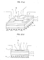
- Fig. 1 (a) and Fig. 1 (b) illustrate sensors according to a first embodiment of the present invention.
- the substrate 2 of the transistor 1A is made of insulating material.
- the silicon oxide layer of insulating and low-permittivity material (hereinafter, called “low-permittivity layer,” if necessary) 3 is formed on the upside (upper side in the Figs.) of the entire substrate.
- the source electrode 4 and the drain electrode 5, formed of gold are placed, between which the channel 6 formed with a carbon nano tube is bridged.
- the channel 6 is bridged between the source electrode 4 and the drain electrode 5 as if it were a bridge that connects the source electrode 4 and the drain electrode 5. Thereby it is apart from the low-permittivity layer 3 and the channel 6 is fixed to the transistor 1A at its two connecting points with the source electrode 4 and the drain electrode 5. The other portion of the channel 6 is in a state of being suspended in the air. Furthermore, as shown in FIG. 1 (b) , the channel 6 is bridged in a state of being bent at a predetermined angle.
- the channel 6 is bent at a predetermined angle to the extent that the compressive or tensile stress exerted upon the channel 6 can be absorbed, for example when the distance between the source electrode 4 and the drain electrode 5 is varied by the deformation of the substrate 2 by a temperature change.
- the channel 6 is set up to bent at a predetermined angle around the temperatures at which the sensor is used. Thereby it is able to absorb the stress caused by the themperature change in the neighborhood of the temperatures at which the sensor is used. But, in this embodiment, the channel 6 is set up to bent at a predetermined angle at room temperature.
- the side gate 7, formed of gold, is placed at the opposed position of the channel 6 on the low-permittivity layer 3.
- the side gate 7 is placed for applying a gate voltage to the channel 6.
- the source electrode 4, the drain electrode 5 and the side gate 7 are connected to an external power source, not shown in Figs., and are set up to be placed with a voltage by the external power source.
- the currents through the source electrode 4, the drain electrode 5 and the side gate 7 and the voltages applied to them are measured by a measuring instrument, not shown in Figs., respectively.
- the transistor 1A of this embodiment further comprises the back gate (the other gate) 9, as an interaction-sensing gate, formed of gold on the back side (lower side in the Figs.) of the entire substrate 2, or the opposite side to the low-permittivity layer 3.
- a specific substance (an antibody in the present embodiment) 10 that is capable of selectively interacting with the targets to be detected by the sensor of the present embodiment is immobilized on the back gate 9.
- the back gate 9 is set up not to be applied any voltages from outside.
- the most suitable gate voltage that the transfer characteristic of the transistor 1A shows the highest sensitivity will be tested to be found, by adjusting the gate voltage applied to the side gate 7.
- the most suitable gate voltage it will be set as the gate voltage applied to the side gate 7.
- the vicinity of the most suitable gate voltage means the range such that the change of the characteristic of the transistor is expected to reach the sufficient level on the detection of the detection targets.
- the electric potential of the back gate 9 will be canged by the interaction between the specific substance and the detection target, which leads to the change in the characteristic value of the transistor, such as the current value of the current between the souce electrode and the drain electrode, the threshold voltage or the gradient of the drain voltage to the gate voltage, or in the characteristic value peculiar to single-electron transistors, such as the threshold of Coulomb Oscillation, the Coulomb Oscillation period, the threshold of Coulomb Diamond or the Coulomb Diamond period.
- the characteristic value peculiar to single-electron transistors such as the threshold of Coulomb Oscillation, the Coulomb Oscillation period, the threshold of Coulomb Diamond or the Coulomb Diamond period.
- the transistor 1A can be set, using the side gate 7, in such a state that the transfer characteristic thereof shows the highest level in sensitivity, or that the transconductance thereof reaches the highest level.
- the influence given to the density change of the charged particles in the channel 6 by the change in the gate voltage, caused by the interaction between the specific substance and the detetion targets, can be maximized.
- the interaction between the specific substance and the detection targets can be measured as a large range of change in the characteristic of the transistor 1A. Consequently, the sensor according to the present embodiment can be set to be highly sensitive by amplifying the change in the characteristic of the transistor caused by the interaction between the specific substance and the detection targets.
- the detection targets can be detected with higer sensitivity.
- the limit of the detection sensitivity of a sensor using a transistor relates to the capacitance of the gate of the transistor (hereinafter, called "gate capacitance," if necessary).
- the gate capacitance is proportional to the product of the length of the channel L and the width W, or L x W, it is efficient to make the channel to be minute in order to reduce the gate capacitance. For these reasons, with a nano tube structure of this embodiment, which is extremely minute, detection targets can be detected with extremely high sensitivity.
- the back gate 9 is used as an interaction-sensing gate and antibody is immobilized on the back gate, high sensitivity detection can be performed with a simple construction. More specifically, because the back gate 9 is placed on the back side of the substrate 1A, the detection can be operated easily.
- the channel 6 is bridged between the source electrode 4 and the drain electrode 5 in a state of being bent, the risk of damage to the channel 6, induced by its deformation by temperature changes, can be reduced.
- the substrate 2 is an insulating substrate, the interaction at the back gate 9 can be surely detected.
- the low-permittivity layer 3 is formed between the channel 6 and the back gate (interaction-sensing gate) 9, the change in the surface charge caused by the interaction at the back gate 9 is transmitted more efficiently as a change of the electric charge density in the channel 6 and make itself shown as a large change in the characteristic of the transistor 1A. Consequently, the sensitivity of the sensor of the present embodiment is able to be highly enhanced.
- the use of the sensor of the present embodiment makes it possible to real-time measure, thereby the monitoring of the interaction between materials being realized.
- non-marker method immune sensors based on various principles such as surface plasmon resonance (SPR) have been developed, they have all been used as equipment for researches so not yet in practical use, for the lack of sufficient sensitivity fit for clinical-trial use. Also this immune sensor has a problem that the whole equipment is very upsized by the use of optical detection method.
- SPR surface plasmon resonance
- the senor of the present embodiment can achieve the advantages such as downsizing of the sensor, the rapidity of detection, the ease with operation, and so on.
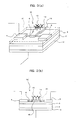
- Fig. 2 (a) and Fig. 2 (b) illustrate sensors according to a second embodiment of the present invention.
- the transistor 1B constructing the sensor of the second embodiment of the present invention has similar structure to the transistor 1A described in the first embodiment.
- the transistor 1B of the present embodiment further comprises the photosensitive resin layer of insulating and high-permittivity material (hereinafter, called "high-permittivity layer,” if necessary) 11 is formed on the upside of the entire low-permittivity layer 3.
- the high-permittivity layer 11 is formed to cover the whole channel 6, the lateral sides of the source electrode 4, the drain electrode 5 and the side gate 7 but not to cover the upsides (upper sides in Figs.) of the source electrode 4, the drain electrode 5 and the side gate 7.
- the high-permittivity layer 11 is shown by chain double-dashed line in Fig. 2 (a) and Fig. 2 (b).
- the sensor of the present embodiment is constructed as mentioned above, similar to the sensor of the first embodiment, it can be set in such a state that the transfer characteristic of the transistor 1B shows the highest level in sensitivity. Then, this makes it possible to measure the interaction between the specific substance and the detection targets as a wide range of change in the characteristic of the transistor 1B. Consequently, the sensor sensitivity of the present embodiment can be improved.
- the sensor can have higer sensitivity.
- the back gate 9 is used as an interaction-sensing gate, high sensitivity detection can be performed with simple construction and by simple operation.
- the substrate 2 is an insulating substrate, the interaction between the detection targets and the specific substance can be surely detected.
- the low-permittivity layer 3 is formed between the channel 6 and the back gate 9, the change in the surface charge caused by the interaction at the back gate 9 is transmitted to the channel 6 more efficiently, thereby the sensor sensitivity of the present embodiment can be further improved.
- the channel 6 is bent, the damage induced by the variation of length, caused by temperature changes or the like, can be prevented.
- photosensitive resin photoresist
- the high-permittivity layer 11 is filled around the channel 6, photosensitive resin (photoresist), which consists of the high-permittivity layer 11, is formed of material that is soft enough to allow deformation of the channel 6, thereby the damage can be prevented as mentioned above.
- the transfer characteristic of the transistor 1B can be more efficiently modulated by applying the gate voltage of the side date 7. Consequently, the sensitivity of the sensor is able to be further improved.
- the channel 6 is covered with the insulating and high-permittivity layer 11, leaking of the charged particles in the channel 6 to the outside thereof and intrusion of the charged particles to the channel 6 from outside of the channel 6, other than from the source electrode or the drain electrode, are able to be prevented. This results in that the interaction between the specific substance and detection targets can be detected steadily.
- the use of the sensor of the present embodiment makes it possible to real-time measure, thereby the monitoring of interaction between materials being realized. Further, it can be integrated easily, thereby a phenomenon of interaction between materials happened simultaneously in many places can be measured at a time.
- the senor of the present embodiment can achieve the advantages such as downsizing of the sensor, the rapidity of detection, the ease with operation, and so on.
- Fig. 3 (a) and Fig. 3 (b) illustrate sensors according to the third embodiment of the present invention.
- the transistor 1C constructing the sensors according to this embodiment similar to the first embodiment, comprises the substrate 2 fabricated with insulating material, the insulating and low-permittivity layer 3, the source electrode 4 and the drain electrode 5.
- the source electrode 4 and the drain electrode 5 are formed with gold.
- the channel 6 formed with a carbon nano tube is brdged between the source electrode 4 and the drain electrode 5.
- the back gate 12 for applying a gate voltage to the transistor 1C is formed on the back side of entire substrate 2.
- the back gate 12 is connected to a power supply, not shown in Figs., which applies a voltage to the back gate 12.
- the voltage placed to the back gate 12 is able to be measured with a measuring instrument, not shown in Figs.
- the membrane fabricated with silicon oxide (insulating membrane) 13 is formed, on the right side of the low-permittivity layer 3, from the middle of the channel 6 to the edge of the layer 3 in the depth direction in Figs.
- the channel 6 penetrates the insulating membrane 13 sideways. In other words, the portion around the middle of the channel 6 is covered with insulating membrane 13.
- the top gate 14 is formed of gold as an interaction-sensing gate.
- the top gate 14 is placed on the low-permittivity layer 3 with the insulating membrane 13 between them.
- the top gate 14 is constructed not to be applied with any voltage from outside. Further, the antibody 10 or the specific material is immobilized on the right side of the top gate 14.
- the insulator 21 is formed on the right side of the entire low-permittivity layer 3.
- the insulator 21 is formed to cover the portions of the channel 6 uncoverd with insulating membrane 13, the lateral sides of the source electrode 4, the drain electrode 5, the insulating membrane 13 and the top gate 14, but not to cover the upsides of the source electrode 4, the drain electrode 5 and the top gate 14.
- the insulator 21 is shown by chain double-dashed line in Fig. 3 (a) and Fig. 3 (b) .
- the sensor of the third embodiment of the present invention is constructed as mentioned above, similar to the sensor of the first embodiment, it can be set in such a state that the transfer characteristic of the transistor 1C shows the highest level in sensitivity. Then, this makes it possible to measure the interaction between the specific substance and the detection targets as a wide range of change in the characteristic of the transistor 1C. Consequently, the sensor sensitivity of the present embodiment can be improved.
- the senor can have higer sensitivity. Also, because the substrate 2 is an insulating substrate, the interaction between the detection targets and the specific substance can be surely detected.
- top gate 14 is used as an interaction-sensing gate, high sensitivity detection can be performed with simple construction and by simple operation.
- the low-permittivity insulating membarane 13 is formed between the channel 6 and the top gate 14, the change in the surface charge caused by the interaction at the top gate 14 is transmitted to the channel 6 more efficiently, thereby the sensor sensitivity of the present embodiment can be further improved.
- the channel 6 is covered with the insulator 21, leaking of the charged particles in the channel 6 to the outside thereof and intrusion of the charged particles to the channel 6 from outside of the channel 6, other than from the source electrode or the drain electrode, are able to be prevented. This results in that the interaction between the specific substance and detection targets can be detected steadily.
- the use of the sensor of the present embodiment makes it possible to measure real-time, thereby to be realized the monitoring of interaction between materials. Further, it can be integrated easily, thereby a phenomenon of interaction between materials happened simultaneously in many places can be measured at a time.
- the senor of the present embodiment can achieve the advantages such as downsizing of the sensor, the rapidity of detection, the ease with operation, and so on.
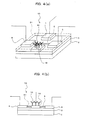
- Fig. 4 (a) and Fig. 4 (b) illustrate sensors according to a fourth embodiment of the present invention.
- the transistor 1D constructing the sensors according to this embodiment similar to the first embodiment, comprises the substrate 2 formed of insulating material, the insulating and low-permittivity layer 3, the source electrode 4 and the drain electrode 5.
- the source electrode 4 and the drain electrode 5 are formed of gold.
- the channel 6 formed with a carbon nano tube is bridged between the source electrode 4 and the drain electrode 5.
- the transistor 1D also comprises the side gate 7.
- the transistor 1D of the present embodiment further comprises the side gate 15 as an interaction-sensing gate on the opposite-side edge of low-permittivity layer 3 to the side gate 7, on the right side of which antibodies 10 are immobilized.
- the side gate 15 is constructed that in such a state that any voltages are not applied from the outside.
- the transistor 1D of the present embodiment also comprises the insulator 21 provided on the upside of the entire low-permittivity layer 3.
- the insulator 21 is formed to cover the whole channel 6, the lateral sides of the source electrode 4, the drain electrode 5 and the side gate 7, 15 but not to cover the upsides (upper sides in Figs.) of the source electrode 4, the drain electrode 5 and the side gate 7, 15.
- the insulator 21 is shown by chain, double-dashed line in Fig. 4 (a) and Fig. 4 (b) .
- the sensor of the present embodiment is constructed as mentioned above, similar to the sensor of the first embodiment, it can be set in such a state that the transfer characteristic of the transistor 1D shows the highest level in sensitivity. Then, this makes it possible to measure the interaction between the specific substance and the detection targets as a wide range of change in the characteristic of the transistor 1D. Consequently, the sensor sensitivity of the present embodiment can be improved.
- the sensor can have higer sensitivity. Also, because the side gate 15 is used as an interaction-sensing gate, high sensitivity detection can be performed with simple construction. Also, because the substrate 2 is an insulating substrate, the interaction between the detection targets and the specific substance can be surely detected.
- the channel 6 is covered with the insulating insulator 21, leaking of the charged particles in the channel 6 to the outside thereof and intrusion of the charged particles to the channel 6 from outside of the channel 6, other than from the source electrode 4 or the drain electrode 5, are able to be prevented. This results in that the interaction between the specific substance and detection targets can be detected steadily.
- the use of the sensor of the present embodiment makes it possible to measure real-time, thereby to be realized the monitoring of interaction between materials. Further, it can be integrated easily, thereby a phenomenon of interaction between materials happened simultaneously in many places can be measured at a time.
- the senor of the present embodiment can achieve the advantages such as downsizing of the sensor, the rapidity of detection, the ease with operation, and so on.
- Fig. 5 (a) and Fig. 5 (b) illustrate sensors according to the fifth embodiment of the present invention.
- the transistor 1E of the fifth embodiment of the present invention has similar constrction to the transistor 1A of the first embodiment, other than that it does not comprise the back gate 9 and the antibodies 10.
- the substrate 2 of the transistor 1A is fabricated with insulating material.
- the silicon oxide layer (low-permittivity layer) 3 of insulating and low-permittivity material is formed on the upside (upper side in the Figs.) of the entire substrate 2.
- the source electrode 4 and the drain electrode 5, formed with gold are placed, between which the channel 6 formed with a carbon nano tube is bridged.
- the channel 6 is bridged between the source electrode 4 and the drain electrode 5 as if it were a bridge that connects the source electrode 4 and the drain electrode 5, thereby it is apart from the low-permittivity layer 3.
- the channel 6 is fixed to the transistor 1A at its two connecting points with the source electrode 4 and the drain electrode 5.
- the other portion of the channel 6 is in a state of being suspended in the air.
- the channel 6 is bridged in a state of being bent at a predetermined angle.
- the channel 6 is bent at a predetermined angle to the extent that the compressive or tensile stress exerted upon the channel 6 can be absorbed, for example when the distance between the source electrode 4 and the drain electrode 5 is varied with deformation of the substrate 2 by a temperature change.
- the channel 6 is adjusted to bent at a predetermined angle around the temperatures at which the sensor is used, thereby it is able to absorb the stress caused by the themperature change in the neighborhood of the temperatures at which the sensor is used.
- the channel 6 is set up to bent at a predetermined angle at room temperature.
- the side gate 7, formed with gold, is placed at the opposed position of the channel 6 on the low-permittivity layer 3.
- the side gate 7 is placed for applying a gate voltage to the channel 6.
- the source electrode 4, the drain electrode 5 and the side gate 7 are connected to an external power source, not shown in Figs., and are set up to be placed with a voltage by the external power source.
- the transistor 1E of the present embodiment is constructed as mentioned above, owing to the fact that the channel 6 is bridged between the source electrode 4 and the drain electrode 5 in a state of being bent, the risk of damage to the channel 6, induced by its deformation by temperature changes, can be reduced even with a temperature change when it is used for detection or kept unused.
- the substrate 2 of the present embodiment is an insulating substrate, the permittivity of the substrate 2 can get lowered, which leads to the reduction in the gate capacitance, thereby the sensitivity of the transistor 1E can be enhanced.
- Fig. 6 (a) and Fig. 6 (b) illustrate sensors according to the sixth embodiment of the present invention.
- the transistor 1F of the sixth embodiment of the present invention has similar constrction to the transistor 1B of the second embodiment, other than that it does not comprise the back gate 9 and the antibodies 10.
- the transistor 1F constructing the sensor of the sixth embodiment of the present invention has similar structure to the transistor 1E described in the fifth embodiment.
- the transistor 1F of the present embodiment further comprises the photosensitive resin layer of insulating and high-permittivity material (high-permittivity layer) 11 is formed on the upside of the entire low-permittivity layer 3.
- the high-permittivity layer 11 is formed to cover the whole channel 6, the lateral sides of the source electrode 4, the drain electrode 5 and the side gate 7 but not to cover the upsides (upper sides in Figs.) of the source electrode 4, the drain electrode 5 and the side gate 7.
- the high-permittivity layer 11 is shown by chain double-dashed line in Fig. 6 (a) and Fig. 6 (b) .
- the sensor of the present embodiment is constructed as above-mentioned.
- the high-permittivity layer 11 a layer of high-permittivity and insulating material, is formed between the channel 6 and the side gate 7, the transfer characteristic of the transistor 1E can be more efficiently modulated by applying the gate voltage of the side date 7.
- the channel 6 is covered with the insulating and high-permittivity layer 11, leaking of the charged particles in the channel 6 to the outside thereof and intrusion of the charged particles to the channel 6 from outside of the channel 6, other than from the source electrode 4 or the drain electrode 5, are able to be prevented. This results in that the behavior of the transistor 1E can be stabled.
- the source electrode, drain electrode, gate, channel and interaction-sensing gate may be provided plurally.
- the transistor may be installed inside of an appropriate housing or installed on the other equipment.
- the sensor may not be immobilized with the specific substance thereon in the stage of manufacture or shipment, but the specific substance may be immobilized by a user. That is, it is to be understood that the embodiments of the sensors of the present invention may include those that are not immobilized with specific substances thereon.
- top gate, side gate and back gate have been used as an interaction-sensing gate in the above embodiments, it is needless to say that any other gate, as well as any other members than gates, may.be used as an interaction-sensing gate.
- channel 6 has been constructed to be bent in the above embodiments, of course it may not be bent but be straight.
- the channel 6 has been bridged between the source electrode 4 and the drain electrode 5 in the above embodiments, it may be provided being touched with the substrate 2 or the low-permittivity layer 3, for example. As far as the channel 6 is bent, even in a state where it is touched with the substrate 2 or the low-permittivity layer 3, the risk of damage to it caused by temperature changes can be reduced.
- a voltage can be applied on the interaction-sensing gate.
- transistor in the above embodiments means either the field-effect transistor or the single-electron transistor.
- a field-effect transistor and a single-electron transistor are the same in their basic structure, while the channels, which form current pathes, of them are different. More specifically, the channel of the single-electron transistor has a quantum dot structure and the channel of the field-effect transistor does not. Thus, they can be distinguished in the form of their consruction by the existence of a quantum dot structure.
- a substrate (indicated by the numeral reference 2 in the above embodiments), those made of any materials may be used as far as they are insulating substrates or insulated semiconductor substrates, without any other restriction. But it is preferred to be insulating substrates or substrates with its surfaces coverd with the material used for the insulating substrates, when they are used in sensors. When an insulating substrate is used, floating capacitance can be reduced because the permittivity of an insulating substrate is lower compared to the semiconductor substrate. Thereby, the detection sensitivity to detect the interaction with can be improved when a back gate is used as the interaction-sensing gate.
- An insulating substrate is a substrate formed with an insulator, which means an electric insulator as far as it is not specifically mentioned in the present specification.
- Examples of the insulator that forms the insulating substrate are silicon oxide, silicon nitride, aluminum oxide, titanium oxide, calcium fluoride, acrylic resin, polyimide resin, Teflon (registered trademark), etc. These examples may used in any kinds of combination with any percentage of each.
- a semiconductor substrate is a substrate formed with semiconductors.
- the semiconductor that forms the semiconductor substrate are silicon, gallium arsenide, gallium nitride, zinc oxide, indium phosphide, silicon carbide, etc. These examples may used in any kinds of combination with any percentage of each.
- examples of the insulator that forms the insulating membarane are the same as those used for the insulator that forms the above-mentioned insulating substrate.
- the semiconductor substrate can also work as a gate described below.
- the shape of the substrate is not limited particularly. But it is usually manufactured in the form of a plate.
- the size of the substrate is not restricted, either. But it is preferred to be more than 100 micrometers so as to maintain its mechanical strength.
- a source electrode (indicated by the numeral reference 4 in the above embodiments), there is no restrictions as far as it is an electrode that can supply carriers of the above-mentioned transistors.
- a drain electrode (indicated by the numeral reference 5 in the above embodiments), there is no restrictions either as far as it is an electrode that can receive carriers of the above-mentioned transistors.
- the source electrode as well as the drain electrode may be formed of any electric conductors. Examples thereof are gold, platinum, titanium, titanium carbide, tungsten, aluminum, molybdenum, chromium, tungsten silicide, tungsten nitride, polycrystal silicon, or the like. These examples may used in any kinds of combination with any percentage of each.
- a gate is usually constructed to have a conductor insulated from the channel and generally consisted of a conductor and an insulator.
- Examples of conductors forming gates are gold, platinum, titanium, titanium carbide, tungsten, tungsten silicide, tungsten nitride, aluminum, molybdenum, chromium, polycrystal silicon, etc. These examples may used in any kinds of combination with any percentage of each.
- the location of the gate has no restrictions as far as the gate voltage can be applied to the channel.
- it may be installed as a top gate which is upward to the substrate, as a side gate on the same surface as the channel of the substrate or as a back gate on the back side of the substrate.
- the top gate and the side gate may be formed on the surface of the channel with an insulating membrane between them.
- an insulating membrane there is no restriction as far as it is an insulating material, of which examples are inorganic materials like silicon oxide, silicon nitride, aluminum oxide, titanium oxide, calcium fluoride, and polymer materials like acrylic resin, epoxy resin, polyimide, Teflon (registered trademark), etc.
- any types of members may be used as far as they are able to immobilize specific substances thereon that are capable of selectively interacting with the detection targets.
- the interaction-sensing gate can be called an immobilizing member.
- the interaction-sensing gate can be called a non voltage-applied type immobilizing member because it is preferred not to be applied with a voltage from outside.
- conductors, semiconductors or even insulators may be used as an interaction-sensing gate for example. But usually conductors are used for the interaction-sensing gate, as in the case of the source electrode and the drainelectrode.
- the interaction-sensing gate can be called an electrode-construction type member. Further, to consider that it is not applied with a voltage, too, it can also be called a non voltage-applied and electrode-construction type member.
- Examples of conductors forming the interaction-sensing gate are gold, platinum, titanium, titanium carbide, tungsten, tungsten silicide, tungsten nitride, aluminum, molybdenum, chromium, polycrystal silicon, etc.' These examples may used in any kinds of combination with any percentage of each.
- the gate without any gate voltage application in the transistor is used as an interaction-sensing gate.
- the top gate, side gate or back gate can be selected preferably. Among the three of them, especially the top gate or back gate can be selected preferably.
- the top gate as an interaction-sensing gate, the distance to the channel is generally smaller compared to two other gates and thus the sensitivity of the sensor can be enhanced.
- the back gate is used as an interaction-sensing gate, the specific substance can be immobilized on the interaction-sensing gate easily.
- the channel (indicated by the numeral reference 6 in the above embodiments) may form a current path between the source electrode and the drain electrode. Any known types of channels can be used, if necessary.
- the channel is preferred to be passivated or protected with the cover of insulating materials.
- insulating materials can be used as the insulating cover. Examples of them are polymer materials like photoresist (photosensitive resin), acrylic resin, epoxy resin, polyimide, Teflon (registered trademark), and self-organizing membrane like aminopropylethoxysilane, lubricants like PER-fluoropalyether, Fonbrin (trade name), fullerene compound, or inorganic materials like silicon oxide, fluosilicate glass, HSQ (Hydrogen Silsesquioxane), MSQ (Methyl Lisesquioxane), porous silica, silicon nitride, aluminum oxide, titanium oxide, calcium fluoride, daiamond thin film, etc. These examples may used in any kinds of combination with any percentage of each.
- an insulating and low-permittivity layer is formed between the interaction-sensing gate and the channel.
- the portion between the interaction-sensing gate and the channel has preferably low-permittivity characteristic all over (that is, over all of the layers between the interaction-sensing gate and the channel).
- low-permittivity means that the relativedielectricconstant thereof is smaller than 4.5.
- any insulating and low-permittivity materials can be used to construct the low-permittivity layer, as mentioned above, without any other restrictions.
- examples thereof are inorganic materials like silicon dioxide, fluosilicate glass, HSQ (Hydrogen Silsesquioxane), MSQ (Methyl Lisesquioxane), porous silica, daiamond thin film, and organic materials like polyimide, Parylene-N, Palylene-F, polyimide fluoride, etc. These examples may used in any kinds of combination with any percentage of each.
- the portion between the channel and the interaction-sensing gate is insulating and low in permittivity, the change of the surface charge on the interaction-sensing gate can be transmitted more efficientoly in the form of the density change of the surface chaege in the channel.
- the above-mentioned interaction can be detected as a wide range of change in the output characteristic of the transistor and thus the sensitivity of the sensor can be further improved when the above-mentioned transistor is used as the sensor.
- an insulating and high-permittivity layer is formed between the gate for applying a voltage to the transistor and the channel.
- the portion between the gate and the channel has preferably high-permittivity characteristic all over (that is, over all of the layers between the gate and the channel).
- high-permittivity means that the relativedielectricconstant thereof is bigger than 4.5.
- any insulating and high-permittivity materials can be used to construct the high-permittivity layer, as mentioned above, without any other restrictions.
- examples thereof are inorganic materials like silicon nitride, aluminum oxide, tantalum oxide, and polymer materials with high-permittivity characteristic. These examples may used in any kinds of combination with any percentage of each.
- the transfer characteristic of the transistor can be modulated more efficiently with application of gate voltage.
- the sensitivity of the sensor can be further improved when the above-mentioned transistor is used as the sensor.
- the channel of the field-effect transistor (hereinafter, called “FET channel”, when necessary) and the channel of the single-electron transistor (hereinafter, called “SET channel”, when necessary) are explained respectively.
- the field-effect transistor and the single-electron transistor can be distinguished by the channel of each, as mentioned earlier.
- a transistor should be recognized as a field-effect transistor when it has a FET channel, and as a single-electron transistor when it has a SET channel.
- the FET channel may form a current path and any known channels can be used, if necessary. But the size of it is preferred to be minute.
- the nano tube structure is a structure shaped like a tube, whose size is 0.4 to 50 nm in diameter of the cross section orthogonal to the longitudinal direction.
- a shape like a tube means a shape with the ratio between the longitudinal length and the longest orthogonal length among all directions is in the range of 10 to 10000. It also includes shapes such as a rod (almost circular in its cross section) or a ribbon (flat and almost square in its cross section).
- a nano tube structure can be used as an electric charge transporter. Because it has a structure of one-dimensional quantum wire with several nano meters in diameter, the gate capacitance gets remarkably lowered compared to the field-effect transistors used in conventional sensors. Consequently, the change in the electric potential of the gate, caused by the interaction between the specific substance and the detection targets, gets extremely large. The change in the density of the charged particles existing in the channel gets extremely large, too. Thereby, the sensitivity of the detection for detecting targets is dramatically improved.
- nano tube structure examples include a carbon nano tube (CNT), a boron nitride nano tube and a titania nano tube.
- CNT carbon nano tube
- boron nitride nano tube boron nitride nano tube
- titania nano tube a carbon nano tube
- the detection sensitivity of the sensor has been restricted because of the difficulty in forming 10-nanometer class channel.
- the use of these nano tube structures makes it possible to form channels that are minuter than was previously possible.
- a nano tube structure shows an electrical property like either a semiconductor or a metal, depending on its chirality. When it is used as an FET channel like a semiconductor, it is preferred that it has an electrical property like a semiconductor.
- the SET channel may also form a current path similarly to the FET channel and any known channels can be used, if necessary.
- the size of it is also preferred to be minute.
- a nano tube structure may be used as an SET channel and examples of the nano tube structure are a carbon nano tube (CNT), a boron nitride nano tube and a titania nano tube or the like.
- the SET channel is different from the FET channel in the point that it has a quantum dot structure.
- any known materials with quantum dot structures can be used as SET channels, usually carbon nano tubes introduced with defects therein are used. More specifically, usually a cabon nano tube with 0.1 to 4 nanometer quantum dot structures between the defects is used. It can be produced by a chemical process such as heating a carbon nano tube without any defects in gas atmosphere like hydrogen, oxygen or argon, or boiling it in acid solution
- a nano tube structure with quantum dot structures shows Coulomb Blockade phenomenon, which blocks the intrusion of electrons into the quantum dot structure, and thus a single-electron transistor can be realized by using that type of nano tube structure.
- the gate capacitance of conventional silicon base MOSFET metal-oxide semiconductor field-effect transistor
- the gate capacitance of the above-mentioned single-electron transistor with a nano tube structure introduced with the defects is about 10 -19 to 10 -20 F. That is, the gate capacitance of a single-electron transistor decreases by a factor of about ten thousand to one hundred thousand, compared to the conventional silicon base MOSFET.
- the change in the gate capacitance, as well as the change in the density of the charged particles in the channel can be extremely enlarged through the use of a single-electron transistor having a channel formed with the above-mentioned nano tube structure, compared to the conventional field-effect transistor without a nano tube structure.
- the detection sensitivity with which the detection targets are detected can be highly improved.
- the another point in which the SET channel is different from the FET channel is that the nano tube structure used as the SET channel is preferred to have the electric property like metals.
- Examples of methods to check if the nano tube structure is like a metal or a semiconductor are the one with which the chirality of the carbon nano tube is determined by Raman spectroscopy or the other with which the electronic state density of the carbon nano tube is measured using scanning tunneling microscope (STM) spectroscopy.
- the detection target is not restricted particularly but any materials can be used.
- any types of materials may be used as far as they are capable of selectively interacting with the detection targets, without any other restriction. They may be, for example, enzyme, antibody, protein like lectin, peptide, hormone, nucleic acid, sugar, oligosaccharide, sugar chain like polysaccharide, lipid, low molecular compound, organic materials, inorganic materials, or fusion of these materials, and virus, cell, body tissue, or materials composing them, etc.
- the protein may be of its full length or may be a partial peptide including a binding activity portion.
- the protein with its amino-acid sequence and fuction known, as well as unknown may be used.
- synthesized peptide chain, proteins refined from an organism or proteins translated and refined from cDNA library or the like using appropriate translation system can be used as the target molecules.
- the synthesized peptide chain may be bound with sugar chain to be a glycoprotein.
- the synthesized protein with its amino-acid sequence known or the protein translated and refined from cDNA library or the like using appropriate process are preferably used.
- the nucleic acid is not limited particularly, and DNA as well as RNA can be used.
- the nucleic acid with its base sequence or fuction known, as well as unknown, may be used.
- the nucleic acid with its fuction that it has binding capacity in its protein and its base sequence known or the nucleic acid cut and isolated from genome library or the like using restricted enzyme and the like are preferably used.
- the sugar chain with its sugar sequence or fuction known, as well as unknown, may be used.
- the sugar chain that is already isolated and analyzed thus with its sugar sequence or fuction known is preferably used.
- the low-molecular compound is not limited particularly, as far as it is capable of interaction.
- the low molecular with its function unknown, as well as with its capability of bonding or reacting with proteins already known, can be used.
- the interaction-sensing gate immobilized specific materials thereon is suitably used for a biosensor used for detection of materials interacting with the functional material.
- the material, which interacts with the material already interacted with the specific substance can be marked by enzyme, by materials showing electrochemical reaction or luminous reaction, or by polymer and particles with electric charge.
- the “interaction” between the specific substance and the detection target is not limited particularly, but usually means the action caused by the force acting between the molecules that are combined with at least one type of combinations including covalent bond, hydrophobic bond, hydrogen bond, van der Waals binding or the combination made by electrostatic force.
- the covalent bond may include coordinate bond and dipolar coupling.
- the combination made by electrostatic force includes electrostatic repulsion, as well as electrostatic binding.
- the interaction includes reactions occured by the above-mentioned action, such as binding reaction, synthetic reaction or decomposition reaction.
- Examples of the interactions are: binding and dissociation between antigen and antibody, binding and dissociation between protein receptor and ligand, binding and dissociation between adhesion molecule and object molecule, binding and dissociation between enzyme and substrate, binding and dissociation between apoenzyme and coenzyme, binding and dissociation between nucleic acid and protein to be bound thereto, binding and dissociation between nucleic acids, binding and dissociation between proteins in communication system, binding and dissociation between glycoprotein and protein, binding and dissociation between sugar chain and protein, binding and dissociation between cells or body tissues and protein, binding and dissociation between cells or body tissues and low molecule compounds, interaction between ion and ion-sensitive material or the like.
- interaction is not limited to these types of actions, but also includes: immunoglobulin or the derivation F(ab') 2 , Fab', Fab, receptor or enzyme and the derivation thereof, nucleic acid, native and artificial peptide, artificial polymer, carbohydrate, lipid, inorganic material or organic ligand, virus, cell, drug and the like.
- the other examples of the "interaction" between the-specific substance immobilized on the interaction-sensing gate and the other material can include the response, related to the functional material immobilized on the gate, not to any substances but to the change in outside emvironments such as pH, ion, temperature, pressure or the like.
- the transistor using a carbon nano tube is produced according to the following procedure.
- the carbon nano tube used in the transistor shoud be manufactured controlling its position and orientation.
- it is usually produced using patterned catalyst with a method like photolithography, controlling its position and orientation.
- a carbon nano tube is produced according to the following steps.
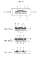
- Step 1 Patterning Photoresist 16 on the Substrate 2, as shown in Fig. 7 (a)
- the pattern corresponding to the position and the orientation where the carbon nano tube will be formed is determined. Then, the photoresist 16 is patterned according to the determined pattern on the substrate 2.
- Step 2 Evaporation Metal Catalyst 17, as shown in Fig. 7 (b)
- a metal that will be catalyst 17 is evaporated onto the patterend substrate 2.
- the metal to be catalyst 17 are transition metals like iron, nickel or cobalt, the alloys of them, etc.
- Step 4 Feed the Gas like Methane Gas or Alcohol Gas in CVD (chemical vapor deposition) furnace 18 at high temperature and forming carbon nano tube 19 between the Catalysts 17, as shown in Fig. 7 (d)
- metallic catalyst 17 turns to be minute particles of several nanometers in diameter, which is used as the core around which the carbon nano tube grows.
- the high temperature usually means from 300 to 1200 °C.
- the source electrode and the drain electrode are produced at the both edge of the carbon nano tube 19.
- ohmic electrodes are formed as the source electrode and the drain electrode.
- the source electrode and the drain electrode can be installed at the tips of the carbon nano tube 19 or at the lateral side thereof.
- the heat treatment in the range of 300 to 1000 °C can be made when the source electrode and the drain electrode are formed so as to get the improved condition of the electrical connections.
- the gate and the interaction-sensing gate are provided at appropriate positions, to finish the production of the transistor.
- the transistor can be produced forming the carbon nano tube 19 under control of the position and the orientation thereof.
- the probability of forming the carbon nano tube 19 between the catalyst metals is small by above-mentioned method of production (about 10 % in the test performed by the present inventors). So, as shown in Fig. 8 , the shape of the catalysts 17 are made to be pointed sharply and an electric charge is applied between the two catalysts while the carbon nano tube 19 is growing. This raises expectations that the carbon nano tube 19 grows between the sharp catalysts along the electrical flux line.
- the carbon nano tube 19 grows when an electric charge is applied between the catalysts 17 is not yet understood. However, the following two reasons are guessed. One is that the carbon nano tube 19, starting to grow from the electrode (catalyst 17, in this example), has large polarization moment and thus it grows along the direction of the electric field. The other is that the carbon ions decomposited at high temperature form the carbon nano tube 19 along the electrical flux line.
- the spacer layer 20 of silicon oxide or the like betweem the catalyst 17 and the substrate 2, as shown in Fig. 9 , which can make the carbon nano tube 19 apart from the substrate 2 during the growth thereof.
- the field-effect transistor can be produced.
- the single-electron transistor can be manufactured from the field-effect transistor by chemical treatings such as heating in atmosphere gas of hydrogen, oxygen or argon, or boiling in the acid solution so as to introduce the defects for forming quantum dot structure therein.
- the method of immobilizing the specific substance to the interaction-sensing gate is not limited particularly, as far as the immobilization can be done with the method.
- the substance can be binded directly to the interaction-sensing gate by physical adsorption, or by a flexible spacer, which has an anchor portion to bind the substance, placed at the interaction-sensing gate in advance, for example.
- the flexible spacer When a metal is used for the interaction-sensing gate, the flexible spacer includes, preferably alkylene with structural formula (CH 2 ) n (n shows a natural number 1 to 30, preferably 2 to 30, more preferably 2 to 15).
- the thiol group or the disulfide group which forms an anchor portion suitable for adsorption of metals like gold, is preferably used for one end of the spacer molecule.
- One or more conneting portions that can bind the specific substance to be immobilized are preferably included in the other end of the spacer molecule, which points to the other directions than to the interaction-sensing gate.
- the connecting portion may be various reactive functional group such as amino group, carboxyl group, hydroxyl group, suximide group, and hapten or chelate such as biotin, biotin derivative, digoxin, digoxigenin, fluorescein, fluorescein derivative, theophylline, for example.
- the conductive polymer may be, for example, polypyrrole, polythiophene, polyaniline or the like.
- the hydrophilic polymer may be polymer without any electric charge such as dextran or polyethylene oxide, and may be polymer with electric charge such as polyacrylic acid or carboxyl methyl dextran.
- polymer with electric charge with the use of the polymer with opposite electric charge to the specific substance to be immobilized, the specific substance can be connected or supported utilizing electric charge enrichment effect (cited document: farumashia patent, Japanese Patent No. 2814639 ).
- an ion-sensitive membrane corresponding to the specific ion can be formed on the interaction-sensing gate.
- the enzyme immobilization membrane can be formed instead of or together with the ion-sensitive membrane. This results in that the detection target can be detected by means of measuring the product of enzyme, acted as a catalyst toward the detection target.
- An insulating membrane can be selected as the interaction-sensing gate, other than metals.
- the materials used for the insulating membrane are inorganic materials such as silicon oxide, silicon nitride, aluminum oxide, titanium oxide, calcium fluoride, and polymer such as acrylic resin, epoxy resin, polyimide resin, Teflon (registered trademark), etc.
- an ion-sensitive membrane can be formed on the insulating membrane, if necessary, corresponding to the respective ions to be detected.
- the enzyme immobilization membrane can be formed instead of or together with the ion-sensitive membrane.
- the sensor of the present invention can be used in any appropriate area. Specific examples are in the following.
- a sensor for clinical examination on blood, urine or the like pH, electrolyte, dissolved gas, organic materials, hormone, allergen, medication, antibiotic, activity of the enzymes, protein, peptide, mutagenic materials, cell of microorganism, blood cell, blood type, hemostasis, DNA analysis can be measured.
- examples of sensors to be considered are ion sensor, enzyme sensor, microorganism sensor, immune sensor, enzyme immune sensor, luminescent immune sensor, fungi count sensor, blood clotting electrochemical sensing and electrochemical sensor using various electrochemical reactions.
- the sensor of the present invention can be used in the measurement in vivo and in situ, for example an insertion-type microsensor mounted on a catheter, implantable microsensor or capsule-mounted type microsensor using medical capsule (cited document: Karube et al. "Development and practical application of Sensor," vol.30 No.1 Bessatsu Kagaku Kogyo 1986 ).
- An field-effect transistor with a carbon nano tube as the channel was produced like the following.
- the photoresist 16 was patterend by a photolithography method so as to form a carbon nano tube growth catalyst on the surface of the insulating layer 20 ⁇ Fig. 10(a) ⁇ .
- HMDS hexamethyldisilazane
- the photoresist microposit "S1818” manufactured by Shipley Far East Ltd. was spin coated under the same condition.
- the Si substrate 2 is baked on a hot plate under at the temperature of 90 °C for one minute. Then, the Si substrate 2 coated with photoresist 16 was dipped into monochlorobenzene and after that it was dried by nitrogen brow. Then it was baked in an oven at the temperature of 85 °C for five minutes. After the baking, it was exposured with a patterend enzyme using an aligner and then was developed for four minutes in developing agent ("AZ300MIF developer (2.38%)" manufactured by Clariant Co.). Then it was rinsed out with flowing water for three minutes and was dried by nitrogen brow.
- the Si, Mo and Fe catalyst 17 is deposited on the Si substrate 2 patterend with the photoresist 16 using an EB vacuum evaporation system in order for the thicknesses of Si, Mo and Fe to be 100 ⁇ , 100 ⁇ and 30 ⁇ respectively, with deposition rate of 1 ⁇ per second ⁇ Fig. 10 (b) ⁇ .
- the lift-off was done in acetone which is being boiled. Then it was washed by acetone, then by ethanol, and finaly by flowing water, each for three minutes, and was dried by nitrogen brow ⁇ Fig. 10(c) ⁇ .
- the Si substrate 2 patterend with the catalyst 17 was set in a CVD furnace and blowed with ethanol, bubbled with Ar, with the rate of 750 cc per minute and hydrogen with the rate of 500 cc per minute, at the temperature of 900°C for 20 minutes so as to make the carbon nano tube 19 grow, which will be the channel ( Fig. 11 ). In this process, heating up and cooling down are done with Ar being blowed at the rate of 1000 cc per minute.
- the photoresist 16 was patterend on the Si substrate 2 by a photolithography method, mentioned above, so as to product the source electrode, drain electrode and side gate ⁇ Fig. 12(a) ⁇ .
- Ti and then Au are deposited on the Si substrate'2, so as to form the source electrode 4, drain electrode 5 and side gate electrode 7, using an EB vacuum evaporation system with the thicknesses of Ti and Au to be 300 ⁇ and 3000 ⁇ respectively and with the deposition rates of 0.5 ⁇ and 5 ⁇ per second respectively ⁇ Fig. 12(b) ⁇ .
- the lift-off was done in acetone that is being boiled. Then it was washed by acetone, then by ethanol, and finaly by flowing water, each for three minutes, and was dried by nitrogen brow ⁇ Fig. 12(c) ⁇ .
- HMDS is spin coated on the right side of the Si substrate 2, so as to protect the elements, under the condition of 500 rpm for ten seconds, then 4000 rpm for 30 seconds. Then the above-mentioned photoresist was spin coated under the same condition. Then the photoresist was hardened in an oven at the temperature 110°C for 30 minutes so as to form a layer protecting the elements.
- the SiO 2 layer 20 on the back side of the Si substrate 2 was removed by dry etching using RIE (reactive ion etching) device.
- RIE reactive ion etching
- SF 6 reactive ion etching
- etching was done for six minutes in plasma with the RF power of 100 W.
- Pt and then Au are deposited on the Si substrate 2, so as to form the back gate electrode (interaction-sensing gate) 9, using an EB vacuum evaporation system with the thicknesses of Pt and Au to be 300 ⁇ and 2000 ⁇ respectively and with the deposition rates of 0.5 ⁇ and 5 ⁇ per second respectively ( Fig. 13 ).
- the layer protecting the elements formed on the Si substrate 2 was removed by being washed in acetone being boiled, then by acetone, ethanol, and finaly by flowing water each for three minutes.
- the photoresist was patterend, similarly to the photolithography method used for patterning the source electrode 4, drain electrode 5 and side gate electrode 7, onto the right side of the elements in the area without the source electrode 4, drain electrode 5 and side gate electrode 7, so as to form the channel protecting layer 16 ( Fig. 14 ).
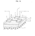
- the schematic diagram of the carbon nano tube - field effect transistor (hereinafter, called "CNT-FET" when necessary) produced by above-mentioned method is shown in Fig. 15 .
- the measurement of electric characteristic of CNT-FET was conducted using the semiconductor parameter analyzer 4156C manufactured by Agilent Co.
- the transfer characteristic (V SG - I SD characteristic) which is a kind of electric characteristic, was measured before and after the immobilization of the antibody and then the two measured values were compared.
- the result of the measurement is shown in Fig. 16 .
- the current that flows between the source electrode and the drain electrode (source drain current) I SD A was measured while the source voltage V S was maintained to 0 V and the drain voltage V D was sweeped -1 to 1 V (stepped by 0.02 V).
- the graph lines of negative in the value of source drain current indicates the measured value while V SD is -1.0 V and the graph lines of positive in the value of source drain current indicates the measured value while V SD is +1.0 V.
- the present invention can be applied to wide range of analysis such as chemical analysis, physical analysis or biological analysis, and is suitably used for a medical sensor or a biosensor for example.
Landscapes
- Chemical & Material Sciences (AREA)
- Engineering & Computer Science (AREA)
- Health & Medical Sciences (AREA)
- Life Sciences & Earth Sciences (AREA)
- Physics & Mathematics (AREA)
- Nanotechnology (AREA)
- Molecular Biology (AREA)
- General Physics & Mathematics (AREA)
- General Health & Medical Sciences (AREA)
- Analytical Chemistry (AREA)
- Biochemistry (AREA)
- Chemical Kinetics & Catalysis (AREA)
- Microelectronics & Electronic Packaging (AREA)
- Immunology (AREA)
- Pathology (AREA)
- Electrochemistry (AREA)
- Crystallography & Structural Chemistry (AREA)
- Spectroscopy & Molecular Physics (AREA)
- Condensed Matter Physics & Semiconductors (AREA)
- Materials Engineering (AREA)
- Composite Materials (AREA)
- Mathematical Physics (AREA)
- Theoretical Computer Science (AREA)
- Investigating Or Analyzing Materials By The Use Of Electric Means (AREA)
- Thin Film Transistor (AREA)
- Junction Field-Effect Transistors (AREA)
- Insulated Gate Type Field-Effect Transistor (AREA)
Applications Claiming Priority (2)
| Application Number | Priority Date | Filing Date | Title |
|---|---|---|---|
| JP2003307798A JP4669213B2 (ja) | 2003-08-29 | 2003-08-29 | 電界効果トランジスタ及び単一電子トランジスタ並びにそれを用いたセンサ |
| EP04772358A EP1666873A4 (fr) | 2003-08-29 | 2004-08-27 | Transistor a effet de champ, transistor a electron unique, et capteur associe |
Related Parent Applications (1)
| Application Number | Title | Priority Date | Filing Date |
|---|---|---|---|
| EP04772358A Division EP1666873A4 (fr) | 2003-08-29 | 2004-08-27 | Transistor a effet de champ, transistor a electron unique, et capteur associe |
Publications (2)
| Publication Number | Publication Date |
|---|---|
| EP2685251A2 true EP2685251A2 (fr) | 2014-01-15 |
| EP2685251A3 EP2685251A3 (fr) | 2014-03-05 |
Family
ID=34269461
Family Applications (2)
| Application Number | Title | Priority Date | Filing Date |
|---|---|---|---|
| EP20130181482 Withdrawn EP2685251A3 (fr) | 2003-08-29 | 2004-08-27 | Transistor à effet de champ, transistor à électron unique et capteur l'utilisant |
| EP04772358A Withdrawn EP1666873A4 (fr) | 2003-08-29 | 2004-08-27 | Transistor a effet de champ, transistor a electron unique, et capteur associe |
Family Applications After (1)
| Application Number | Title | Priority Date | Filing Date |
|---|---|---|---|
| EP04772358A Withdrawn EP1666873A4 (fr) | 2003-08-29 | 2004-08-27 | Transistor a effet de champ, transistor a electron unique, et capteur associe |
Country Status (7)
| Country | Link |
|---|---|
| US (4) | US8502277B2 (fr) |
| EP (2) | EP2685251A3 (fr) |
| JP (1) | JP4669213B2 (fr) |
| KR (1) | KR100746863B1 (fr) |
| CN (1) | CN100516854C (fr) |
| TW (1) | TWI261114B (fr) |
| WO (1) | WO2005022134A1 (fr) |
Families Citing this family (105)
| Publication number | Priority date | Publication date | Assignee | Title |
|---|---|---|---|---|
| TW200504359A (en) * | 2003-05-23 | 2005-02-01 | Japan Science & Tech Agency | Single-electron transistor, field-effect transistor, sensor, method for producing sensor, and sensing method |
| JP4669213B2 (ja) * | 2003-08-29 | 2011-04-13 | 独立行政法人科学技術振興機構 | 電界効果トランジスタ及び単一電子トランジスタ並びにそれを用いたセンサ |
| DE102004010635B4 (de) * | 2004-03-02 | 2006-10-05 | Micronas Gmbh | Vorrichtung zur Durchführung von Messungen an Biokomponenten |
| JP4360265B2 (ja) * | 2004-05-06 | 2009-11-11 | 株式会社日立製作所 | 生化学測定チップおよび測定装置 |
| US20080063566A1 (en) * | 2004-09-03 | 2008-03-13 | Mitsubishi Chemical Corporation | Sensor Unit and Reaction Field Cell Unit and Analyzer |
| WO2006103872A1 (fr) * | 2005-03-28 | 2006-10-05 | National University Corporation Hokkaido University | Transistor à effet de champ à nanotube de carbone |
| JP4742650B2 (ja) * | 2005-04-08 | 2011-08-10 | 東レ株式会社 | カーボンナノチューブ組成物、バイオセンサーおよびそれらの製造方法 |
| US7947485B2 (en) * | 2005-06-03 | 2011-05-24 | Hewlett-Packard Development Company, L.P. | Method and apparatus for molecular analysis using nanoelectronic circuits |
| WO2006134942A1 (fr) | 2005-06-14 | 2006-12-21 | Mitsumi Electric Co., Ltd. | Transistor à effet de champ, biocapteur en étant muni, et procédé de détection |
| KR100748408B1 (ko) * | 2005-06-28 | 2007-08-10 | 한국화학연구원 | 압타머를 이용한 탄소 나노튜브 트랜지스터 바이오센서 및이것을 이용한 타겟물질 검출 방법 |
| KR100653954B1 (ko) * | 2006-01-19 | 2006-12-05 | 한국표준과학연구원 | 나노전자소자 및 그 제조방법 |
| JP4935808B2 (ja) * | 2006-03-23 | 2012-05-23 | 富士通株式会社 | カーボンナノチューブデバイス及びその製造方法 |
| JP5076364B2 (ja) * | 2006-06-01 | 2012-11-21 | カシオ計算機株式会社 | 半導体センサ及び同定方法 |
| KR100863764B1 (ko) | 2006-07-07 | 2008-10-16 | 한국기계연구원 | 나노소재의 물리적 변형을 이용한 유동특성 검출방법 |
| JP5023326B2 (ja) * | 2006-09-28 | 2012-09-12 | 国立大学法人北海道大学 | 検出装置および検出方法 |
| US20100021993A1 (en) * | 2006-11-21 | 2010-01-28 | Ge Healthcare Bio-Sciences Corp. | System for assembling and utilizing sensors in containers |
| GB0801494D0 (en) | 2007-02-23 | 2008-03-05 | Univ Ind & Acad Collaboration | Nonvolatile memory electronic device using nanowire used as charge channel and nanoparticles used as charge trap and method for manufacturing the same |
| KR100888017B1 (ko) * | 2007-04-17 | 2009-03-09 | 성균관대학교산학협력단 | 극소량의 표적 물질 검출용 트랜지스터 기반 바이오센서 |
| EP2174122A2 (fr) * | 2007-06-08 | 2010-04-14 | Bharath R Takulapalli | Capteur d'effet de champ nano-structuré et ses procédés de formation et d'utilisation |
| EP2017609A1 (fr) * | 2007-07-18 | 2009-01-21 | Université Catholique de Louvain | Procédé et dispositif pour la détection quantitative et hautement sensible de molécules chimiques/biologiques |
| KR101478540B1 (ko) | 2007-09-17 | 2015-01-02 | 삼성전자 주식회사 | 트랜지스터의 채널로 나노 물질을 이용하는 바이오 센서 및그 제조 방법 |
| KR20090065272A (ko) | 2007-12-17 | 2009-06-22 | 한국전자통신연구원 | 바이오 센서 및 그 제조 방법 |
| US8297351B2 (en) * | 2007-12-27 | 2012-10-30 | Schlumberger Technology Corporation | Downhole sensing system using carbon nanotube FET |
| US20100053624A1 (en) | 2008-08-29 | 2010-03-04 | Kyung-Hwa Yoo | Biosensor |
| KR101118461B1 (ko) * | 2008-10-10 | 2012-03-06 | 나노칩스 (주) | 초고속 고감도 dna 염기서열 분석 시스템 |
| FR2943787B1 (fr) * | 2009-03-26 | 2012-10-12 | Commissariat Energie Atomique | Micro-dispositif de detection in situ de particules d'interet dans un milieu fluide, et procede de mise en oeuvre |
| US20100256518A1 (en) * | 2009-04-01 | 2010-10-07 | Yu Chris C | Micro-Devices for Biomedical Applications and Method of Use of Same |
| US8373153B2 (en) * | 2009-05-26 | 2013-02-12 | University Of Seoul Industry Cooperation Foundation | Photodetectors |
| US8367925B2 (en) * | 2009-06-29 | 2013-02-05 | University Of Seoul Industry Cooperation Foundation | Light-electricity conversion device |
| US8748862B2 (en) | 2009-07-06 | 2014-06-10 | University Of Seoul Industry Cooperation Foundation | Compound semiconductors |
| US8395141B2 (en) | 2009-07-06 | 2013-03-12 | University Of Seoul Industry Cooperation Foundation | Compound semiconductors |
| US8227793B2 (en) | 2009-07-06 | 2012-07-24 | University Of Seoul Industry Cooperation Foundation | Photodetector capable of detecting the visible light spectrum |
| US8809834B2 (en) | 2009-07-06 | 2014-08-19 | University Of Seoul Industry Cooperation Foundation | Photodetector capable of detecting long wavelength radiation |
| US8368990B2 (en) | 2009-08-21 | 2013-02-05 | University Of Seoul Industry Cooperation Foundation | Polariton mode optical switch with composite structure |
| US8368047B2 (en) * | 2009-10-27 | 2013-02-05 | University Of Seoul Industry Cooperation Foundation | Semiconductor device |
| US8058641B2 (en) | 2009-11-18 | 2011-11-15 | University of Seoul Industry Corporation Foundation | Copper blend I-VII compound semiconductor light-emitting devices |
| US9103773B2 (en) * | 2010-05-06 | 2015-08-11 | Seoul National University R&D Foundation | Capacitive element sensor and method for manufacturing same |
| KR101160585B1 (ko) * | 2010-07-30 | 2012-06-28 | 서울대학교산학협력단 | 탄소나노튜브를 게이트로 이용한 트랜지스터 및 그 제조방법 |
| US9880126B2 (en) * | 2010-09-24 | 2018-01-30 | Ajou University Industry-Academic Cooperation Foundation | Biosensor based on carbon nanotube-electric field effect transistor and method for producing the same |
| CN103649739B (zh) | 2011-05-05 | 2015-07-08 | 格拉芬斯克公司 | 使用石墨烯的用于化学传感的场效应晶体管、使用晶体管的化学传感器和制造晶体管的方法 |
| US8551833B2 (en) * | 2011-06-15 | 2013-10-08 | International Businesss Machines Corporation | Double gate planar field effect transistors |
| KR101774480B1 (ko) | 2011-08-16 | 2017-09-04 | 에레즈 할라미 | 전계 효과 트랜지스터의 비접촉 제어를 위한 방법 및 장치 그리고 두 개의 전자 장치들을 상호연결하는 방법 |
| KR101320687B1 (ko) * | 2011-10-04 | 2013-10-18 | 한국과학기술원 | 전계효과 트랜지스터를 이용한 바이오센서 |
| US8940235B2 (en) * | 2011-10-04 | 2015-01-27 | Samsung Electronics Co., Ltd. | Thin-film transistors for chemical sensor applications |
| US8629010B2 (en) * | 2011-10-21 | 2014-01-14 | International Business Machines Corporation | Carbon nanotube transistor employing embedded electrodes |
| KR101926356B1 (ko) | 2011-12-06 | 2018-12-07 | 삼성전자주식회사 | 백-바이어스 영역을 갖는 반도체 소자 |
| JP5898969B2 (ja) * | 2012-01-18 | 2016-04-06 | 株式会社日立製作所 | 半導体装置 |
| CA2862468A1 (fr) | 2012-01-23 | 2013-08-01 | The Ohio State University | Dispositifs et procedes permettant de detecter rapidement et precisement les substances a analyser |
| US9341592B2 (en) | 2012-04-09 | 2016-05-17 | Bharath Takulapalli | Field effect transistor, device including the transistor, and methods of forming and using same |
| FR2992774B1 (fr) * | 2012-06-29 | 2015-12-25 | Inst Nat Sciences Appliq | Capteur de molecule integrable dans un terminal mobile |
| US8906215B2 (en) | 2012-11-30 | 2014-12-09 | International Business Machines Corporation | Field effect based nanosensor for biopolymer manipulation and detection |
| US20140243214A1 (en) * | 2013-02-26 | 2014-08-28 | Hitachi, Ltd. | Fet array substrate, analysis system and method |
| US9331293B2 (en) * | 2013-03-14 | 2016-05-03 | Nutech Ventures | Floating-gate transistor photodetector with light absorbing layer |
| KR102050502B1 (ko) | 2013-03-18 | 2020-01-08 | 삼성전자주식회사 | 하이브리드 수직 공진 레이저 및 그 제조방법 |
| WO2014191892A1 (fr) * | 2013-05-29 | 2014-12-04 | Csir | Transistor à effet de champ et détecteur de gaz comprenant une pluralité de transistors à effet de champ |
| EP3026014A4 (fr) | 2013-07-25 | 2017-03-29 | Toray Industries, Inc. | Composite à base de nanotubes de carbone, dispositif semi-conducteur, et capteur les utilisant |
| US9355734B2 (en) * | 2014-03-04 | 2016-05-31 | Silicon Storage Technology, Inc. | Sensing circuits for use in low power nanometer flash memory devices |
| US20160054312A1 (en) | 2014-04-28 | 2016-02-25 | Nanomedical Diagnostics, Inc. | Chemically differentiated sensor array |
| EP2998737B1 (fr) | 2014-09-18 | 2021-04-21 | Nokia Technologies Oy | Appareil et procédé permettant de commander le chargement d'un canal avec des porteurs de charge, utilisant des points quantiques et le "Resonance Energy Transfer". |
| US9618474B2 (en) | 2014-12-18 | 2017-04-11 | Edico Genome, Inc. | Graphene FET devices, systems, and methods of using the same for sequencing nucleic acids |
| US11782057B2 (en) | 2014-12-18 | 2023-10-10 | Cardea Bio, Inc. | Ic with graphene fet sensor array patterned in layers above circuitry formed in a silicon based cmos wafer |
| US10020300B2 (en) | 2014-12-18 | 2018-07-10 | Agilome, Inc. | Graphene FET devices, systems, and methods of using the same for sequencing nucleic acids |
| CA2971589C (fr) * | 2014-12-18 | 2021-09-28 | Edico Genome Corporation | Transistor a effet de champ chimiquement sensible |
| US10006910B2 (en) | 2014-12-18 | 2018-06-26 | Agilome, Inc. | Chemically-sensitive field effect transistors, systems, and methods for manufacturing and using the same |
| US9859394B2 (en) | 2014-12-18 | 2018-01-02 | Agilome, Inc. | Graphene FET devices, systems, and methods of using the same for sequencing nucleic acids |
| US9857328B2 (en) | 2014-12-18 | 2018-01-02 | Agilome, Inc. | Chemically-sensitive field effect transistors, systems and methods for manufacturing and using the same |
| US12298301B2 (en) | 2014-12-18 | 2025-05-13 | Cardea Bio, Inc. | Chemically-sensitive field effect transistors, systems, and methods for manufacturing and using the same |
| US11921112B2 (en) | 2014-12-18 | 2024-03-05 | Paragraf Usa Inc. | Chemically-sensitive field effect transistors, systems, and methods for manufacturing and using the same |
| US10274455B2 (en) * | 2015-03-31 | 2019-04-30 | Rg Smart Pte. Ltd. | Nanoelectronic sensor pixel |
| US10107824B2 (en) * | 2015-04-20 | 2018-10-23 | National Tsing Hua University | Method for detecting cardiovascular disease biomarker |
| TWI591809B (zh) * | 2015-08-04 | 2017-07-11 | 國立交通大學 | 光感測裝置及其應用 |
| US10585062B2 (en) * | 2015-09-09 | 2020-03-10 | City University Of Hong Kong | Electrochemical detector |
| EP3176574B1 (fr) * | 2015-12-02 | 2021-01-27 | Emberion Oy | Détecteur et procédés associés |
| US10161901B2 (en) | 2015-12-07 | 2018-12-25 | Taiwan Semiconductor Manufacturing Co., Ltd. | Dual gate biologically sensitive field effect transistor |
| KR102480656B1 (ko) * | 2015-12-23 | 2022-12-23 | 한국재료연구원 | 듀얼 게이트 구조로 이루어진 유기 전계효과 트랜지스터 타입의 복합센서장치 및 그 제조방법 |
| WO2017184790A1 (fr) | 2016-04-19 | 2017-10-26 | Takulapalli Bharath | Capteur de nanopores, structure et dispositif comprenant le capteur, et procédés de formation et d'utilisation correspondants |
| US20190145926A1 (en) * | 2016-04-29 | 2019-05-16 | Stc. Unm | Wafer level gate modulation enhanced detectors |
| WO2017201081A1 (fr) * | 2016-05-16 | 2017-11-23 | Agilome, Inc. | Dispositifs à fet au graphène, systèmes et leurs méthodes d'utilisation pour le séquençage d'acides nucléiques |
| US10665799B2 (en) * | 2016-07-14 | 2020-05-26 | International Business Machines Corporation | N-type end-bonded metal contacts for carbon nanotube transistors |
| US10665798B2 (en) * | 2016-07-14 | 2020-05-26 | International Business Machines Corporation | Carbon nanotube transistor and logic with end-bonded metal contacts |
| CN106872531B (zh) * | 2017-01-23 | 2019-09-20 | 清华大学 | 场效应传感器及其制造方法 |
| KR101937157B1 (ko) | 2017-03-29 | 2019-01-11 | 재단법인 오송첨단의료산업진흥재단 | 플로팅 게이트 반도체 나노구조 바이오센서 및 이의 제조방법 |
| CN107328838B (zh) * | 2017-04-13 | 2019-11-05 | 南京大学 | 一种基于双栅极单电子晶体管的电子生物传感器及制备方法 |
| CN108732225B (zh) * | 2017-04-19 | 2021-07-13 | 中芯国际集成电路制造(上海)有限公司 | 离子敏感场效应晶体管及其形成方法 |
| EP3418729B1 (fr) * | 2017-06-22 | 2021-12-29 | Università degli Studi di Bari "Aldo Moro" | Capteur en forme de transistor à effet de champ |
| US20200256826A1 (en) * | 2017-10-27 | 2020-08-13 | Uwm Research Foundation, Inc. | Pulse-driven capacitive detection for field-effect transistors |
| TWI658268B (zh) * | 2017-11-29 | 2019-05-01 | 國立清華大學 | 血液檢測方法 |
| US10770546B2 (en) * | 2018-09-26 | 2020-09-08 | International Business Machines Corporation | High density nanotubes and nanotube devices |
| US10580768B1 (en) | 2018-09-28 | 2020-03-03 | Win Semiconductors Corp. | Gallium arsenide cell |
| KR102332792B1 (ko) * | 2019-05-10 | 2021-12-02 | 주식회사 엔디디 | 바이오 감지 장치 |
| KR102308171B1 (ko) * | 2019-05-10 | 2021-10-01 | 주식회사 엔디디 | 바이오 감지 장치 |
| KR102204591B1 (ko) | 2019-08-30 | 2021-01-19 | 권현화 | 나노바이오 감지 장치 |
| JP7336983B2 (ja) * | 2019-12-26 | 2023-09-01 | Tianma Japan株式会社 | イオンセンサ装置 |
| WO2021180958A1 (fr) | 2020-03-13 | 2021-09-16 | Quantum Motion Technologies Limited | Dispositif à points quantiques |
| CN115702343A (zh) * | 2020-07-03 | 2023-02-14 | 株式会社村田制作所 | 半导体传感器 |
| JP7487780B2 (ja) * | 2020-08-17 | 2024-05-21 | 株式会社村田製作所 | 半導体センサ |
| CN112697843B (zh) * | 2020-12-08 | 2023-10-03 | 湘潭大学 | 基于负电容效应的碳基场效应晶体管传感器 |
| TWI834132B (zh) * | 2021-06-22 | 2024-03-01 | 高熹騰 | 具有流體裝置的感測晶片 |
| TWI809715B (zh) * | 2022-02-15 | 2023-07-21 | 漢磊科技股份有限公司 | 用於生物晶片的結構 |
| TWI837599B (zh) * | 2022-02-25 | 2024-04-01 | 國立清華大學 | 具有選擇性的非酵素型感測元件及非酵素型感測器 |
| WO2023242297A1 (fr) * | 2022-06-15 | 2023-12-21 | Zhen Zhang | Dispositif de capteur de gaz à transistor à effet de champ |
| CN115274846B (zh) * | 2022-09-26 | 2023-01-10 | 晶通半导体(深圳)有限公司 | 高电子迁移率晶体管 |
| CN118191022B (zh) * | 2024-03-20 | 2025-03-25 | 北京大学 | 悬空阵列碳纳米管场效应晶体管生物传感器的制备方法 |
| CN119355091B (zh) * | 2024-12-27 | 2025-04-15 | 合肥美镓传感科技有限公司 | 气体传感器及其制备方法 |
| CN120129316B (zh) * | 2025-03-10 | 2025-11-21 | 西安电子科技大学 | 一种基于并联隧穿结垂直隧穿场效应晶体管的生物传感器及其制备方法 |
Family Cites Families (57)
| Publication number | Priority date | Publication date | Assignee | Title |
|---|---|---|---|---|
| US4180771A (en) * | 1977-12-02 | 1979-12-25 | Airco, Inc. | Chemical-sensitive field-effect transistor |
| JPS54161992A (en) | 1978-06-13 | 1979-12-22 | Asahi Glass Co Ltd | Immunity sensor and making method thereof |
| JPS57161541A (en) | 1981-03-31 | 1982-10-05 | Toshiba Corp | Ion sensor |
| JPS57191539A (en) | 1981-05-21 | 1982-11-25 | Nec Corp | Semiconductor ion sensor |
| SE431688B (sv) | 1981-07-30 | 1984-02-20 | Leif Lundblad | Anordning for utmatning av blad |
| JPS5928648A (ja) | 1982-08-11 | 1984-02-15 | Kuraray Co Ltd | 免疫濃度測定装置 |
| JPS6039547A (ja) | 1983-08-12 | 1985-03-01 | Mitsubishi Electric Corp | マルチ酵素センサ |
| JPS6047952A (ja) | 1983-08-26 | 1985-03-15 | Hitachi Ltd | 化学物質感応電界効果トランジスタ型センサ |
| JPS6189553A (ja) | 1984-10-08 | 1986-05-07 | Toyobo Co Ltd | 集積化酵素fet |
| JPH0646190B2 (ja) | 1985-08-14 | 1994-06-15 | 日本電気株式会社 | 半導体マルチバイオセンサ |
| JPS62132160A (ja) | 1985-12-04 | 1987-06-15 | Terumo Corp | 分離ゲ−ト型isfetを用いたバイオセンサ− |
| JPS62184345A (ja) | 1986-02-10 | 1987-08-12 | Toshiba Corp | イオン濃度の測定方法 |
| JPS62232556A (ja) | 1986-04-01 | 1987-10-13 | Kuraray Co Ltd | 免疫センサ及びその製造方法 |
| JPS62237347A (ja) * | 1986-04-08 | 1987-10-17 | Tokuyama Soda Co Ltd | 電界効果トランジスタ型ガスセンサ− |
| JPS6388438A (ja) | 1986-09-30 | 1988-04-19 | Shimadzu Corp | Mosfet化学電極 |
| JP2537354B2 (ja) | 1987-02-26 | 1996-09-25 | 新電元工業株式会社 | 半導体イオンセンサ |
| JPH0684951B2 (ja) | 1988-02-05 | 1994-10-26 | 生体機能利用化学品新製造技術研究組合 | 差動型半導体化学センサ |
| JPH01203959A (ja) | 1988-02-10 | 1989-08-16 | Fuji Photo Film Co Ltd | 酵素固定化fetセンサー |
| DE3827314C1 (fr) | 1988-08-11 | 1989-10-19 | Christoff Prof. Dr. Braeuchle | |
| SE8804074D0 (sv) * | 1988-11-10 | 1988-11-10 | Pharmacia Ab | Sensorenhet och dess anvaendning i biosensorsystem |
| JPH02280047A (ja) | 1989-04-21 | 1990-11-16 | Nec Corp | 1チップ半導体バイオセンサ |
| JPH0572979A (ja) | 1991-09-11 | 1993-03-26 | Nobuhisa Kawano | 移動する看板及びその装置 |
| GB2278235B (en) * | 1991-10-21 | 1996-05-08 | Holm Kennedy James W | Method and device for biochemical sensing |
| CN2160157Y (zh) * | 1993-05-21 | 1994-03-30 | 中国科学院半导体研究所 | 钯栅场效应晶体管 |
| JP3502135B2 (ja) | 1993-12-24 | 2004-03-02 | テルモ株式会社 | 血管内挿入用医療器具およびその製造方法 |
| JPH0894577A (ja) | 1994-09-22 | 1996-04-12 | Fujitsu Ltd | 半導体イオンセンサ及びその使用方法 |
| JPH08278281A (ja) | 1995-04-07 | 1996-10-22 | Hitachi Ltd | 電界効果型化学物質検出装置およびそれを用いたdna配列決定装置 |
| US5719033A (en) * | 1995-06-28 | 1998-02-17 | Motorola, Inc. | Thin film transistor bio/chemical sensor |
| US5827482A (en) | 1996-08-20 | 1998-10-27 | Motorola Corporation | Transistor-based apparatus and method for molecular detection and field enhancement |
| JPH10203810A (ja) | 1997-01-21 | 1998-08-04 | Canon Inc | カーボンナノチューブの製法 |
| JPH10260156A (ja) | 1997-03-18 | 1998-09-29 | Hitachi Ltd | センサー |
| US6287765B1 (en) * | 1998-05-20 | 2001-09-11 | Molecular Machines, Inc. | Methods for detecting and identifying single molecules |
| US6346189B1 (en) | 1998-08-14 | 2002-02-12 | The Board Of Trustees Of The Leland Stanford Junior University | Carbon nanotube structures made using catalyst islands |
| US7173005B2 (en) * | 1998-09-02 | 2007-02-06 | Antyra Inc. | Insulin and IGF-1 receptor agonists and antagonists |
| US6472705B1 (en) * | 1998-11-18 | 2002-10-29 | International Business Machines Corporation | Molecular memory & logic |
| JP2000187017A (ja) * | 1998-12-22 | 2000-07-04 | Matsushita Electric Works Ltd | 半導体イオンセンサ |
| US6815218B1 (en) * | 1999-06-09 | 2004-11-09 | Massachusetts Institute Of Technology | Methods for manufacturing bioelectronic devices |
| JP2001033423A (ja) | 1999-07-16 | 2001-02-09 | Horiba Ltd | 比較電極機能付イオン感応性電界効果トランジスタ型センサ |
| JP2003507889A (ja) * | 1999-08-18 | 2003-02-25 | ノース・キャロライナ・ステイト・ユニヴァーシティ | 化学的にゲート動作する単一電子トランジスタを使用したセンシングデバイス |
| WO2001044796A1 (fr) * | 1999-12-15 | 2001-06-21 | Board Of Trustees Of The Leland Stanford Junior University | Dispositifs de nanotubes de carbone |
| GB2364933B (en) * | 2000-07-18 | 2002-12-31 | Lg Electronics Inc | Method of horizontally growing carbon nanotubes |
| JP4140180B2 (ja) * | 2000-08-31 | 2008-08-27 | 富士ゼロックス株式会社 | トランジスタ |
| ATE408140T1 (de) * | 2000-12-11 | 2008-09-15 | Harvard College | Vorrichtung enthaltend nanosensoren zur ekennung eines analyten und verfahren zu ihrer herstellung |
| JP3867510B2 (ja) * | 2001-03-30 | 2007-01-10 | セイコーエプソン株式会社 | バイオセンサおよびその製造方法 |
| JP3883512B2 (ja) * | 2001-04-23 | 2007-02-21 | 三星電子株式会社 | 微細流路の側壁に形成されたmosfetよりなる物質検出用チップ、これを含む物質検出装置、及び物質検出装置を利用した物質検出方法 |
| JP3963686B2 (ja) | 2001-10-01 | 2007-08-22 | 富士通株式会社 | カーボンナノチューブゲート高電子移動度トランジスタ、及びその製造方法 |
| JP2003017508A (ja) | 2001-07-05 | 2003-01-17 | Nec Corp | 電界効果トランジスタ |
| US7385262B2 (en) * | 2001-11-27 | 2008-06-10 | The Board Of Trustees Of The Leland Stanford Junior University | Band-structure modulation of nano-structures in an electric field |
| US6835613B2 (en) * | 2001-12-06 | 2004-12-28 | University Of South Florida | Method of producing an integrated circuit with a carbon nanotube |
| US20040132070A1 (en) * | 2002-01-16 | 2004-07-08 | Nanomix, Inc. | Nonotube-based electronic detection of biological molecules |
| EP1348951A1 (fr) * | 2002-03-29 | 2003-10-01 | Interuniversitair Micro-Elektronica Centrum | Capteur formé par un transistor à effet de champ controllé par molécules et avec deux grilles |
| AU2003258969A1 (en) * | 2002-06-27 | 2004-01-19 | Nanosys Inc. | Planar nanowire based sensor elements, devices, systems and methods for using and making same |
| US7186380B2 (en) * | 2002-07-01 | 2007-03-06 | Hewlett-Packard Development Company, L.P. | Transistor and sensors made from molecular materials with electric dipoles |
| US7358121B2 (en) * | 2002-08-23 | 2008-04-15 | Intel Corporation | Tri-gate devices and methods of fabrication |
| WO2004094308A1 (fr) * | 2003-04-22 | 2004-11-04 | Commissariat A L'energie Atomique | Procede pour modifier au moins une propriete electrique d'un nanotube ou d'un nanofil et transistor incorporant celui-ci |
| JP4669213B2 (ja) * | 2003-08-29 | 2011-04-13 | 独立行政法人科学技術振興機構 | 電界効果トランジスタ及び単一電子トランジスタ並びにそれを用いたセンサ |
| JP2005285822A (ja) * | 2004-03-26 | 2005-10-13 | Fujitsu Ltd | 半導体装置および半導体センサ |
-
2003
- 2003-08-29 JP JP2003307798A patent/JP4669213B2/ja not_active Expired - Fee Related
-
2004
- 2004-08-27 EP EP20130181482 patent/EP2685251A3/fr not_active Withdrawn
- 2004-08-27 KR KR1020067004025A patent/KR100746863B1/ko not_active Expired - Fee Related
- 2004-08-27 CN CNB2004800246203A patent/CN100516854C/zh not_active Expired - Fee Related
- 2004-08-27 US US10/570,279 patent/US8502277B2/en not_active Expired - Fee Related
- 2004-08-27 WO PCT/JP2004/012402 patent/WO2005022134A1/fr not_active Ceased
- 2004-08-27 TW TW93125771A patent/TWI261114B/zh not_active IP Right Cessation
- 2004-08-27 EP EP04772358A patent/EP1666873A4/fr not_active Withdrawn
-
2012
- 2012-07-24 US US13/556,316 patent/US8766326B2/en not_active Expired - Fee Related
- 2012-07-24 US US13/556,314 patent/US8772099B2/en not_active Expired - Fee Related
-
2014
- 2014-06-12 US US14/302,842 patent/US9506892B2/en not_active Expired - Fee Related
Also Published As
| Publication number | Publication date |
|---|---|
| CN100516854C (zh) | 2009-07-22 |
| WO2005022134A1 (fr) | 2005-03-10 |
| US20120286763A1 (en) | 2012-11-15 |
| US8772099B2 (en) | 2014-07-08 |
| JP2005079342A (ja) | 2005-03-24 |
| US20070063304A1 (en) | 2007-03-22 |
| US9506892B2 (en) | 2016-11-29 |
| TWI261114B (en) | 2006-09-01 |
| EP1666873A4 (fr) | 2011-10-26 |
| KR100746863B1 (ko) | 2007-08-07 |
| KR20060036487A (ko) | 2006-04-28 |
| US20150102283A1 (en) | 2015-04-16 |
| EP1666873A1 (fr) | 2006-06-07 |
| CN1842704A (zh) | 2006-10-04 |
| JP4669213B2 (ja) | 2011-04-13 |
| EP2685251A3 (fr) | 2014-03-05 |
| US20120286243A1 (en) | 2012-11-15 |
| US8766326B2 (en) | 2014-07-01 |
| US8502277B2 (en) | 2013-08-06 |
| TW200519379A (en) | 2005-06-16 |
Similar Documents
| Publication | Publication Date | Title |
|---|---|---|
| US8502277B2 (en) | Field-effect transistor, single-electron transistor and sensor using the same | |
| US10401353B2 (en) | Systems and methods for single-molecule nucleic-acid assay platforms | |
| JP4775262B2 (ja) | センサユニット及び反応場セルユニット並びに分析装置 | |
| Noyce et al. | Electronic stability of carbon nanotube transistors under long-term bias stress | |
| CN111965231B (zh) | 一种用于病毒检测的半导体传感器及其制备方法与应用 | |
| US8017938B2 (en) | Apparatus for microarray binding sensors having biological probe materials using carbon nanotube transistors | |
| US8154093B2 (en) | Nano-electronic sensors for chemical and biological analytes, including capacitance and bio-membrane devices | |
| US7943394B2 (en) | Method and device for high sensitivity detection of the presence of DNA and other probes | |
| EP4241073A1 (fr) | Capteur comprenant des transistors à base de graphène | |
| US20110183438A1 (en) | Method for Sensing a Substance to be Detected in a Sample | |
| US20110193183A1 (en) | Nanowire sensor, nanowire sensor array and method of fabricating the same | |
| JP2023500818A (ja) | 全粒子ウイルス検出のための量子力学的トンネル電流センサである電気式センサ | |
| CN102016570A (zh) | 使用和构建纳米传感器平台的方法 | |
| US20080009002A1 (en) | Analyte Identification Using Electronic Devices | |
| JP2009002939A (ja) | アンペロメトリック型バイオセンサ | |
| JP2008286714A (ja) | ボルタノメトリック型バイオセンサ | |
| KR100746867B1 (ko) | 전계 효과 트랜지스터 및 단일 전자 트랜지스터 | |
| JP2009250633A (ja) | センサおよび検出方法 | |
| Sorgenfrei et al. | Single-molecule electronic detection using nanoscale field-effect devices | |
| Lee et al. | Silicon nanowires for high-sensitivity crp detection | |
| Cui et al. | Ultrasensitive and Selective Multiplexing Detection of Cancer Markers Using Nanowire Nanosensors |
Legal Events
| Date | Code | Title | Description |
|---|---|---|---|
| PUAI | Public reference made under article 153(3) epc to a published international application that has entered the european phase |
Free format text: ORIGINAL CODE: 0009012 |
|
| AC | Divisional application: reference to earlier application |
Ref document number: 1666873 Country of ref document: EP Kind code of ref document: P |
|
| AK | Designated contracting states |
Kind code of ref document: A2 Designated state(s): DE ES FR GB |
|
| PUAL | Search report despatched |
Free format text: ORIGINAL CODE: 0009013 |
|
| AK | Designated contracting states |
Kind code of ref document: A3 Designated state(s): DE ES FR GB |
|
| RIC1 | Information provided on ipc code assigned before grant |
Ipc: B82Y 30/00 20110101ALI20140129BHEP Ipc: G01N 27/414 20060101AFI20140129BHEP Ipc: B82Y 10/00 20110101ALI20140129BHEP |
|
| RIN1 | Information on inventor provided before grant (corrected) |
Inventor name: YAMADA, YUTAKA Inventor name: NAGAO, SATORU Inventor name: IFUKU, YASUO Inventor name: NAGAIKE, KAZUHIRO Inventor name: KOJIMA, ATSUHIKO Inventor name: MATSUMOTO, KAZUHIKO Inventor name: MITANI, HIROSHI Inventor name: KATOU, MASANORI |
|
| 17P | Request for examination filed |
Effective date: 20140828 |
|
| RBV | Designated contracting states (corrected) |
Designated state(s): DE ES FR GB |
|
| STAA | Information on the status of an ep patent application or granted ep patent |
Free format text: STATUS: THE APPLICATION HAS BEEN WITHDRAWN |
|
| 18W | Application withdrawn |
Effective date: 20161201 |