EP2685497A1 - Integrierter SOI-Schaltkreis, der eine seitliche Diode zum Schutz gegen elektrostatische Entladungen umfasst - Google Patents
Integrierter SOI-Schaltkreis, der eine seitliche Diode zum Schutz gegen elektrostatische Entladungen umfasst Download PDFInfo
- Publication number
- EP2685497A1 EP2685497A1 EP13175433.5A EP13175433A EP2685497A1 EP 2685497 A1 EP2685497 A1 EP 2685497A1 EP 13175433 A EP13175433 A EP 13175433A EP 2685497 A1 EP2685497 A1 EP 2685497A1
- Authority
- EP
- European Patent Office
- Prior art keywords
- circuit
- ground plane
- semiconductor
- zone
- transistor
- Prior art date
- Legal status (The legal status is an assumption and is not a legal conclusion. Google has not performed a legal analysis and makes no representation as to the accuracy of the status listed.)
- Withdrawn
Links
Images


Classifications
-
- H—ELECTRICITY
- H10—SEMICONDUCTOR DEVICES; ELECTRIC SOLID-STATE DEVICES NOT OTHERWISE PROVIDED FOR
- H10D—INORGANIC ELECTRIC SEMICONDUCTOR DEVICES
- H10D86/00—Integrated devices formed in or on insulating or conducting substrates, e.g. formed in silicon-on-insulator [SOI] substrates or on stainless steel or glass substrates
- H10D86/201—Integrated devices formed in or on insulating or conducting substrates, e.g. formed in silicon-on-insulator [SOI] substrates or on stainless steel or glass substrates the substrates comprising an insulating layer on a semiconductor body, e.g. SOI
-
- H—ELECTRICITY
- H10—SEMICONDUCTOR DEVICES; ELECTRIC SOLID-STATE DEVICES NOT OTHERWISE PROVIDED FOR
- H10D—INORGANIC ELECTRIC SEMICONDUCTOR DEVICES
- H10D87/00—Integrated devices comprising both bulk components and either SOI or SOS components on the same substrate
-
- H—ELECTRICITY
- H10—SEMICONDUCTOR DEVICES; ELECTRIC SOLID-STATE DEVICES NOT OTHERWISE PROVIDED FOR
- H10D—INORGANIC ELECTRIC SEMICONDUCTOR DEVICES
- H10D89/00—Aspects of integrated devices not covered by groups H10D84/00 - H10D88/00
- H10D89/60—Integrated devices comprising arrangements for electrical or thermal protection, e.g. protection circuits against electrostatic discharge [ESD]
- H10D89/601—Integrated devices comprising arrangements for electrical or thermal protection, e.g. protection circuits against electrostatic discharge [ESD] for devices having insulated gate electrodes, e.g. for IGFETs or IGBTs
- H10D89/611—Integrated devices comprising arrangements for electrical or thermal protection, e.g. protection circuits against electrostatic discharge [ESD] for devices having insulated gate electrodes, e.g. for IGFETs or IGBTs using diodes as protective elements
-
- H—ELECTRICITY
- H10—SEMICONDUCTOR DEVICES; ELECTRIC SOLID-STATE DEVICES NOT OTHERWISE PROVIDED FOR
- H10D—INORGANIC ELECTRIC SEMICONDUCTOR DEVICES
- H10D89/00—Aspects of integrated devices not covered by groups H10D84/00 - H10D88/00
- H10D89/60—Integrated devices comprising arrangements for electrical or thermal protection, e.g. protection circuits against electrostatic discharge [ESD]
- H10D89/601—Integrated devices comprising arrangements for electrical or thermal protection, e.g. protection circuits against electrostatic discharge [ESD] for devices having insulated gate electrodes, e.g. for IGFETs or IGBTs
- H10D89/931—Integrated devices comprising arrangements for electrical or thermal protection, e.g. protection circuits against electrostatic discharge [ESD] for devices having insulated gate electrodes, e.g. for IGFETs or IGBTs characterised by the dispositions of the protective arrangements
Definitions
- the invention relates to integrated circuits, and in particular integrated circuits made on a silicon-on-insulator (SOI) type substrate.
- SOI technology consists of separating a thin layer of silicon (a few nanometers) on a silicon substrate by a relatively thick insulating layer (a few tens of nanometers as a rule).
- Integrated circuits made in SOI technology have a number of advantages. Such circuits generally have lower power consumption for equivalent performance. Such circuits also induce lower parasitic capacitances, which make it possible to improve the switching speed. In addition, the phenomenon of latchup in the English language encountered by MOS transistors Bulk technology can be avoided. Such circuits are therefore particularly suitable for SoC or MEMS type applications. It can also be seen that the SOI integrated circuits are less sensitive to the effects of ionizing radiation and thus prove more reliable in applications where such radiations can induce operating problems, especially in space applications.
- the SOI integrated circuits can notably comprise SRAM-type random access devices or logic gates.
- LVT low threshold voltage transistors
- HVT high voltage threshold transistors
- SVT Standard V T " in English, typically 450mV
- RVT regular V T " in English
- the transistors are generally surrounded by insulation trenches (referred to by the acronym STI for "Shallow Trench Isolation" in English) which extend to below the caissons.
- STI Insulation trenches
- Such integrated circuits also include protection devices against electrostatic discharges (ESD for "Electrostatic Discharge” in English) accidental and can deteriorate these transistors.
- ESD electrostatic Discharge
- the document US2007 / 063284 describes an integrated circuit comprising an FDSOI transistor formed on an insulating layer of UTBOX type.
- a semiconductor ground plane is disposed beneath the buried insulating layer.
- a box is disposed under this ground plane.
- An isolation trench is provided at the periphery of the transistor through the insulating layer and extends into the box. Another isolation trench extends through the insulating layer, without reaching the box.
- a diode is provided on the side of the transistor from two opposite doping semiconductor regions and in contact with each other to form a diode.
- the device comprises a pn diode, formed on one side of the transistor and under the insulating layer.
- This pn diode comprises first and second semiconductor zones of opposite dopings, between which extends a third semiconductor zone of lower doping level.
- the first and second zones have electrical contacts respective, separated from each other by an insulation trench extending on the top of the insulating layer.
- This device nevertheless has certain disadvantages.
- the electrical performance of the diode is degraded by the presence of large leakage currents between the first and second semiconductor regions, which can affect the performance of the diode.
- the manufacturing processes typically employed only offer a reduced control of the width of the diode, which has the disadvantages, on the one hand, of limiting the number of such diodes that can be produced on a given surface of the diode. circuit, and secondly to restrict a control of electrical properties of said diode, such as breakdown voltage or leakage.
- the isolation trench is likely to be damaged during manufacturing steps of the integrated circuit.
- the manufacturing processes include steps of forming and removing insulating masks that are capable of structurally degrade side edges of said trench.
- the invention aims to solve one or more of these disadvantages.
- the invention thus relates to an integrated circuit as defined in the appended claims.
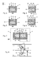
- the transistor 8 comprises a layer of a semiconductor material, called the active layer, formed on the insulating layer 10 and in line with this insulating layer 10. To simplify the drawings, the detailed structure of this active layer is not represented.
- This active layer may comprise, in a manner known per se, a channel of lightly doped semiconductor material, with a dopant concentration substantially equal to the dopant concentration of the substrate 18.
- the transistor 8 also comprises gate electrodes, source electrodes and electrodes. drain.
- the buried insulating layer 10 electrically isolates the transistor 8 from the ground plane 12, the box 14 and the substrate 18.
- the ground plane 12 is configured to be biased in voltage, typically via a control circuit not shown here.
- the polarization of the ground plane 12 makes it possible to control the threshold voltage of the transistor 8.
- the trench 16 is formed at the periphery of the transistor 8 and extends in depth through the insulating layer 10, as far as the box 14.
- the component 4 is able to protect the transistor 8 against electrostatic discharges that may occur on one or more electrodes of the transistor 8.
- the component 4 comprises a diode 20 with pn junction, formed on one side of the transistor 8 and separated from this transistor 8 by an isolation trench 21.
- This diode 20 comprises first 22 and second 24 semiconductor zones, having opposite types of doping. These zones 22 and 24 are coplanar with the plane of mass 12. By coplanar means that one can define a plane parallel to the layer 10 and passing through the zones concerned.
- the zone 22 is electrically connected to a first electrode E1 of the transistor 8.
- the zone 24 is electrically connected to a second electrode E2 of the transistor 8.
- the component 4 further comprises a second isolation trench 26, to separate between them the zones 22 and 24 of the diode 20.
- This trench 26 is formed of an electrically insulating material.
- This trench 26 extends through the insulating layer 10, into the ground plane 12 and to a depth strictly less than the interface between the ground plane 12 and the box 14.
- the depth under the insulating layer 10 is defined with respect to a plane extending along the interface separating the insulating layer 10 and the ground plane 12 and along a vertical direction, perpendicular to the direction of the plane of the substrate 18 .
- the component 4 also comprises a third semiconductor zone 28.
- This zone 28 extends under the trench 26 and forms a first semiconductor junction between the zones 22 and 24. This zone 28 allows the circulation of electric charge carriers between the zones 22 and 24.
- the diode 20 can be considered as planar, because of the presence of the semiconductor zones 22, 24 and 28 side by side in the same layer of the circuit .
- the trench 26 extends through the insulating layer 10 and under the insulating layer 10, while having a depth substantially less than that of the trench 16. This makes it possible to attenuate the appearance of leakage currents between the zones 22. and 24 and improve the electrical performance of the diode 20.
- the lateral dimension of such a trench 26 can be reduced.
- the lateral dimension of the trench 26 here designates the smallest distance separating the zones 22 and 24 from each other. This reduction of the lateral dimension makes it possible on the one hand to improve the control of certain electrical properties of the diode 20, such as the breakdown voltage, and on the other hand to reduce the space occupied by the circuit 2. In particular if the diode were made with an isolation trench provided on the insulating layer 10 without passing through the insulating layer 10, the lateral dimension of the isolation trench could not be so easily reduced without degrading the electrical performance of the diode.
- the trench 26 may have a lateral dimension of less than 70nm.
- the electrical performance of the diode 20 can be improved, in particular by limiting the transit time of charge carriers flowing in the trench. zone 28 between zones 22 and 24, and thus improving the protection of component 4 against electrostatic discharges by limiting the maximum value of overcurrent.
- this trench 26 extends to a depth of 80 nm, 70 nm or 60 nm and preferably less than or equal to 50 nm below the interface separating the insulating layer 10 from the ground plane 12. lateral of this trench 26 is less than or equal to 150 nm or 100 nm and, preferably, less than or equal to 70 nm.
- the zone 28 is here formed by an extension of the caisson 14. This extension extends laterally beyond the trench 21, then in the vertical direction to the trench 26.
- the trench 21 and the trench 26 have the same shape. depth.
- the component 4 comprises a plurality of zones 22 and 24, formed along the transistor 8. These zones 22 and 24 form a plurality of diodes 20, contiguous to each other. Two contiguous diodes 20 have a zone 22 or 24 in common. To simplify figures 1 , 4 and 6 only one diode 20 is highlighted (surrounded by a dotted line).
- the Figures 5 and 6 illustrate a component 5 that can be used in place of the component 4.
- the zone 28 is formed by lateral extension (direction parallel to the plane of the substrate 18) of the ground plane 12 beyond the trench 21.
- the diode 20 has a reduced breakdown voltage.
- the transistor 8 has a range of threshold voltages RVT type, that is to say, it has a threshold voltage value intermediate, typically between 0.35V and 0.45V.
- the substrate 18 is made of silicon with a p-type doping, and has a dopant concentration less than or equal to 10 16 cm -3 and, preferably, less than or equal to 3 * 10 15 cm -3 .
- the casing 14 extends to a depth of less than 1 ⁇ m and, preferably, less than or equal to 700 nm.
- the zones 22 and 24 here have, respectively, dopings of types p and n. These zones 22 and 24 extend perpendicularly to a direction normal to the substrate over a depth at most equal to 110 nm or 100 nm. This depth is here defined in the vertical direction, with respect to the plane extending along the interface between the insulating layer 10 and the ground plane 12.
- a metal contact is here deposited directly on each of the zones 22 and 24, to allow electrical connection of each of these areas 22, 24 to an electrical circuit.
- the zones 22 and 24 each have a concentration of dopants at least fifty times, or sixty times, or a hundred times greater than the dopant concentration of the box 14.
- the zones 22 and 24 have advantageously higher dopant concentrations. or equal to 5 * 10 18 cm -3 and, preferably, between 10 19 cm -3 and 10 21 cm -3
- dopant concentrations are for example substantially equal to the dopant concentrations of the source or the drain of the transistor 8 .
- Transistor 30 is here an FDSOI transistor of n-MOS type. This transistor 30 has here a grid length greater than or equal to 20 nm.
- the component 6 also comprises a diode 40, identical to the diode 20, except that it is formed on one side of the transistor 30 and separated from this transistor 8 by an isolation trench 41, of depth, thickness and / or of identical composition to the trench 21.
- This diode 40 comprises semiconductor zones 42 and 44 of opposite dopings, and separated by an isolation trench 46 similar to the trench 26.
- This diode 40 also comprises a third semiconductor zone (Not shown in this figure), similar to the zone 28 and connecting the zones 42 and 44.
- the zones 42 and 44 are electrically connected, respectively, to the electrodes F1 and F2 of the transistor 30.
- the zones 42 and 44 present, respectively dopings of types n and p.
- the third semiconductor zone of this component 6 is formed by an extension of the ground plane 32 laterally beyond the trench 41, then in the vertical direction to the trench 46.
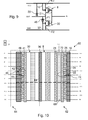
- the diodes 20 and 40 are here used to form an electrical protection device of the transistors 8 and 30 of the circuit 2.
- This device is configured to protect the transistors 8 and 30 against electrostatic discharges and to evacuate these electrostatic discharges to rails of circuit 2 power supply (not shown in the drawings).
- these supply rails are electrically connected to ground GND and to a source supplying the supply voltage VDD.
- the circuit 2 comprises a central protection including electrostatic discharges discharging occurring between the supply rails VDD and ground GND.
- the IN input of the circuit is brought to an electrical potential substantially equal to either GND ground or VDD voltage.
- the diodes 20 and 40 are therefore in a state that does not allow a passage of electric current.
- the electric potential of this input IN can be increased to a value higher than the voltage VDD.
- the diode 20 is in a state that passes an electric current. A local evacuation road is thus formed, before benefiting from the central protection.
- the central protection then allows the current to drain from VDD to GND.
- the diode 40 is in an on state. The electric current corresponding to the electrostatic discharge can thus be evacuated by the diodes 20 or 40 by short-circuiting the transistors 8 and 30.
- the electric potential of this output OUT can be lowered to a value lower than the voltage GND.
- the diode 40 is in a state that passes an electric current.
- the diode 20 is in an on state. A local evacuation road is thus formed, before benefiting from the central protection.
- the central protection then allows the current to be evacuated from the VDD rail to the GND rail.
- the electric current corresponding to the electrostatic discharge can thus be evacuated by the diodes 20 or 40 by short-circuiting the transistors 8 and 30.
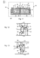
- the figure 10 represents an integrated circuit 60, able to replace the circuit 2 and comprising a protection device against electrostatic discharges.
- This circuit 60 comprises components 62 and 64.
- This circuit 60 is substantially identical to the circuit 2, except that the protection device is distinct from that of the circuit 2.
- the component 64 is here identical to the component 6.
- the zone 72 is formed by an extension of the box 14 in the vertical direction.
- This zone 72 has an n-type doping, so that the transistor 74 is a bipolar transistor PNP type.
- the diodes 20 and 40 and the transistor 74 are used here to form an electrical protection device of the transistors 8 and 30 of the circuit 60 distinct from that of the circuit 2.
- the use of the transistor 74 in this protection device makes it possible to improve the evacuation of electric current in case of electrostatic discharge.
- the transistor 74 has a gain in current, which makes it possible to obtain a faster discharge of the current.
- the transistor 74 also makes it possible to propose an additional path of local protection during negative overvoltages on the terminal IN relative to the voltage VDD (or positive overvoltage on VDD with respect to the terminal IN). Indeed, in the context of a conventional central protection, the overvoltage is clipped by the diode 40 and the supply protection, forcing the current to flow in the supply rails.
- Transistor 74 allows a direct local path between VDD and IN using the transistor's "snapback current" phenomenon. During a positive overvoltage on VDD, the junction between the zone 24 and 72 is in inverse, the leakage or ionization current by impact then makes it possible to increase locally the potential of the box 72 engaging the bipolar between VDD and IN.
- the transistor 74 When the diode 20 enters a conducting state, the transistor 74 in turn enters an on state, due to the current applied to its base. Thus, the discharge can be evacuated by greatly limiting the occurrence of overcurrent.
- the diode 20 When the diode 20 is reverse biased, the leakage current flowing through this diode 20 engages the transistor 74 causing the reversal current phenomenon, which allows to evacuate the discharge by greatly limiting the overcurrent.
- the figure 13 represents another example of the circuit 60.
- the diodes 20 and 40 and the transistor 74 are connected so as to protect the output OUT of the circuit 60 more specifically.
- This circuit is identical to that described in FIG. figure 12 , except that the electrodes E1 and F1 correspond, respectively, to the drains of transistors 8 and 30.
- the transistor 74 When the diode 20 enters a conducting state, the transistor 74 in turn enters an on state, due to the current applied to its base. Thus, the discharge can be evacuated by greatly limiting the occurrence of overcurrent.
- the diode 20 When the diode 20 is reverse biased, the leakage current flowing through this diode 20 engages the transistor 74, which in turn causes the reversal current phenomenon.
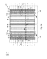
- the figure 14 represents an integrated circuit 80, able to replace the circuits 60 or 2 and comprising a protection device against electrostatic discharges.
- This circuit 80 comprises components 82 and 84.
- This circuit 80 is substantially identical to the circuit 60, except that the protection device is distinct from that of the circuit 60.
- the Figures 15 and 16 further represent these components 82 and 84.
- Component 82 is here identical to component 62.
- the circuit 80 further comprises a thyristor 96, formed by the zones 22, 66, the caissons 14 and 34 and the ground plane 86.
- the transistor 94 is of the NPN type.
- the diodes 20 and 40, the transistors 74 and 94 and the thyristor 96 are used here to form an electrical protection device of the transistors 8 and 30 of the circuit 80 which is distinct from that of the circuits 2 and 60.
- the use of the thyristor 96 in this protection device improves the evacuation of the electric current from an electrostatic discharge.
- the figure 18 represents another example of the protection device of the circuit 80, here connected so as to protect the output OUT of the circuit 80 more specifically.
- This circuit is identical to that described in FIG. figure 17 , except that the electrodes E1 and F1 correspond, respectively, to the drains of transistors 8 and 30.
- the diode 104 has a Zener breakdown voltage, in absolute value, greater than 2 volts and less than 20 volts, 15 volts or 10 volts.
- This breakdown voltage is adjustable during design and / or manufacturing steps of the circuit 100, in particular by adjusting the lateral dimension of the isolation trench 112 or the dopant concentration of the semiconductor zones forming the diode 104.
- the breakdown voltage of the diode 104 is essentially governed by the lateral dimension and no longer essentially by the dopant concentration.
- the component 102 comprises, in place of the transistor 8, a plurality of n-FET type MOS transistors identical to the transistor 8, this plurality including at least a first transistor 103. These transistors are electrically connected in cascode, forming a device 114. This device 114 extends electrically between an electrical GND of the circuit and a first electrode E1. This electrode E1 is here brought to a potential HV.
- the zone 110 has a dopant concentration of less than 10 17 cm -3 or less than 5 * 10 16 cm -3 .
- the diode 104 is used, in the event of the appearance of an electrostatic discharge, to trigger a protection device 116.
- Device 116 is configured to short-circuit device 114 and protect it against electrostatic discharges.
- the diode 104 In the presence of an electrostatic discharge on the electrode E1, this potential difference can increase substantially, to the point of exceeding the Zener breakdown voltage of the diode 104. In this case, the diode 104 enters a state allowing the circulation of current to the control electrode EC of the device 116, which protects the device 114.
- the control electrode of the device 116 can be either the trigger of a thyristor, the trigger of a triac, the base of a bipolar transistor, or the gate of a field effect transistor.
- the figure 23 illustrates an isolation trench 140 adapted to replace the trench 26.
- This trench 140 is similar to the trench 26, except that it has on its side walls a coating 142 of a second material electrically insulating.
- This second material is different from the electrically insulating material 144 forming the trench 26.
- This second coating is here a layer of silicon nitride Si 3 N 4 .
- the coating 142 has, for example, a thickness typically between 2 nm and 10 nm.
- the figure 24 is a component 150, able to replace the component 4.
- This component 150 is substantially identical to the component 4 except that it further comprises a deeply buried box 152.
- This box 152 is formed under the box 14 and in line with this caisson 14.
- This box 152 has an n-type doping.
- this box 152 has a dopant concentration of between 10 16 cm -3 and 10 18 cm -3 .
- the doping types of the transistors, ground planes, and respective wells of the components 4 and 6 can be inverted. The same is true for components 62 and 64, and for components 82 and 84.
- the component 6 can be omitted.
- the protection device is different from that described.
- the circuits 2, 60 and 80 may comprise a number of different transistors and / or of different nature from those described. These transistors may be connected to form a circuit different from the described CMOS logic inverter.
- the embodiments described for the zone 28 of the component 4 can be applied to the third zone of the component 6.
- the circuits 2, 60, 80, 100 and 120 comprise a deeply buried caisson.
- This deeply buried caisson for example presents an n-type doping for a p-type substrate 18, and is formed under and directly above the caissons 14 and 34. It is of course also possible to envisage a deep-buried p-type caisson for a n-type substrate 18.
- an epitaxial resumption can be performed on the zones 20, 22, 24, 42, 44, to avoid the difference in altitude with the transistors 8 and 30.
- the threshold voltage ranges of transistors 8 and 30 may be different.
- the gate lengths of transistors 8 and 30 may be different from 20 nm. These gate lengths may, for example, be greater than 20 nm, or less than 20 nm.
Landscapes
- Semiconductor Integrated Circuits (AREA)
- Metal-Oxide And Bipolar Metal-Oxide Semiconductor Integrated Circuits (AREA)
Applications Claiming Priority (1)
| Application Number | Priority Date | Filing Date | Title |
|---|---|---|---|
| FR1256800A FR2993402B1 (fr) | 2012-07-13 | 2012-07-13 | Circuit integre sur soi comprenant une diode laterale de protection contre des decharges electrostatiques |
Publications (1)
| Publication Number | Publication Date |
|---|---|
| EP2685497A1 true EP2685497A1 (de) | 2014-01-15 |
Family
ID=48700486
Family Applications (1)
| Application Number | Title | Priority Date | Filing Date |
|---|---|---|---|
| EP13175433.5A Withdrawn EP2685497A1 (de) | 2012-07-13 | 2013-07-05 | Integrierter SOI-Schaltkreis, der eine seitliche Diode zum Schutz gegen elektrostatische Entladungen umfasst |
Country Status (3)
| Country | Link |
|---|---|
| US (1) | US9653476B2 (de) |
| EP (1) | EP2685497A1 (de) |
| FR (1) | FR2993402B1 (de) |
Cited By (1)
| Publication number | Priority date | Publication date | Assignee | Title |
|---|---|---|---|---|
| CN111446245A (zh) * | 2019-01-17 | 2020-07-24 | 世界先进积体电路股份有限公司 | 半导体结构 |
Families Citing this family (2)
| Publication number | Priority date | Publication date | Assignee | Title |
|---|---|---|---|---|
| FR2996956B1 (fr) * | 2012-10-12 | 2016-12-09 | Commissariat Energie Atomique | Circuit integre comportant des transistors avec des tensions de seuil differentes |
| US9837439B1 (en) | 2016-08-12 | 2017-12-05 | Globalfoundries Inc. | Compensation of temperature effects in semiconductor device structures |
Citations (5)
| Publication number | Priority date | Publication date | Assignee | Title |
|---|---|---|---|---|
| US20020084490A1 (en) * | 2001-01-03 | 2002-07-04 | Ming-Dou Ker | ESD protection networks with NMOS-bound or PMOS-bound diode structures in a shallow-trench-isolation (STI) CMOS process |
| US20050269642A1 (en) * | 2004-06-03 | 2005-12-08 | Kabushiki Kaisha Toshiba | Semiconductor device |
| US20060284260A1 (en) * | 2005-06-21 | 2006-12-21 | Freescale Semiconductor, Inc. | Vertical diode formation in SOI application |
| US20070063284A1 (en) | 2005-08-01 | 2007-03-22 | Renesas Technology Corp. | Semiconductor device and semiconductor integrated circuit using the same |
| US20100200919A1 (en) * | 2009-02-06 | 2010-08-12 | Sony Corporation | Semiconductor device |
Family Cites Families (2)
| Publication number | Priority date | Publication date | Assignee | Title |
|---|---|---|---|---|
| US5923067A (en) * | 1997-04-04 | 1999-07-13 | International Business Machines Corporation | 3-D CMOS-on-SOI ESD structure and method |
| JP2001308330A (ja) * | 2000-04-19 | 2001-11-02 | Oki Electric Ind Co Ltd | 半導体集積回路装置 |
-
2012
- 2012-07-13 FR FR1256800A patent/FR2993402B1/fr active Active
-
2013
- 2013-07-02 US US13/933,441 patent/US9653476B2/en active Active
- 2013-07-05 EP EP13175433.5A patent/EP2685497A1/de not_active Withdrawn
Patent Citations (5)
| Publication number | Priority date | Publication date | Assignee | Title |
|---|---|---|---|---|
| US20020084490A1 (en) * | 2001-01-03 | 2002-07-04 | Ming-Dou Ker | ESD protection networks with NMOS-bound or PMOS-bound diode structures in a shallow-trench-isolation (STI) CMOS process |
| US20050269642A1 (en) * | 2004-06-03 | 2005-12-08 | Kabushiki Kaisha Toshiba | Semiconductor device |
| US20060284260A1 (en) * | 2005-06-21 | 2006-12-21 | Freescale Semiconductor, Inc. | Vertical diode formation in SOI application |
| US20070063284A1 (en) | 2005-08-01 | 2007-03-22 | Renesas Technology Corp. | Semiconductor device and semiconductor integrated circuit using the same |
| US20100200919A1 (en) * | 2009-02-06 | 2010-08-12 | Sony Corporation | Semiconductor device |
Non-Patent Citations (3)
| Title |
|---|
| "ESD Protection for SOI Technology using Under-the-BOX (substrate) Diode Structure", IEEE TRANSACTIONS ON DEVICE AND MATERIALS RELIABILITY, vol. 6, no. 2, June 2006 (2006-06-01) |
| AKRAM SALMAN ET AL: "ESD protection for SOI technology using an under-the-box (substrate) diode structure", ELECTRICAL OVERSTRESS/ELECTROSTATIC DISCHARGE SYMPOSIUM, 2004. EOS/ESD '04, IEEE, PISCATAWAY, NJ, USA, 19 September 2004 (2004-09-19), pages 1 - 7, XP031534189, ISBN: 978-1-58537-063-4 * |
| BENOIST T ET AL: "Improved ESD protection in advanced FDSOI by using hybrid SOI/bulk Co-integration", ELECTRICAL OVERSTRESS/ ELECTROSTATIC DISCHARGE SYMPOSIUM (EOS/ESD), 2010 32ND, IEEE, PISCATAWAY, NJ, USA, 3 October 2010 (2010-10-03), pages 1 - 6, XP031791641, ISBN: 978-1-58537-182-2 * |
Cited By (2)
| Publication number | Priority date | Publication date | Assignee | Title |
|---|---|---|---|---|
| CN111446245A (zh) * | 2019-01-17 | 2020-07-24 | 世界先进积体电路股份有限公司 | 半导体结构 |
| CN111446245B (zh) * | 2019-01-17 | 2022-09-23 | 世界先进积体电路股份有限公司 | 半导体结构 |
Also Published As
| Publication number | Publication date |
|---|---|
| FR2993402A1 (fr) | 2014-01-17 |
| US9653476B2 (en) | 2017-05-16 |
| US20140017858A1 (en) | 2014-01-16 |
| FR2993402B1 (fr) | 2018-02-02 |
Similar Documents
| Publication | Publication Date | Title |
|---|---|---|
| FR2993404A1 (fr) | Circuit integre sur soi comprenant un thyristor (scr) de protection contre des decharges electrostatiques | |
| FR3005203A1 (fr) | Circuit integre sur soi comprenant un transistor de protection contre des decharges electrostatiques | |
| FR2812972A1 (fr) | Dispositif a semiconducteur consistant en un thyristor pour la protection contre les decharges electrostatiques | |
| FR2953995A1 (fr) | Interrupteur de puissance bidirectionnel commandable a la fermeture et a l'ouverture | |
| EP2685501A1 (de) | Integrierter SOI-Schaltkreis, der einen darunterliegenden Schutztransistor umfasst | |
| EP2685499A1 (de) | Integrierter SOI-Schaltkreis, der einen Triac zum Schutz gegen elektrostatische Entladungen umfasst | |
| FR2982416A1 (fr) | Dispositif electronique de protection contre les decharges electrostatiques | |
| EP2573808A1 (de) | Integrierter Schaltkreis mit FD-SOI-Technologie mit Gehäuseunterteilung und Mitteln zur Polarisierung der entgegengesetzten Dotierungsmassenpläne, die in einem und demselben Gehäuse vorhanden sind | |
| EP0581625B1 (de) | Multifunktionale elektronische Vorrichtung, insbesondere Element mit dynamischem, negativem Widerstandsverhalten und Zugehöriges Herstellungsverfahren | |
| EP2835825A1 (de) | Integrierter SOI-Schaltkreis, der mit einer Schutzvorrichtung gegen elektrostatische Entladungen ausgestattet ist | |
| FR2993401A1 (fr) | Transistor mos sur soi protege contre des surtensions | |
| EP2685502A1 (de) | Integrierter SOI-Schaltkreis, der einen bipolaren Transistor mit Isolationsrinnen unterschiedlicher Tiefe umfasst | |
| FR3001085A1 (fr) | Dispositif semiconducteur bidirectionnel de protection contre les decharges electrostatiques, utilisable sans circuit de declenchement | |
| EP2685504A1 (de) | Tunneleffekttransistor | |
| EP2775529A2 (de) | Transistor mit Tunneleffekt | |
| EP2685497A1 (de) | Integrierter SOI-Schaltkreis, der eine seitliche Diode zum Schutz gegen elektrostatische Entladungen umfasst | |
| FR3057394A1 (fr) | Dispositif de protection contre les decharges electrostatiques avec circuit de declenchement distribue | |
| EP0921571B1 (de) | ESD-Schutzbauteil | |
| WO2000025363A1 (fr) | Composant de puissance portant des interconnexions | |
| WO2014057112A1 (fr) | Circuit integre comportant des transistors avec des tensions de seuil differentes | |
| EP4297090A1 (de) | Mikroelektronische anordnung mit zwei feldeffekttransistoren | |
| EP0697734B1 (de) | Schutzschaltung gegen elektrostatische Entladung | |
| EP4287263A1 (de) | Lateraler bipolartransistor | |
| EP0996165A1 (de) | Leistungsbauelement mit Verbindungen | |
| FR2995139A1 (fr) | Transistor mos |
Legal Events
| Date | Code | Title | Description |
|---|---|---|---|
| PUAI | Public reference made under article 153(3) epc to a published international application that has entered the european phase |
Free format text: ORIGINAL CODE: 0009012 |
|
| AK | Designated contracting states |
Kind code of ref document: A1 Designated state(s): AL AT BE BG CH CY CZ DE DK EE ES FI FR GB GR HR HU IE IS IT LI LT LU LV MC MK MT NL NO PL PT RO RS SE SI SK SM TR |
|
| AX | Request for extension of the european patent |
Extension state: BA ME |
|
| 17P | Request for examination filed |
Effective date: 20140711 |
|
| RBV | Designated contracting states (corrected) |
Designated state(s): AL AT BE BG CH CY CZ DE DK EE ES FI FR GB GR HR HU IE IS IT LI LT LU LV MC MK MT NL NO PL PT RO RS SE SI SK SM TR |
|
| STAA | Information on the status of an ep patent application or granted ep patent |
Free format text: STATUS: THE APPLICATION IS DEEMED TO BE WITHDRAWN |
|
| 18D | Application deemed to be withdrawn |
Effective date: 20160202 |