EP2685507B1 - Module solaire doté d'agencements de raccordement pour raccord électrique extérieur - Google Patents
Module solaire doté d'agencements de raccordement pour raccord électrique extérieur Download PDFInfo
- Publication number
- EP2685507B1 EP2685507B1 EP12175486.5A EP12175486A EP2685507B1 EP 2685507 B1 EP2685507 B1 EP 2685507B1 EP 12175486 A EP12175486 A EP 12175486A EP 2685507 B1 EP2685507 B1 EP 2685507B1
- Authority
- EP
- European Patent Office
- Prior art keywords
- connection
- substrate
- solar module
- module
- housing
- Prior art date
- Legal status (The legal status is an assumption and is not a legal conclusion. Google has not performed a legal analysis and makes no representation as to the accuracy of the status listed.)
- Active
Links
Images


Classifications
-
- H—ELECTRICITY
- H10—SEMICONDUCTOR DEVICES; ELECTRIC SOLID-STATE DEVICES NOT OTHERWISE PROVIDED FOR
- H10F—INORGANIC SEMICONDUCTOR DEVICES SENSITIVE TO INFRARED RADIATION, LIGHT, ELECTROMAGNETIC RADIATION OF SHORTER WAVELENGTH OR CORPUSCULAR RADIATION
- H10F77/00—Constructional details of devices covered by this subclass
- H10F77/93—Interconnections
- H10F77/933—Interconnections for devices having potential barriers
- H10F77/935—Interconnections for devices having potential barriers for photovoltaic devices or modules
-
- H—ELECTRICITY
- H02—GENERATION; CONVERSION OR DISTRIBUTION OF ELECTRIC POWER
- H02S—GENERATION OF ELECTRIC POWER BY CONVERSION OF INFRARED RADIATION, VISIBLE LIGHT OR ULTRAVIOLET LIGHT, e.g. USING PHOTOVOLTAIC [PV] MODULES
- H02S40/00—Components or accessories in combination with PV modules, not provided for in groups H02S10/00 - H02S30/00
- H02S40/30—Electrical components
- H02S40/34—Electrical components comprising specially adapted electrical connection means to be structurally associated with the PV module, e.g. junction boxes
-
- H—ELECTRICITY
- H10—SEMICONDUCTOR DEVICES; ELECTRIC SOLID-STATE DEVICES NOT OTHERWISE PROVIDED FOR
- H10F—INORGANIC SEMICONDUCTOR DEVICES SENSITIVE TO INFRARED RADIATION, LIGHT, ELECTROMAGNETIC RADIATION OF SHORTER WAVELENGTH OR CORPUSCULAR RADIATION
- H10F19/00—Integrated devices, or assemblies of multiple devices, comprising at least one photovoltaic cell covered by group H10F10/00, e.g. photovoltaic modules
- H10F19/30—Integrated devices, or assemblies of multiple devices, comprising at least one photovoltaic cell covered by group H10F10/00, e.g. photovoltaic modules comprising thin-film photovoltaic cells
- H10F19/31—Integrated devices, or assemblies of multiple devices, comprising at least one photovoltaic cell covered by group H10F10/00, e.g. photovoltaic modules comprising thin-film photovoltaic cells having multiple laterally adjacent thin-film photovoltaic cells deposited on the same substrate
-
- H—ELECTRICITY
- H10—SEMICONDUCTOR DEVICES; ELECTRIC SOLID-STATE DEVICES NOT OTHERWISE PROVIDED FOR
- H10F—INORGANIC SEMICONDUCTOR DEVICES SENSITIVE TO INFRARED RADIATION, LIGHT, ELECTROMAGNETIC RADIATION OF SHORTER WAVELENGTH OR CORPUSCULAR RADIATION
- H10F19/00—Integrated devices, or assemblies of multiple devices, comprising at least one photovoltaic cell covered by group H10F10/00, e.g. photovoltaic modules
- H10F19/80—Encapsulations or containers for integrated devices, or assemblies of multiple devices, having photovoltaic cells
-
- Y—GENERAL TAGGING OF NEW TECHNOLOGICAL DEVELOPMENTS; GENERAL TAGGING OF CROSS-SECTIONAL TECHNOLOGIES SPANNING OVER SEVERAL SECTIONS OF THE IPC; TECHNICAL SUBJECTS COVERED BY FORMER USPC CROSS-REFERENCE ART COLLECTIONS [XRACs] AND DIGESTS
- Y02—TECHNOLOGIES OR APPLICATIONS FOR MITIGATION OR ADAPTATION AGAINST CLIMATE CHANGE
- Y02E—REDUCTION OF GREENHOUSE GAS [GHG] EMISSIONS, RELATED TO ENERGY GENERATION, TRANSMISSION OR DISTRIBUTION
- Y02E10/00—Energy generation through renewable energy sources
- Y02E10/50—Photovoltaic [PV] energy
Definitions
- Photovoltaic layer systems for the conversion of sunlight into electrical energy are well known. Commonly, these are referred to as “solar cells", wherein the term “thin film solar cells” refers to layer systems with thicknesses of only a few micrometers, which require a carrier substrate for sufficient mechanical strength. Since only voltage levels of less than 1 volt are usually achieved with individual solar cells, it is customary to connect a plurality of solar cells in a solar module in series. Thin-film solar modules offer the particular advantage that the solar cells can already be connected in integrated form during layer production. Thin-film solar modules are usually formed in a composite disk structure in which the solar cells are located between two individual disks firmly connected. Thin-layer solar modules have already been described many times in the patent literature.
- connection housings which form a basis for electrical connection components such as connection conductors or connection plugs and enable an external electrical connection.
- connection housing is known for example from German patent application no. 102005025632 A1 known.
- the international patent application WO 2012/055808 A2 discloses an alternative approach in which the collecting electrode or bus bar is electrically connected to a foil conductor which is led out of the composite between the two substrates.
- the object of the present invention is to develop conventional solar modules so that an automated production is even easier and cheaper to carry out.
- a solar module in particular a thin-film solar module
- the two substrates are formed such that at least one substrate edge of one substrate is recessed inward relative to an opposite substrate edge of the other substrate, such that a module edge zone is formed with a protruding substrate edge region (of the other substrate).
- the modulus edge zone is formed only on one module side (or module edge) of the generally rectangular or parallelepiped-shaped solar module, it being equally conceivable for such a module edge zone to be located on mutually opposite or adjoining module sides (or modules). Module edges), so that the solar module two or more module edge zones having.
- the two substrates can contain, for example, inorganic glass, polymers or metal alloys and can be designed as rigid plates or flexible films depending on layer thickness and material properties.
- the solar module is preferably a thin-film solar module with thin-film solar cells connected in series in integrated form.
- the semiconductor layer consists of a chalcopyrite compound, which is in particular an I-III-VI semiconductor from the group copper-indium / gallium-disulphide / diselenide (Cu (In / Ga) (S / SE) 2 )
- Cu (In / Ga) (S / SE) 2 copper-indium diselenide
- CuInSe 2 or CIS copper indium diselenide
- the solar module comprises two connection arrangements, which are each assigned to a collecting electrode.
- the connection arrangements each have a connection strip which is electrically conductively connected to the associated collecting electrode and a connection housing fastened to the composite with a connection component which is electrically conductively connected to the connection strip, for example a connecting line or a connection plug which serves for an external electrical connection.
- the two connection arrangements can be common connection housing or each have a separate connection housing.
- the terminal strips each comprise a foil conductor, which consists for example of a metal such as aluminum or tin-plated copper, but other electrically conductive materials can also be used which can be processed into foils. Examples of these are aluminum, gold, silver or tin and alloys thereof.
- the film conductor may have, for example, a thickness in the range of 0.03 mm to 0.3 mm, a length in the range of 30 to 50 mm and a width in the range of 5 to 15 mm.
- a connection between collecting electrode and connecting band takes place, for example, by welding, bonding, soldering, clamping, bonding by means of an electrically conductive adhesive or ultrasonic bonding.
- the connecting strips are each electrically connected by an electrical bus conductor with the associated collecting electrode, which allows a simple and cost-effective contacting at a convenient location, for example, adjacent to the module edge.
- the bus bar is preferably in the form of a ribbon or strip and printed, for example, in the (screen) printing method on the electrode area forming the collecting electrode.
- the bus bar it is also conceivable to design the bus bar as a foil conductor.
- a connection between the bus bar and the connection strip is effected, for example, by welding, bonding, soldering, clamping, bonding by means of an electrically conductive adhesive or ultrasonic bonding.
- connection band between the two substrates is laterally out of the composite led out, wherein the connecting band is guided around the inwardly recessed substrate edge around on the substrate outer surface, which allows easy production and contacting by the connection component in the connection housing. Due to the protruding edge of the substrate, the connection tape is protected against mechanical forces.
- the terminal housing is made, for example, of an electrically insulating material, which offers thermoplastic materials and elastomers for industrial production, which can be processed by injection molding.
- thermoplastics and elastomers for example, polyamide, polyoxymethylene, polybutylene terephthalate or ethylene-propylene-diene rubber is used.
- potting materials such as acrylate or epoxy resin systems can be used.
- connection housing from metal or another electrically conductive material with electrically insulating inserts.
- the connection housing can accommodate further functional elements such as diodes or a control electrics.
- connection housing on the composite is advantageously carried out by gluing, which can be hermetically sealed by the bonding, the interior of the connection housing against gases, water or moisture.
- the electrical contact points are protected against corrosion.
- an adhesive strand or an adhesive tape with an acrylic, polyurethane or polyisobutylene-based adhesive can be used for bonding.
- the adhesive is applied to a bottom surface of the terminal housing and / or on the composite and the connection housing mounted on the composite.
- the connection housing is arranged at least in sections in the module edge zone, whereby a protection of the laterally led out of the composite connection band from external influences can be achieved in a simple manner.
- connection housing has a sealing compound chamber with a cavity which serves to receive a connection band section guided around the substrate edge.
- a sealing compound is introduced, which abuts the around the substrate edge guided around the connecting band section and seals to the outside.
- the sealing compound chamber has a wall section delimiting the cavity, which is formed tapering towards the protruding substrate edge region.
- the tapered wall section allows the sealing compound, for example in the form of a sealing compound bead or sealing compound strand, to be applied to the projecting substrate edge region, in particular selectively onto the connecting band section guided around the substrate edge, and then the connection housing can be placed on the composite.
- the tapered wall portion not only a shearing of the sealant can be avoided by the around the substrate edge around the connecting band portion, but the sealing compound is also pressed to the connecting band section, so that a gas- and watertight sealing of the guided around the edge of the substrate connecting band is ensured. It is thus not necessary for the sealant to be introduced into the sealant chamber before the connection housing is fastened becomes.
- the solar module thus enables in a particularly advantageous manner, an automated cost-effective production in industrial series production with a reliable gas and waterproof sealing of the connection tape.
- the wall section of the sealing mass chamber tapering towards the protruding substrate edge region can be formed in a simple manner by virtue of the fact that the wall section has a chamfered bottom surface fitting in sections over the projecting substrate edge region.
- This also allows sealing compound to be located between the beveled bottom surface and the protruding substrate edge region, whereby an adhesive attachment of the connection housing to the projecting substrate edge region can advantageously be achieved when using an adhesive sealant.
- the sticking of the connection housing to the composite can thus be carried out fully automatically in a simple manner.
- the terminal housing is glued to the back of the module.
- connection tape is provided with an adhesive, for example a double-sided adhesive tape, which allows a simple and cost-effective attachment of the connection tape to the substrate, as well as its positional fixation.
- connection band has a tinned end portion for connection to the connection component. This allows a simple electrical connection between connecting band and connecting component.
- connection housing has a removable insert part inserted into a housing opening, wherein access to a contact chamber for connecting the connection strip to the connection component is created by the housing opening.
- the thin-film solar module 1 comprises a plurality of thin-film solar cells 2 connected in series with each other in integrated form, of which in Fig. 1 two are shown by way of example. It is understood that in thin-film solar modules typically more than 100 thin film solar cells 2 are connected in series with each other.
- the thin-film solar module 1 is formed in a composite disk structure and comprises a back-side carrier substrate 7 and a front-side cover substrate 16, each made of an electrically insulating material, such as glass or plastic, equally other electrically insulating materials with sufficient strength and inert behavior compared to the process steps performed can be used.
- the substrates 7, 16 can be designed as rigid plates or flexible films.
- the backside support substrate 7 is a rigid low-transmittance glass plate
- the front-side cover substrate 16 is a rigid glass plate of tempered extra-white low-iron glass which is transparent to sunlight, so that the thin-film solar cells 2 are on the front side (Side I) of the cover substrate 16 incident light can be irradiated.
- the cover substrate 16 serves to seal and mechanically protect the thin film solar cells 2.
- the layer structure 6 comprises a back electrode layer 9, for example of an opaque metal such as molybdenum, which is applied to the carrier substrate 7 by sputtering.
- the back electrode layer 9 has, for example, a layer thickness of about 1 ⁇ m.
- the back electrode layer 9 can equally consist of a layer stack with different individual layers.
- the layer structure 6 comprises an absorber layer 8 applied to the back electrode layer 9, which in turn is composed of several layers.
- the absorber layer 8 comprises a p-doped semiconductor layer 10, for example of a p-type chalcopyrite semiconductor.
- the semiconductor layer 10 has, for example, a layer thickness of 500 nm to 5 ⁇ m, which is in particular approximately 2 ⁇ m.
- a buffer layer 11 is deposited, which consists for example of cadmium sulfide (CdS) and intrinsic zinc oxide (i-ZnO).
- a front electrode layer 12 is applied, for example, by vapor deposition.
- the front electrode layer 12 is transparent to radiation in a spectral region that is sensitive to the semiconductor layer 10 ("window layer") and is based, for example, on a doped metal oxide, in particular n-conducting, aluminum-doped zinc oxide.
- the layer thickness of the front electrode layer 12 is for example 300 nm.
- the layer structure 6 is in a plurality of photovoltaically active regions divided. The subdivision is carried out by incisions 13, which were introduced by a suitable structuring technology such as laser writing and mechanical ablation in the layer structure 6.
- adjacent thin-film solar cells 2 are each connected in series with each other via a first electrode region 14 of the back electrode layer 9, collecting electrodes 5 of opposing polarity of the thin-film solar cells interconnected by the two marginal second electrode regions 14 'of the back electrode layer 9 being formed.
- the total voltage generated by the serially connected thin-film solar cells 2 which results as the sum of the cell voltages generated by the individual thin-film solar cells 2, can be tapped.
- the two collecting electrodes 5 are each electrically connected to a band-shaped bus bar 17, which in Fig. 2 is shown.
- the bus bars 17 are printed on the associated second electrode area 14 ', for example by screen printing.
- the bus bars 17 advantageously allow contacting at a suitable location, for example in the vicinity of a module edge 19.
- thermoplastic intermediate layer 15 which consists for example of polyvinyl butyral (PVB) or ethylene vinyl acetate (EVA).
- PVB polyvinyl butyral
- EVA ethylene vinyl acetate
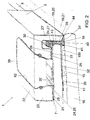
- connection arrangement 100 which contains a connection housing 3 for an external electrical connection of a resulting collecting electrode 5
- Fig. 2 shows a perspective view of the terminal assembly 100 with a sectional view of the terminal housing 3, wherein the cutting line along a shorter transverse direction of the cuboid or rectangular thin-film solar module 1 is guided.
- Fig. 3A the connection housing 3 with connection cable 4 is shown in a perspective view.
- Fig. 3B shows the connection housing 3 in a sectional view, wherein the cutting line is guided in the longitudinal direction or perpendicular to the transverse direction of the thin-film solar module 1.
- a carrier substrate edge 20 of the carrier substrate 7 is set back inwards (transversely) relative to an opposite cover substrate edge 21 of the cover substrate 16, so that there is a (spatial) module edge zone 18 with a projecting substrate edge region 40 results.
- the width of the projecting substrate edge region 40 along the shorter transverse direction of the thin-film solar module 1 is approximately 2 to 3 mm.
- module edge zone 18 is here and further understood the space zone, which is bounded by the module edge 19 and an aligned extension of the protruding deck substrate 21 and an aligned extension of the outer surface (side IV) of the support substrate 7.
- the module edge 19 results from the carrier substrate edge 20 and the cover substrate edge 21, and by a lateral edge surface 41 of the layer structure 6 and the intermediate layer 15th
- the thin-film solar module 1 has two identically constructed connection arrangements 100, each of which comprises a connection housing 3 arranged at the rear. Each terminal assembly 100 is associated with a collecting electrode 5. In Fig. 2 For simplicity of illustration, only one terminal assembly 100 is shown. Through the two terminal housing 3, the thin-film solar module 1 can be connected to other thin-film solar modules to form a module string or connected to an electrical load, such as an inverter. Each terminal housing 3 has for this purpose via a connection cable 4, wherein a plug component can be provided equally.
- the connection housing 3 is made, for example, as a cuboid injection molded part made of plastic and has for example a length of 50 mm, a width of 20 mm and a height of 10 mm.
- the connection housing 3 can be at least mentally divided into different housing sections. It comprises a base section 22 and side wall sections 23, 23 'which, together with the thin-film solar module 1, surround a cavity 24.
- the cavity 24 is divided by a support strut 25 into a contact chamber 26 and a sealant chamber 27, the function of which will be explained below.
- the terminal housing 3 sits on one of three first side wall portions 23 and the support strut 25 formed bottom surface 31 of the outer surface (side IV) of the support substrate 7 and is fixedly connected by an adhesive layer 28 to the support substrate 7.
- the adhesive layer 28 is made for example, from an acrylate or polyurethane adhesive. In addition to a simple and durable connection, these adhesives fulfill a sealing function against water and air and protect the electrical components contained in the connection housing 3 from corrosion.
- a parallel to the module edge 19 extending second side wall portion 23 'of the terminal housing 3 has a beveled bottom surface 31', which is seated with a contact edge 44 of the inner surface (side II) of the cover substrate 16 in the projecting substrate edge region 40.
- sealant 29 is also between the bottom surface 31 'and the protruding substrate edge region 40, so that in an adhesive sealant attachment of the terminal housing 3 on the composite and excellent sealing of the sealing chamber 27 is achieved to the outside.
- the sealing compound 29 penetration of water and air into the connection housing 3 in the region of the second side wall section 23 'can be reliably and reliably prevented.
- a sealing compound 29 made of polyisobutylene can be used for this purpose.
- connection housing 3 in which the seal mass chamber 27 limiting second side wall portion 23 'of the terminal housing 3 tapers to the contact edge 44, ie tapered.
- the bus bar 17 electrically connected to the associated collecting electrode 5 and the connecting cable 4 are electrically connected to one another by a connection strip 32.
- the connecting band 32 is in Fig. 4A shown in the uninstalled state. It comprises a foil conductor 33 made of a metallic material, for example aluminum or copper, on which on one side a double-sided adhesive tape 34 with an adhesive based on acrylic, polyurethane or polyisobutylene is applied.
- the connecting band 32 has two adhesive tape-free end portions 35, 35 ', wherein an end portion 35' is provided with a tin layer 36.
- the connecting band 32 has a length in the range of 30 to 50 mm and a width of about 10 mm.
- the connecting band 32 is laid around the inwardly recessed carrier sub-strand 20 in the installed state, wherein the non-tinned end portion 35 on the inside of the carrier substrate 7 is electrically connected to the bus bar 17 and the tinned end portion 35 'on the outer surface (page IV). of the carrier substrate 7 comes to rest.
- the adhesive tape 34 By means of the adhesive tape 34, the connecting band 32 is fastened to the carrier substrate 7 and fixed in its position. A permanent electrical connection between the non-tinned end portion 35 and the bus bar 17, for example, by Ultraschallverlötung.
- a connection band section 43 guided around the carrier substrate edge 20 is sealed in a water-tight and airtight manner by the (adjacent) sealing compound 29 toward the outside environment.
- the sealing compound 29 is applied in a targeted manner to the connecting band section 43 before the connecting housing 3 is put on.
- the bevelled bottom surface 31 'or the projecting substrate edge region 40 towards the tapered second side wall portion 23' a shearing of the sealant 29 can be avoided by the connecting band portion 43.
- the sealant 29 is pressed to the connecting band portion 43, whereby the seal is improved. This is especially true for the in Fig. 3C shown variant.
- the terminal housing 3 On the outside of the carrier substrate 7, the terminal housing 3 is placed so that the tinned end portion 35 'is located within the contact chamber 26. As in the sectional view of Fig. 3B can be seen, an exposed end portion 38 of an inner cable conductor 37 of the connecting cable 4 to the tinned end portion 35 'is electrically connected, for example by a solder joint, which in Fig. 3B not shown in detail.
- the terminal housing 3 has for this purpose a inserted into a housing opening 42, removable insert 39, wherein through the housing opening 42 a free access to the contact chamber 26 for connecting end portion 38 and end portion 35 'is provided after fixing the terminal housing 3 on thin-film solar module 1.
- connection arrangements 100 for the voltage connections 5 can be produced fully automatically in a simple and cost-effective manner.
- the connecting strips 32 are fastened on the inside (side III) of the carrier substrate 7 and guided around the carrier substrate edge 20 to the outside of the carrier substrate 7.
- the end portions 35 of the connecting bands 32 are firmly connected to the respectively associated bus bar 17, for example by ultrasonic welding.
- the sealing compound 29 has been applied to the protruding substrate edge region 40, in particular to the two connecting strip sections 43
- the two connection housings 3 are placed on the outside of the carrier substrate 7 and respectively through the adhesive layer 28 attached.
- the two connection arrangements 100 can be arranged on only one module edge 19 or, for example, also distributed on two opposite module edges 19, which each have a module edge zone 18. Equally, it would also be possible that only a single connection housing 3 is provided for an external electrical connection of the two collecting electrodes 5. In this case, care should be taken that an electrical flashover between the two connection strips 32 is avoided, which can be achieved for example by an insulating partition.
Landscapes
- Photovoltaic Devices (AREA)
Claims (10)
- Module solaire (1), en particulier module solaire à couches minces, comprenant:un composite stratifié composé de deux substrats (7, 16), où au moins un bord de substrat (20) de l'un des substrats (7) est déplacé vers l'intérieur par rapport à un bord de substrat opposé (21) de l'autre substrat (16), de telle manière qu'une zone de bord d'un module (18) est formée avec une zone en saillie de bord du substrat (40),un circuit en série composé d'une pluralité de cellules solaires (2) situé entre les deux substrats (7, 16), qui dispose de deux électrodes collectives (5) pour saisir une tension totale générée par les cellules solaires (2),deux configurations de connexion (100), dont chacune est assignée à une électrode collective (5), où chaque arrangement de connexion (100) présente:- une bande de raccordement (32) reliée électriquement à l'électrode collective assignée (5) qui est guidée dans la zone de bord du module (18) entre les deux substrats (7, 16) autour du bord du substrat décalé vers intérieur (20) sur une surface extérieure du substrat,- un boîtier de connexion (3) attaché au composite avec un composant de connexion (4) relié électriquement à la bande de raccordement (32), où le boîtier de connexion (3) présente une chambre pour une masse d'étanchéité (27) qui contient une masse d'étanchéité (29) qui scelle la bande de raccordement (32) dans une section de bande de raccordement (43) guidée autour du bord du substrat (20), où une section de paroi (23') du boîtier de connexion (3) limitant la chambre de la masse d'étanchéité (27) est formée de façon pointue vers la zone en saillie de bord du substrat (40).
- Module solaire (1) selon la revendication 1, où la section de paroi (27') limitant la chambre de la masse d'étanchéité (27)) du boîtier de raccordement (3) présente une surface inférieure (31') chanfreinée et adjacente par sections à la zone en saillie du bord de substrat (40).
- Module solaire (1) selon la revendication 2, où le boîtier de connexion (3) est fixé par une masse d'étanchéité (29) entre la surface inférieure (31') chanfreinée et la zone en saillie du substrat (40).
- Module solaire (1) selon l'une des revendications 1 à 3, où le ruban de connexion (32) de l'arrangement de connexion (100) respectif est pourvu d'un adhésif (34), par exemple un ruban adhésif à double face, pour la fixation sur un substrat (7).
- Module solaire (1) selon l'une des revendications 1 à 8, où la bande de raccordement (32) de l'arrangement de connexion (100) respectif est reliée électriquement à l'électrode collective associée (5) par un conducteur collectif en forme de bande (17).
- Module solaire (1) selon la revendication 5, où la bande de raccordement (32) est solidement rattachée au conducteur collectif (17), par exemple par une connexion par ultrasons.
- Module solaire (1) selon l'une des revendications 1 à 6, où la bande de connexion (32) de l'arrangement de connexion (100) respectif dispose d'une section d'extrémité étamée (35') pour la connexion au composant de connexion (4).
- Module solaire (1) selon l'une des revendications 1 à 7, où le boitier de connexion (3) de l'arrangement de connexion (100) respectif présente une pièce d'insertion (39) amovible insérée dans une ouverture du boitier (42) (39), où l'accès à une chambre de contact (26) pour la connexion électrique de la bande de raccordement (32) et le composant de connexion (4) est obtenu par l'ouverture du boitier.
- Module solaire (1) selon l'une des revendications 1 à 8, où les deux arrangements de connexion (100) disposent d'un boitier de connexion commun (3).
- Procédé pour la production d'un module solaire, en particulier un module solaire à couches minces (1), avec les étapes suivantes:- formation d un circuit en série à partir d'une pluralité de cellules solaires (2) sur un premier substrat (7), où le circuit en série dispose de deux électrodes collectives (5) pour saisir la tension totale générée par les cellules solaires (2) ;- connexion électrique des électrodes de collecte (5) avec des bandes de raccordement (32) ;- fabrication d'un composite à partir du premier substrat (7) avec un deuxième substrat (16), où au moins un bord de substrat (20) de l'un des substrats (7) par rapport à un bord de substrat (21) opposé de l'autre substrat (16) est déplacé vers l'intérieur, de sorte qu'une zone de bord du module (18) est formée avec une zone de substrat en saillie (40), où les bandes de raccordement (32) dans la zone de bord du module (18) entre les deux substrats (7, 16) autour du bord de substrat décalé vers l'intérieur (20) est guidé sur une surface extérieure du substrat (20); de sorte qu'un substrat (20) est déplacé vers l'intérieur ;- l'application d'une masse d'étanchéité (29) sur l'autre substrat (l6) au moins sur une section de bande de raccordement (43) autour du substrat (20);- pose d'un boîtier de connexion (3) avec un ou plusieurs composants de connexion (4) pour une connexion électrique externe au composite, où le boitier de connexion présente une chambre pour une masse d'étanchéité (27) pour recevoir la masse d'étanchéité (29) avec une section de paroi (23') de forme pointue qui est montée sur la zone du substrat (40) en saillie;- connexion électrique des bandes de raccordement (32) reliée aux électrodes collectives (5) avec les composants de connexion (4).
Priority Applications (2)
| Application Number | Priority Date | Filing Date | Title |
|---|---|---|---|
| ES12175486T ES2772201T3 (es) | 2012-07-09 | 2012-07-09 | Módulo solar con conjuntos de conexión para conexión eléctrica externa |
| EP12175486.5A EP2685507B1 (fr) | 2012-07-09 | 2012-07-09 | Module solaire doté d'agencements de raccordement pour raccord électrique extérieur |
Applications Claiming Priority (1)
| Application Number | Priority Date | Filing Date | Title |
|---|---|---|---|
| EP12175486.5A EP2685507B1 (fr) | 2012-07-09 | 2012-07-09 | Module solaire doté d'agencements de raccordement pour raccord électrique extérieur |
Publications (2)
| Publication Number | Publication Date |
|---|---|
| EP2685507A1 EP2685507A1 (fr) | 2014-01-15 |
| EP2685507B1 true EP2685507B1 (fr) | 2019-11-13 |
Family
ID=46507904
Family Applications (1)
| Application Number | Title | Priority Date | Filing Date |
|---|---|---|---|
| EP12175486.5A Active EP2685507B1 (fr) | 2012-07-09 | 2012-07-09 | Module solaire doté d'agencements de raccordement pour raccord électrique extérieur |
Country Status (2)
| Country | Link |
|---|---|
| EP (1) | EP2685507B1 (fr) |
| ES (1) | ES2772201T3 (fr) |
Family Cites Families (7)
| Publication number | Priority date | Publication date | Assignee | Title |
|---|---|---|---|---|
| DE4324318C1 (de) | 1993-07-20 | 1995-01-12 | Siemens Ag | Verfahren zur Serienverschaltung einer integrierten Dünnfilmsolarzellenanordnung |
| US7534956B2 (en) * | 2003-04-10 | 2009-05-19 | Canon Kabushiki Kaisha | Solar cell module having an electric device |
| DE102005025632B4 (de) | 2005-06-03 | 2015-09-17 | Te Connectivity Germany Gmbh | Verbindungsvorrichtung für den Anschluss elektrischer Folienleiter |
| WO2008148524A2 (fr) * | 2007-06-04 | 2008-12-11 | Tyco Electronics Amp Gmbh | Module solaire avec un élément de connecteur électrique |
| EP2165122A1 (fr) * | 2007-06-08 | 2010-03-24 | Robert Stancel | Ensemble de branchement électrique pour montage en bordure |
| EP2200097A1 (fr) | 2008-12-16 | 2010-06-23 | Saint-Gobain Glass France S.A. | Procédé pour la fabrication d'un dispositif photovoltaïque et système de formation d'un objet |
| WO2012055808A2 (fr) | 2010-10-25 | 2012-05-03 | Saint-Gobain Glass France | Module solaire équipé d'un élément de raccordement |
-
2012
- 2012-07-09 EP EP12175486.5A patent/EP2685507B1/fr active Active
- 2012-07-09 ES ES12175486T patent/ES2772201T3/es active Active
Non-Patent Citations (1)
| Title |
|---|
| None * |
Also Published As
| Publication number | Publication date |
|---|---|
| ES2772201T3 (es) | 2020-07-07 |
| EP2685507A1 (fr) | 2014-01-15 |
Similar Documents
| Publication | Publication Date | Title |
|---|---|---|
| EP2758993B1 (fr) | Module solaire à couches minces à câblage en série et procédé de câblage en série de cellules solaires à couches minces | |
| WO2012055808A2 (fr) | Module solaire équipé d'un élément de raccordement | |
| EP2855180A1 (fr) | Vitre de toit avec module photovoltaïque intégré | |
| EP2855146A1 (fr) | Panneau de toit pourvu d'un module photovoltaïque intégré | |
| DE102009026149A1 (de) | Verbundsystem für Photovoltaik-Module | |
| WO2013143821A1 (fr) | Module photovoltaïque doté d'un dispositif refroidisseur | |
| EP2761673B1 (fr) | Module solaire doté d'une boîte de raccordement ainsi que son procédé de fabrication | |
| DE102007052971A1 (de) | Kontaktierung und Modulverschaltung von Dünnschichtsolarzellen auf polymeren Trägern | |
| DE112011102882T5 (de) | Flexible gebäudeintegrierte Photovoltaikstruktur | |
| DE112008001045T5 (de) | Solarzellenmodul | |
| EP1886357B1 (fr) | Procede de guidage de bandes de contact dans des modules solaires et module solaire | |
| EP2352171A1 (fr) | Arrangement des cellules solaires, panneau solaire en couche mince et méthode de fabrication | |
| EP2929570A1 (fr) | Module solaire avec boîte de jonction | |
| EP2685507B1 (fr) | Module solaire doté d'agencements de raccordement pour raccord électrique extérieur | |
| EP2769418A1 (fr) | Module solaire à conducteur en ruban plat ainsi que son procédé de fabrication | |
| DE102022128223B4 (de) | Solarzellenmodul und Verfahren zur Herstellung eines Solarzellenmoduls | |
| DE102010013850A1 (de) | Verfahren zum elektrischen Verbinden von Solarzellen für ein Solarmodul | |
| DE102019122213A1 (de) | Verfahren zur elektrisch leitenden Kontaktierung eines mindestens eine Schutzschicht aufweisenden optoelektronischen Bauelements und optoelektronisches Bauelement mit einer solchen Kontaktierung | |
| DE102010016976A1 (de) | Verfahren zum Verschalten von Solarzellen sowie Solarzellenverschaltung | |
| DE102011052318B4 (de) | Solarmodul mit Kontaktfolie und Solarmodul-Herstellungsverfahren | |
| DE102022124476B4 (de) | Solarzellenmodul und Verfahren zur Herstellung eines Solarzellenmoduls | |
| WO2014005802A1 (fr) | Procédé d'étanchéisation d'un trou de contact d'un module photovoltaïque | |
| WO2015004247A1 (fr) | Module solaire doté d'un élément de fixation à isolation électrique et procédé de production | |
| WO2013092155A1 (fr) | Module solaire comportant un élément d'étanchéité | |
| DE102020131743A1 (de) | Photovoltaisches Element mit mindestens einer photovoltaischen Zelle und mit einer Rückseitenbarriere |
Legal Events
| Date | Code | Title | Description |
|---|---|---|---|
| PUAI | Public reference made under article 153(3) epc to a published international application that has entered the european phase |
Free format text: ORIGINAL CODE: 0009012 |
|
| AK | Designated contracting states |
Kind code of ref document: A1 Designated state(s): AL AT BE BG CH CY CZ DE DK EE ES FI FR GB GR HR HU IE IS IT LI LT LU LV MC MK MT NL NO PL PT RO RS SE SI SK SM TR |
|
| AX | Request for extension of the european patent |
Extension state: BA ME |
|
| 17P | Request for examination filed |
Effective date: 20140715 |
|
| RBV | Designated contracting states (corrected) |
Designated state(s): AL AT BE BG CH CY CZ DE DK EE ES FI FR GB GR HR HU IE IS IT LI LT LU LV MC MK MT NL NO PL PT RO RS SE SI SK SM TR |
|
| RIC1 | Information provided on ipc code assigned before grant |
Ipc: H02S 40/34 20140101ALI20190121BHEP Ipc: H01L 31/046 20140101ALI20190121BHEP Ipc: H01L 31/048 20140101ALI20190121BHEP Ipc: H01L 31/02 20060101AFI20190121BHEP |
|
| GRAP | Despatch of communication of intention to grant a patent |
Free format text: ORIGINAL CODE: EPIDOSNIGR1 |
|
| STAA | Information on the status of an ep patent application or granted ep patent |
Free format text: STATUS: GRANT OF PATENT IS INTENDED |
|
| INTG | Intention to grant announced |
Effective date: 20190527 |
|
| RAP1 | Party data changed (applicant data changed or rights of an application transferred) |
Owner name: (CNBM) BENGBU DESIGN & RESEARCH INSTITUTE FOR GLAS |
|
| GRAS | Grant fee paid |
Free format text: ORIGINAL CODE: EPIDOSNIGR3 |
|
| GRAA | (expected) grant |
Free format text: ORIGINAL CODE: 0009210 |
|
| STAA | Information on the status of an ep patent application or granted ep patent |
Free format text: STATUS: THE PATENT HAS BEEN GRANTED |
|
| AK | Designated contracting states |
Kind code of ref document: B1 Designated state(s): AL AT BE BG CH CY CZ DE DK EE ES FI FR GB GR HR HU IE IS IT LI LT LU LV MC MK MT NL NO PL PT RO RS SE SI SK SM TR |
|
| REG | Reference to a national code |
Ref country code: CH Ref legal event code: EP Ref country code: AT Ref legal event code: REF Ref document number: 1202571 Country of ref document: AT Kind code of ref document: T Effective date: 20191115 |
|
| REG | Reference to a national code |
Ref country code: DE Ref legal event code: R096 Ref document number: 502012015520 Country of ref document: DE |
|
| REG | Reference to a national code |
Ref country code: IE Ref legal event code: FG4D Free format text: LANGUAGE OF EP DOCUMENT: GERMAN |
|
| REG | Reference to a national code |
Ref country code: NL Ref legal event code: MP Effective date: 20191113 |
|
| REG | Reference to a national code |
Ref country code: LT Ref legal event code: MG4D |
|
| PG25 | Lapsed in a contracting state [announced via postgrant information from national office to epo] |
Ref country code: FI Free format text: LAPSE BECAUSE OF FAILURE TO SUBMIT A TRANSLATION OF THE DESCRIPTION OR TO PAY THE FEE WITHIN THE PRESCRIBED TIME-LIMIT Effective date: 20191113 Ref country code: BG Free format text: LAPSE BECAUSE OF FAILURE TO SUBMIT A TRANSLATION OF THE DESCRIPTION OR TO PAY THE FEE WITHIN THE PRESCRIBED TIME-LIMIT Effective date: 20200213 Ref country code: NL Free format text: LAPSE BECAUSE OF FAILURE TO SUBMIT A TRANSLATION OF THE DESCRIPTION OR TO PAY THE FEE WITHIN THE PRESCRIBED TIME-LIMIT Effective date: 20191113 Ref country code: LV Free format text: LAPSE BECAUSE OF FAILURE TO SUBMIT A TRANSLATION OF THE DESCRIPTION OR TO PAY THE FEE WITHIN THE PRESCRIBED TIME-LIMIT Effective date: 20191113 Ref country code: SE Free format text: LAPSE BECAUSE OF FAILURE TO SUBMIT A TRANSLATION OF THE DESCRIPTION OR TO PAY THE FEE WITHIN THE PRESCRIBED TIME-LIMIT Effective date: 20191113 Ref country code: LT Free format text: LAPSE BECAUSE OF FAILURE TO SUBMIT A TRANSLATION OF THE DESCRIPTION OR TO PAY THE FEE WITHIN THE PRESCRIBED TIME-LIMIT Effective date: 20191113 Ref country code: GR Free format text: LAPSE BECAUSE OF FAILURE TO SUBMIT A TRANSLATION OF THE DESCRIPTION OR TO PAY THE FEE WITHIN THE PRESCRIBED TIME-LIMIT Effective date: 20200214 Ref country code: PL Free format text: LAPSE BECAUSE OF FAILURE TO SUBMIT A TRANSLATION OF THE DESCRIPTION OR TO PAY THE FEE WITHIN THE PRESCRIBED TIME-LIMIT Effective date: 20191113 Ref country code: NO Free format text: LAPSE BECAUSE OF FAILURE TO SUBMIT A TRANSLATION OF THE DESCRIPTION OR TO PAY THE FEE WITHIN THE PRESCRIBED TIME-LIMIT Effective date: 20200213 Ref country code: PT Free format text: LAPSE BECAUSE OF FAILURE TO SUBMIT A TRANSLATION OF THE DESCRIPTION OR TO PAY THE FEE WITHIN THE PRESCRIBED TIME-LIMIT Effective date: 20200313 |
|
| PG25 | Lapsed in a contracting state [announced via postgrant information from national office to epo] |
Ref country code: IS Free format text: LAPSE BECAUSE OF FAILURE TO SUBMIT A TRANSLATION OF THE DESCRIPTION OR TO PAY THE FEE WITHIN THE PRESCRIBED TIME-LIMIT Effective date: 20200313 Ref country code: HR Free format text: LAPSE BECAUSE OF FAILURE TO SUBMIT A TRANSLATION OF THE DESCRIPTION OR TO PAY THE FEE WITHIN THE PRESCRIBED TIME-LIMIT Effective date: 20191113 Ref country code: RS Free format text: LAPSE BECAUSE OF FAILURE TO SUBMIT A TRANSLATION OF THE DESCRIPTION OR TO PAY THE FEE WITHIN THE PRESCRIBED TIME-LIMIT Effective date: 20191113 |
|
| PG25 | Lapsed in a contracting state [announced via postgrant information from national office to epo] |
Ref country code: AL Free format text: LAPSE BECAUSE OF FAILURE TO SUBMIT A TRANSLATION OF THE DESCRIPTION OR TO PAY THE FEE WITHIN THE PRESCRIBED TIME-LIMIT Effective date: 20191113 |
|
| REG | Reference to a national code |
Ref country code: ES Ref legal event code: FG2A Ref document number: 2772201 Country of ref document: ES Kind code of ref document: T3 Effective date: 20200707 |
|
| PG25 | Lapsed in a contracting state [announced via postgrant information from national office to epo] |
Ref country code: EE Free format text: LAPSE BECAUSE OF FAILURE TO SUBMIT A TRANSLATION OF THE DESCRIPTION OR TO PAY THE FEE WITHIN THE PRESCRIBED TIME-LIMIT Effective date: 20191113 Ref country code: CZ Free format text: LAPSE BECAUSE OF FAILURE TO SUBMIT A TRANSLATION OF THE DESCRIPTION OR TO PAY THE FEE WITHIN THE PRESCRIBED TIME-LIMIT Effective date: 20191113 Ref country code: RO Free format text: LAPSE BECAUSE OF FAILURE TO SUBMIT A TRANSLATION OF THE DESCRIPTION OR TO PAY THE FEE WITHIN THE PRESCRIBED TIME-LIMIT Effective date: 20191113 Ref country code: DK Free format text: LAPSE BECAUSE OF FAILURE TO SUBMIT A TRANSLATION OF THE DESCRIPTION OR TO PAY THE FEE WITHIN THE PRESCRIBED TIME-LIMIT Effective date: 20191113 |
|
| REG | Reference to a national code |
Ref country code: DE Ref legal event code: R097 Ref document number: 502012015520 Country of ref document: DE |
|
| PG25 | Lapsed in a contracting state [announced via postgrant information from national office to epo] |
Ref country code: SK Free format text: LAPSE BECAUSE OF FAILURE TO SUBMIT A TRANSLATION OF THE DESCRIPTION OR TO PAY THE FEE WITHIN THE PRESCRIBED TIME-LIMIT Effective date: 20191113 Ref country code: SM Free format text: LAPSE BECAUSE OF FAILURE TO SUBMIT A TRANSLATION OF THE DESCRIPTION OR TO PAY THE FEE WITHIN THE PRESCRIBED TIME-LIMIT Effective date: 20191113 |
|
| PLBE | No opposition filed within time limit |
Free format text: ORIGINAL CODE: 0009261 |
|
| STAA | Information on the status of an ep patent application or granted ep patent |
Free format text: STATUS: NO OPPOSITION FILED WITHIN TIME LIMIT |
|
| 26N | No opposition filed |
Effective date: 20200814 |
|
| PG25 | Lapsed in a contracting state [announced via postgrant information from national office to epo] |
Ref country code: SI Free format text: LAPSE BECAUSE OF FAILURE TO SUBMIT A TRANSLATION OF THE DESCRIPTION OR TO PAY THE FEE WITHIN THE PRESCRIBED TIME-LIMIT Effective date: 20191113 |
|
| PG25 | Lapsed in a contracting state [announced via postgrant information from national office to epo] |
Ref country code: MC Free format text: LAPSE BECAUSE OF FAILURE TO SUBMIT A TRANSLATION OF THE DESCRIPTION OR TO PAY THE FEE WITHIN THE PRESCRIBED TIME-LIMIT Effective date: 20191113 |
|
| REG | Reference to a national code |
Ref country code: CH Ref legal event code: PL |
|
| REG | Reference to a national code |
Ref country code: BE Ref legal event code: MM Effective date: 20200731 |
|
| PG25 | Lapsed in a contracting state [announced via postgrant information from national office to epo] |
Ref country code: LI Free format text: LAPSE BECAUSE OF NON-PAYMENT OF DUE FEES Effective date: 20200731 Ref country code: CH Free format text: LAPSE BECAUSE OF NON-PAYMENT OF DUE FEES Effective date: 20200731 Ref country code: LU Free format text: LAPSE BECAUSE OF NON-PAYMENT OF DUE FEES Effective date: 20200709 |
|
| PG25 | Lapsed in a contracting state [announced via postgrant information from national office to epo] |
Ref country code: BE Free format text: LAPSE BECAUSE OF NON-PAYMENT OF DUE FEES Effective date: 20200731 |
|
| REG | Reference to a national code |
Ref country code: DE Ref legal event code: R082 Ref document number: 502012015520 Country of ref document: DE |
|
| PG25 | Lapsed in a contracting state [announced via postgrant information from national office to epo] |
Ref country code: IE Free format text: LAPSE BECAUSE OF NON-PAYMENT OF DUE FEES Effective date: 20200709 |
|
| REG | Reference to a national code |
Ref country code: AT Ref legal event code: MM01 Ref document number: 1202571 Country of ref document: AT Kind code of ref document: T Effective date: 20200709 |
|
| PG25 | Lapsed in a contracting state [announced via postgrant information from national office to epo] |
Ref country code: AT Free format text: LAPSE BECAUSE OF NON-PAYMENT OF DUE FEES Effective date: 20200709 |
|
| PG25 | Lapsed in a contracting state [announced via postgrant information from national office to epo] |
Ref country code: TR Free format text: LAPSE BECAUSE OF FAILURE TO SUBMIT A TRANSLATION OF THE DESCRIPTION OR TO PAY THE FEE WITHIN THE PRESCRIBED TIME-LIMIT Effective date: 20191113 Ref country code: MT Free format text: LAPSE BECAUSE OF FAILURE TO SUBMIT A TRANSLATION OF THE DESCRIPTION OR TO PAY THE FEE WITHIN THE PRESCRIBED TIME-LIMIT Effective date: 20191113 Ref country code: CY Free format text: LAPSE BECAUSE OF FAILURE TO SUBMIT A TRANSLATION OF THE DESCRIPTION OR TO PAY THE FEE WITHIN THE PRESCRIBED TIME-LIMIT Effective date: 20191113 |
|
| PG25 | Lapsed in a contracting state [announced via postgrant information from national office to epo] |
Ref country code: MK Free format text: LAPSE BECAUSE OF FAILURE TO SUBMIT A TRANSLATION OF THE DESCRIPTION OR TO PAY THE FEE WITHIN THE PRESCRIBED TIME-LIMIT Effective date: 20191113 |
|
| REG | Reference to a national code |
Ref country code: DE Ref legal event code: R079 Ref document number: 502012015520 Country of ref document: DE Free format text: PREVIOUS MAIN CLASS: H01L0031020000 Ipc: H10F0077000000 |
|
| PGFP | Annual fee paid to national office [announced via postgrant information from national office to epo] |
Ref country code: GB Payment date: 20250612 Year of fee payment: 14 |
|
| PGFP | Annual fee paid to national office [announced via postgrant information from national office to epo] |
Ref country code: FR Payment date: 20250612 Year of fee payment: 14 |
|
| PGFP | Annual fee paid to national office [announced via postgrant information from national office to epo] |
Ref country code: ES Payment date: 20250821 Year of fee payment: 14 |
|
| PGFP | Annual fee paid to national office [announced via postgrant information from national office to epo] |
Ref country code: DE Payment date: 20250627 Year of fee payment: 14 |
|
| PGFP | Annual fee paid to national office [announced via postgrant information from national office to epo] |
Ref country code: IT Payment date: 20250627 Year of fee payment: 14 |