EP2685620A1 - Bidirektionaler gleichspannungswandler und stromquellensystem - Google Patents
Bidirektionaler gleichspannungswandler und stromquellensystem Download PDFInfo
- Publication number
- EP2685620A1 EP2685620A1 EP12754309.8A EP12754309A EP2685620A1 EP 2685620 A1 EP2685620 A1 EP 2685620A1 EP 12754309 A EP12754309 A EP 12754309A EP 2685620 A1 EP2685620 A1 EP 2685620A1
- Authority
- EP
- European Patent Office
- Prior art keywords
- switching element
- output terminal
- side input
- high voltage
- low voltage
- Prior art date
- Legal status (The legal status is an assumption and is not a legal conclusion. Google has not performed a legal analysis and makes no representation as to the accuracy of the status listed.)
- Granted
Links
Images
Classifications
-
- H—ELECTRICITY
- H02—GENERATION; CONVERSION OR DISTRIBUTION OF ELECTRIC POWER
- H02M—APPARATUS FOR CONVERSION BETWEEN AC AND AC, BETWEEN AC AND DC, OR BETWEEN DC AND DC, AND FOR USE WITH MAINS OR SIMILAR POWER SUPPLY SYSTEMS; CONVERSION OF DC OR AC INPUT POWER INTO SURGE OUTPUT POWER; CONTROL OR REGULATION THEREOF
- H02M3/00—Conversion of DC power input into DC power output
- H02M3/22—Conversion of DC power input into DC power output with intermediate conversion into AC
- H02M3/24—Conversion of DC power input into DC power output with intermediate conversion into AC by static converters
- H02M3/28—Conversion of DC power input into DC power output with intermediate conversion into AC by static converters using discharge tubes with control electrode or semiconductor devices with control electrode to produce the intermediate AC
- H02M3/325—Conversion of DC power input into DC power output with intermediate conversion into AC by static converters using discharge tubes with control electrode or semiconductor devices with control electrode to produce the intermediate AC using devices of a triode or a transistor type requiring continuous application of a control signal
- H02M3/335—Conversion of DC power input into DC power output with intermediate conversion into AC by static converters using discharge tubes with control electrode or semiconductor devices with control electrode to produce the intermediate AC using devices of a triode or a transistor type requiring continuous application of a control signal using semiconductor devices only
- H02M3/33569—Conversion of DC power input into DC power output with intermediate conversion into AC by static converters using discharge tubes with control electrode or semiconductor devices with control electrode to produce the intermediate AC using devices of a triode or a transistor type requiring continuous application of a control signal using semiconductor devices only having several active switching elements
- H02M3/33576—Conversion of DC power input into DC power output with intermediate conversion into AC by static converters using discharge tubes with control electrode or semiconductor devices with control electrode to produce the intermediate AC using devices of a triode or a transistor type requiring continuous application of a control signal using semiconductor devices only having several active switching elements having at least one active switching element at the secondary side of an isolation transformer
- H02M3/33584—Bidirectional converters
-
- H—ELECTRICITY
- H02—GENERATION; CONVERSION OR DISTRIBUTION OF ELECTRIC POWER
- H02M—APPARATUS FOR CONVERSION BETWEEN AC AND AC, BETWEEN AC AND DC, OR BETWEEN DC AND DC, AND FOR USE WITH MAINS OR SIMILAR POWER SUPPLY SYSTEMS; CONVERSION OF DC OR AC INPUT POWER INTO SURGE OUTPUT POWER; CONTROL OR REGULATION THEREOF
- H02M1/00—Details of apparatus for conversion
- H02M1/0048—Circuits or arrangements for reducing losses
- H02M1/0054—Transistor switching losses
- H02M1/0058—Transistor switching losses by employing soft switching techniques, i.e. commutation of transistors when applied voltage is zero or when current flow is zero
-
- H—ELECTRICITY
- H02—GENERATION; CONVERSION OR DISTRIBUTION OF ELECTRIC POWER
- H02M—APPARATUS FOR CONVERSION BETWEEN AC AND AC, BETWEEN AC AND DC, OR BETWEEN DC AND DC, AND FOR USE WITH MAINS OR SIMILAR POWER SUPPLY SYSTEMS; CONVERSION OF DC OR AC INPUT POWER INTO SURGE OUTPUT POWER; CONTROL OR REGULATION THEREOF
- H02M3/00—Conversion of DC power input into DC power output
- H02M3/22—Conversion of DC power input into DC power output with intermediate conversion into AC
- H02M3/24—Conversion of DC power input into DC power output with intermediate conversion into AC by static converters
- H02M3/28—Conversion of DC power input into DC power output with intermediate conversion into AC by static converters using discharge tubes with control electrode or semiconductor devices with control electrode to produce the intermediate AC
- H02M3/325—Conversion of DC power input into DC power output with intermediate conversion into AC by static converters using discharge tubes with control electrode or semiconductor devices with control electrode to produce the intermediate AC using devices of a triode or a transistor type requiring continuous application of a control signal
- H02M3/335—Conversion of DC power input into DC power output with intermediate conversion into AC by static converters using discharge tubes with control electrode or semiconductor devices with control electrode to produce the intermediate AC using devices of a triode or a transistor type requiring continuous application of a control signal using semiconductor devices only
- H02M3/337—Conversion of DC power input into DC power output with intermediate conversion into AC by static converters using discharge tubes with control electrode or semiconductor devices with control electrode to produce the intermediate AC using devices of a triode or a transistor type requiring continuous application of a control signal using semiconductor devices only in push-pull configuration
- H02M3/3376—Conversion of DC power input into DC power output with intermediate conversion into AC by static converters using discharge tubes with control electrode or semiconductor devices with control electrode to produce the intermediate AC using devices of a triode or a transistor type requiring continuous application of a control signal using semiconductor devices only in push-pull configuration with automatic control of output voltage or current
-
- Y—GENERAL TAGGING OF NEW TECHNOLOGICAL DEVELOPMENTS; GENERAL TAGGING OF CROSS-SECTIONAL TECHNOLOGIES SPANNING OVER SEVERAL SECTIONS OF THE IPC; TECHNICAL SUBJECTS COVERED BY FORMER USPC CROSS-REFERENCE ART COLLECTIONS [XRACs] AND DIGESTS
- Y02—TECHNOLOGIES OR APPLICATIONS FOR MITIGATION OR ADAPTATION AGAINST CLIMATE CHANGE
- Y02B—CLIMATE CHANGE MITIGATION TECHNOLOGIES RELATED TO BUILDINGS, e.g. HOUSING, HOUSE APPLIANCES OR RELATED END-USER APPLICATIONS
- Y02B70/00—Technologies for an efficient end-user side electric power management and consumption
- Y02B70/10—Technologies improving the efficiency by using switched-mode power supplies [SMPS], i.e. efficient power electronics conversion e.g. power factor correction or reduction of losses in power supplies or efficient standby modes
Definitions
- the present invention relates to a bidirectional DC-DC converter and a power supply system.
- a conventional bidirectional DC-DC converter ( JP2002-165448A , for example) has bidirectional direct-current/alternating-current converting parts on the both sides of a transformer.
- a choke coil acting as a smoothing coil is used as a choke coil of a choke coil-using chopper circuit-type inverter in forward power transmission, and a switching and rectifying part between the choke coil and a secondary coil of the transformer functions as a rectifier in forward power transmission.
- the switching and rectifying part functions as a chopper circuit.
- a bidirectional DC-DC converter comprises:
- the low voltage-side rectifying circuit may comprise:
- the transformer may comprise:
- the bidirectional DC-DC converter may further comprises:
- the controlling circuit may turn on the second and third switching elements from a state where the first to eighth switching elements are turned off, and then may turn on the fifth and eighth switching elements.
- the controlling circuit may turn off the first to eighth switching elements, and then may turn off the second, third, fifth and eighth switching elements from the state where the second, third, fifth and eighth switching elements are turned on.
- the controlling circuit in the step-down operation, may turn on the first and fourth switching elements from the state where the first to eighth switching elements are turned off, and then may turn on the sixth and seventh switching elements.
- the controlling circuit in the step-down operation, may turn off the first to eighth switching elements, and then may turn off the first, fourth, sixth and seventh switching elements from the state where the first, fourth, sixth and seventh switching elements are turned on.
- the bidirectional DC-DC converter may further comprise: a first smoothing capacitor connected between the first low voltage-side input/output terminal and the second low voltage-side input/output terminal; and a second smoothing capacitor connected between the first high voltage-side input/output terminal and the second high voltage-side input/output terminal.
- the number of turns of the second winding is greater than the number of turns of the first winding.
- the LC resonant circuit may comprise:
- the first to eighth switching elements may be MOS transistors.
- the first to eighth switching elements may be n-channel MOS transistors.
- the bidirectional DC-DC converter may further comprise:
- the transformer may be homopolar.
- the controlling circuit may apply a controlling signal to gates of the MOS transistors, thereby controls turning on and off of the MOS transistors.
- a power supply system comprises:
- the power supply system may further comprise:
- an alternating-current generator or a load may be connected to the inverter circuit.
- the low voltage-side rectifying circuit comprises:
- the transformer comprises:
- the power supply system may further comprise:
- the controlling circuit may turn on the second and third switching elements from a state where the first to eighth switching elements are turned off, and then may turn on the fifth and eighth switching elements.
- the controlling circuit in the step-down operation, may turn off the first to eighth switching elements, and then may turn off the second, third, fifth and eighth switching elements from the state where the second, third, fifth and eighth switching elements are turned on.
- the controlling circuit in the step-down operation, may turn on the first and fourth switching elements from the state where the first to eighth switching elements are turned off, and then may turn on the sixth and seventh switching elements.
- the controlling circuit in the step-down operation, may turn off the first to eighth switching elements, and then may turn off the first, fourth, sixth and seventh switching elements from the state where the first, fourth, sixth and seventh switching elements are turned on.
- the bidirectional DC-DC converter may perform step-down operation.
- a controlling circuit achieves switching of MOS transistors serving as switching elements in a low voltage-side rectifying circuit.
- the bidirectional DC-DC converter can achieve switching by more appropriate partial voltage resonance.
- the converter efficiency of the bidirectional DC-DC converter is improved, occurrence of noise is reduced, and breakdown of the switching elements can be prevented.
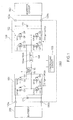
- Figure 1 is a diagram showing an example of a configuration of a power supply system 1000 according to an embodiment 1, which is an aspect of the present invention.
- the power supply system 1000 includes a bidirectional DC-DC converter 100, a battery 200 and an inverter circuit 300.
- the battery 200 is connected to a first low voltage-side input/output terminal 100a of the bidirectional DC-DC converter 100 at a positive electrode thereof and to a second low voltage-side input/output terminal 100b of the bidirectional DC-DC converter 100 at a negative electrode thereof.
- the inverter circuit 300 is connected to a first high voltage-side input/output terminal 100c and a second high voltage-side input/output terminal 100d of the bidirectional DC-DC converter 100 and is configured to perform conversion between a direct current and an alternating current.
- an alternating-current generator or a load which is not shown in the figure, is connected to the inverter circuit 300.
- the bidirectional DC-DC converter 100 has the first low voltage-side input/output terminal 100a, the second low voltage-side input/output terminal 100b, the first high voltage-side input/output terminal 100c, the second high voltage-side input/output terminal 100d, a low voltage-side rectifying circuit 101, a high voltage-side rectifying circuit 102, a controlling circuit 103, an LC resonant circuit 104, a first smoothing capacitor "C1", a second smoothing capacitor "C2" and a transformer "T", for example.
- the low voltage-side rectifying circuit 101 is connected to the first low voltage-side input/output terminal 100a and the second low voltage-side input/output terminal 100b.
- the low voltage-side rectifying circuit 101 has a first switching element "Q1", a second switching element “Q2", a third switching element “Q3” and a fourth switching element “Q4", which are n-channel MOS transistors, and a first diode “D1”, a second diode “D2”, a third diode “D3” and a fourth diode “D4", for example.
- the first switching element "Q1" is connected to the first low voltage-side input/output terminal 100a at one end thereof.
- the second switching element "Q2" is connected to the first low voltage-side input/output terminal 100a at one end thereof.
- the third switching element "Q3" is connected to the other end of the first switching element “Q1" at one end thereof and to the second low voltage-side input/output terminal 100b at the other end thereof.
- the fourth switching element "Q4" is connected to the other end of the second switching element "Q2" at one end thereof and to the second low voltage-side input/output terminal 100b at the other end thereof.
- the first diode "D1" is connected to the one end of the first switching element "Q1" at a cathode thereof and to the other end of the first switching element "Q1" at an anode thereof.
- the second diode "D2" is connected to the one end of the second switching element "Q2" at a cathode thereof and to the other end of the second switching element "Q2" at an anode thereof.
- the third diode "D3" is connected to the one end of the third switching element "Q3" at a cathode thereof and to the other end of the third switching element "Q3" at an anode thereof.
- the fourth diode "D4" is connected to the one end of the fourth switching element "Q4" at a cathode thereof and to the other end of the fourth switching element "Q4" at an anode thereof.
- the high voltage-side rectifying circuit 102 is connected to the first high voltage-side input/output terminal 100c and the second high voltage-side input/output terminal 100d.
- the high voltage-side rectifying circuit 102 has a fifth switching element "Q5", a sixth switching element “Q6", a seventh switching element “Q7” and an eighth switching element “Q8", which are n-channel MOS transistors, and a fifth diode "D5", a sixth diode “D6", a seventh diode “D7” and an eighth diode “D8", for example.
- the fifth switching element "Q5" is connected to the first high voltage-side input/output terminal 100c at one end thereof.
- the sixth switching element "Q6" is connected to the first high voltage-side input/output terminal 100c at one end thereof.
- the seventh switching element "Q7" is connected to the other end of the fifth switching element "Q5" at one end thereof and to the second high voltage-side input/output terminal 100d at the other end thereof.
- the eighth switching element "Q8" is connected to the other end of the sixth switching element "Q6" at one end thereof and to the second high voltage-side input/output terminal 100d at the other end thereof.
- the fifth diode "D5" is connected to the one end of the fifth switching element "Q5" at a cathode thereof and to the other end of the fifth switching element "Q5" at an anode thereof.
- the sixth diode "D6" is connected to the one end of the sixth switching element "Q6" at a cathode thereof and to the other end of the sixth switching element "Q6" at an anode thereof.
- the seventh diode "D7" is connected to the one end of the seventh switching element "Q7" at a cathode thereof and to the other end of the seventh switching element "Q7" at an anode thereof.
- the eighth diode "D8" is connected to the one end of the eighth switching element "Q8" at a cathode thereof and to the other end of the eighth switching element "Q8" at an anode thereof.
- the transformer “T” is connected to the low voltage-side rectifying circuit 101 and the high voltage-side rectifying circuit 102.
- the transformer “T” is homopolar.
- the transformer “T” has a first winding "T1" and a second winding "T2".
- the first winding "T1" is connected to the the other end of the first switching element "Q1" at one end thereof and to the the other end of the second switching element "Q2" at the other end thereof.
- the second winding "T2" is connected to the the other end of the fifth switching element "Q5" at one end thereof and to the other end of the sixth switching element "Q6" at the other end thereof.
- the number of turns of the second winding "T2" is set to be greater than the number of turns of the first winding "T1".
- the LC resonant circuit 104 is connected between the other end of the second winding "T2" and the other end of the sixth switching element "Q6".
- the LC resonant circuit 104 has a resonant capacitor 104a connected to the other end of the second winding "T2" at one end thereof and a choke coil 104b connected to the other end of the resonant capacitor 104a at one end thereof and to the other end of the sixth switching element "Q6" at the other end thereof, for example.
- the first smoothing capacitor "C1" is connected between the first low voltage-side input/output terminal 100a and the second low voltage-side input/output terminal 100b and is configured to smooth the voltage between the first low voltage-side input/output terminal 100a and the second low voltage-side input/output terminal 100b.
- the second smoothing capacitor "C2" is connected between the first high voltage-side input/output terminal 100c and the second high voltage-side input/output terminal 100d and is configured to smooth the voltage between the first high voltage-side input/output terminal 100c and the second high voltage-side input/output terminal 100d.
- the controlling circuit 103 is configured to control operations of the switching elements "Q1" to "Q8" in the low voltage-side rectifying circuit 101 and the high voltage-side rectifying circuit 102. More specifically, the controlling circuit 103 applies a controlling signal to gates of the MOS transistors serving as the first to eighth switching elements “Q1” to “Q8", thereby controls turning on and off of the first to eighth switching elements (MOS transistors) "Q1" to "Q8".
- the controlling circuit 103 is configured to achieve soft switching of the switching elements in the high voltage-side rectifying circuit 102 in a step-down operation (that is, a state where the inverter circuit 300 is connected to the alternating-current generator and is supplied with electricity), for example, as described later.
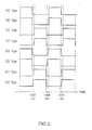
- Figure 2 is a waveform diagram showing examples of controlling signals input to the gates of the MOS transistors in the low voltage-side rectifying circuit 101 and the high voltage-side rectifying circuit 102 in the bidirectional DC-DC converter 100 shown in Figure 1 in the step-down operation.
- the controlling circuit 103 sets controlling signals (voltages applied to the gates of each of the n-channel MOS transistors) "Q1Vgs" to “Q8Vgs" at a "Low” level. In this way, the controlling circuit 103 turns off the first to eighth switching elements "Q1" to "Q8".
- the controlling circuit 103 sets the controlling signal "Q1Vgs" and “Q4Vgs” at a "High” level from the state described above, thereby turning on the first and fourth switching elements "Q1" and "Q4" in the low voltage-side rectifying circuit 101.
- the controlling circuit 103 sets the controlling signal "Q6Vgs" and “Q7Vgs” at the "High” level, thereby turning on the sixth and seventh switching elements "Q6" and "Q7” in the high voltage-side rectifying circuit 102.
- the first and fourth switching elements "Q1" and “Q4" in the low voltage-side rectifying circuit 101 are turned on earlier than the sixth and seventh switching element “Q6" and “Q7” in the high voltage-side rectifying circuit 102 (the voltage of the battery that is originally output is inverse-transformed through the first and fourth switching elements “Q1” and “Q4" and the first winding "T1" toward the second winding "T2".
- the drain-source voltage "Vds" becomes 0 V earlier than the gate signal, and the soft switching operation is processed).
- the converter efficiency is improved, occurrence of noise is reduced, and breakdown of the switching elements can be prevented.
- the controlling circuit 103 sets the controlling signals "Q1vgs", “Q4Vgs”, “Q6Vgs” and “Q7Vgs” at the "Low” level, thereby turning off the first, fourth, sixth and seventh switching elements "Q1", “Q4", "Q6” and "Q7".
- the controlling circuit 103 sets the controlling signal "Q2Vgs" and “Q3Vgs” at the "High” level, thereby turning on the second and third switching elements "Q2" and “Q3" in the low voltage-side rectifying circuit 101.
- the controlling circuit 103 sets the controlling signal "Q5Vgs” and “Q8Vgs” at the "High” level, thereby turning on the fifth and eighth switching elements "Q5" and "Q8" in the high voltage-side rectifying circuit 102.
- the second and third switching elements "Q2" and “Q3" in the low voltage-side rectifying circuit 101 are turned on earlier than the fifth and eighth switching element "Q5" and “Q8” in the high voltage-side rectifying circuit 102 (the voltage of the battery that is originally output is inverse-transformed through the second and third switching elements “Q2" and “Q3” and the first winding "T1" toward the second winding "T2".
- the drain-source voltage "Vds" becomes 0 V earlier than the gate signal, and the soft switching operation is processed).
- the converter efficiency is improved, occurrence of noise is reduced, and breakdown of the switching elements can be prevented.
- the controlling circuit 103 sets the controlling signals "Q2Vgs", “Q3Vgs”, “Q5Vgs” and “Q8Vgs” at the "Low” level, thereby turning off the second, third, fifth and eighth switching elements "Q2", “Q3", “Q5" and “Q8".
- the controlling circuit 103 sets the controlling signal "Q1Vgs” and “Q4Vgs” at the "High” level, thereby turning on the first and fourth switching elements "Q1" and "Q4" in the low voltage-side rectifying circuit 101.
- the controlling circuit 103 sets the controlling signal "Q6Vgs" and “Q7Vgs” at the "High” level, thereby turning on the sixth and seventh switching elements "Q6" and "Q7” in the high voltage-side rectifying circuit 102.
- the first and fourth switching elements "Q1" and “Q4" in the low voltage-side rectifying circuit 101 are turned on earlier than the sixth and seventh switching element “Q6" and “Q7” in the high voltage-side rectifying circuit 102 (the voltage of the battery that is originally output is inverse-transformed through the first and fourth switching elements “Q1” and “Q4" and the first winding "T1" toward the second winding "T2".
- the drain-source voltage "Vds" becomes 0 V earlier than the gate signal, and the soft switching operation is processed).
- the converter efficiency is improved, occurrence of noise is reduced, and breakdown of the switching elements can be prevented.
- the controlling circuit 103 achieves soft switching of the MOS transistors serving as the switching elements in the high voltage-side rectifying circuit 102.
- the bidirectional DC-DC converter 100 can achieve switching by more appropriate partial voltage resonance.
- the converter efficiency of the bidirectional DC-DC converter 100 is improved, occurrence of noise is reduced, and breakdown of the switching elements can be prevented.
- the switching elements are n-channel MOS transistors
- the same description holds true for a case where the switching elements are p-channel MOS transistors.
Landscapes
- Engineering & Computer Science (AREA)
- Power Engineering (AREA)
- Dc-Dc Converters (AREA)
Applications Claiming Priority (2)
| Application Number | Priority Date | Filing Date | Title |
|---|---|---|---|
| JP2011049347 | 2011-03-07 | ||
| PCT/JP2012/054326 WO2012121016A1 (ja) | 2011-03-07 | 2012-02-22 | 双方向dc-dcコンバータ、および、電源システム |
Publications (3)
| Publication Number | Publication Date |
|---|---|
| EP2685620A1 true EP2685620A1 (de) | 2014-01-15 |
| EP2685620A4 EP2685620A4 (de) | 2014-12-03 |
| EP2685620B1 EP2685620B1 (de) | 2017-08-16 |
Family
ID=46797985
Family Applications (1)
| Application Number | Title | Priority Date | Filing Date |
|---|---|---|---|
| EP12754309.8A Active EP2685620B1 (de) | 2011-03-07 | 2012-02-22 | Bidirektionaler gleichspannungswandler und stromquellensystem |
Country Status (4)
| Country | Link |
|---|---|
| US (1) | US9112423B2 (de) |
| EP (1) | EP2685620B1 (de) |
| JP (1) | JP5437530B2 (de) |
| WO (1) | WO2012121016A1 (de) |
Cited By (3)
| Publication number | Priority date | Publication date | Assignee | Title |
|---|---|---|---|---|
| CN106208710A (zh) * | 2016-07-15 | 2016-12-07 | 江苏固德威电源科技股份有限公司 | 一种双向dc‑dc转换器及控制方法 |
| CN109412420A (zh) * | 2018-11-08 | 2019-03-01 | 江苏固德威电源科技股份有限公司 | 双向隔离dc/dc电路及其采用的控制方法 |
| EP3509203A1 (de) * | 2018-01-09 | 2019-07-10 | Infineon Technologies Austria AG | Umrichter mit nullspannungsschaltung |
Families Citing this family (11)
| Publication number | Priority date | Publication date | Assignee | Title |
|---|---|---|---|---|
| JP5987980B2 (ja) * | 2013-05-30 | 2016-09-07 | 日産自動車株式会社 | 位相制御型dc−dcコンバータおよびその制御方法 |
| JP6157388B2 (ja) * | 2014-03-13 | 2017-07-05 | 三菱電機株式会社 | 双方向dcdcコンバータ |
| EP2924863A1 (de) * | 2014-03-27 | 2015-09-30 | Kone Corporation | Bidirektionale Schaltnetzteilversorgung |
| KR102421163B1 (ko) * | 2015-05-19 | 2022-07-14 | 엘지이노텍 주식회사 | 양방향 직류-직류 컨버터 |
| US9602011B1 (en) * | 2015-12-28 | 2017-03-21 | Harman International Industries, Incorporated | Gated bi-directional dual-rail series resonant converter power supply |
| US11411510B2 (en) * | 2020-01-24 | 2022-08-09 | Lear Corporation | DC/AC inverter resonance topology |
| JP7449259B2 (ja) * | 2021-03-29 | 2024-03-13 | パナソニックホールディングス株式会社 | 電力変換装置、電力変換システム、制御方法及びプログラム |
| CN115720045B (zh) * | 2021-08-24 | 2026-02-17 | 中山旭贵明电子有限公司 | 可升降压的双向直流-直流电源转换装置及其控制方法 |
| JP7779110B2 (ja) * | 2021-11-29 | 2025-12-03 | オムロン株式会社 | 電力変換装置 |
| CN116633160B (zh) * | 2023-07-26 | 2023-09-26 | 南京航空航天大学 | 单级式隔离型双向/单向dc-dc变换器及控制方法 |
| CN122315843A (zh) * | 2024-12-26 | 2026-06-30 | 香港理工大学 | 供电电路及供电设备 |
Family Cites Families (7)
| Publication number | Priority date | Publication date | Assignee | Title |
|---|---|---|---|---|
| JP2002165448A (ja) | 2000-11-20 | 2002-06-07 | Denso Corp | 双方向dc−dcコンバータ |
| JP4274353B2 (ja) * | 2003-03-13 | 2009-06-03 | 本田技研工業株式会社 | 双方向dc−dcコンバータ |
| JP2005168167A (ja) * | 2003-12-02 | 2005-06-23 | Honda Motor Co Ltd | Dc−dcコンバータ |
| JP4274364B2 (ja) * | 2004-02-05 | 2009-06-03 | 本田技研工業株式会社 | Dc−dcコンバータ |
| JP4454444B2 (ja) | 2004-09-08 | 2010-04-21 | 本田技研工業株式会社 | 双方向dc−dcコンバータ |
| JP4527616B2 (ja) | 2005-06-24 | 2010-08-18 | 株式会社日立製作所 | 絶縁共振形双方向dc/dcコンバータ及びその制御方法 |
| US20110149611A1 (en) * | 2009-12-21 | 2011-06-23 | Intersil Americas Inc. | Bidirectional signal conversion |
-
2012
- 2012-02-22 JP JP2013503447A patent/JP5437530B2/ja active Active
- 2012-02-22 EP EP12754309.8A patent/EP2685620B1/de active Active
- 2012-02-22 US US14/002,370 patent/US9112423B2/en active Active
- 2012-02-22 WO PCT/JP2012/054326 patent/WO2012121016A1/ja not_active Ceased
Non-Patent Citations (2)
| Title |
|---|
| Nikolaus Schibli: "Symmetrical Multilevel Converters with Two Quadrant DC-DC Feeding", , 15 September 2000 (2000-09-15), XP055147771, Lausanne DOI: 10.5075/epfl-thesis-2220 Retrieved from the Internet: URL:http://infoscience.epfl.ch/record/32696/files/EPFL_TH2220.pdf [retrieved on 2014-10-20] * |
| See also references of WO2012121016A1 * |
Cited By (6)
| Publication number | Priority date | Publication date | Assignee | Title |
|---|---|---|---|---|
| CN106208710A (zh) * | 2016-07-15 | 2016-12-07 | 江苏固德威电源科技股份有限公司 | 一种双向dc‑dc转换器及控制方法 |
| CN106208710B (zh) * | 2016-07-15 | 2019-01-25 | 江苏固德威电源科技股份有限公司 | 一种双向dc-dc转换器的控制方法 |
| EP3509203A1 (de) * | 2018-01-09 | 2019-07-10 | Infineon Technologies Austria AG | Umrichter mit nullspannungsschaltung |
| US10389275B2 (en) | 2018-01-09 | 2019-08-20 | Infineon Technologies Austria Ag | Converter with ZVS |
| CN109412420A (zh) * | 2018-11-08 | 2019-03-01 | 江苏固德威电源科技股份有限公司 | 双向隔离dc/dc电路及其采用的控制方法 |
| WO2020093508A1 (zh) * | 2018-11-08 | 2020-05-14 | 江苏固德威电源科技股份有限公司 | 双向隔离dc/dc电路及其采用的控制方法 |
Also Published As
| Publication number | Publication date |
|---|---|
| JP5437530B2 (ja) | 2014-03-12 |
| WO2012121016A1 (ja) | 2012-09-13 |
| US20130343093A1 (en) | 2013-12-26 |
| JPWO2012121016A1 (ja) | 2014-07-17 |
| EP2685620B1 (de) | 2017-08-16 |
| EP2685620A4 (de) | 2014-12-03 |
| US9112423B2 (en) | 2015-08-18 |
Similar Documents
| Publication | Publication Date | Title |
|---|---|---|
| US9112423B2 (en) | Bidirectional DC-DC converter and power supply system | |
| US11909326B2 (en) | Parallel hybrid converter apparatus and method | |
| CN105191100B (zh) | 双向dc/dc转换器 | |
| JP4844674B2 (ja) | スイッチング電源装置 | |
| US9461554B2 (en) | Hybrid converter using a resonant stage and a non-isolated stage | |
| US9350260B2 (en) | Startup method and system for resonant converters | |
| US20080074905A1 (en) | Method for Controlling Bidirectional DC-DC Converter | |
| US20230113753A1 (en) | Dc/dc converter and method for controlling output voltage thereof | |
| JP6241334B2 (ja) | 電流共振型dcdcコンバータ | |
| US8064228B2 (en) | Power supply apparatus with current-sharing function | |
| US20120044729A1 (en) | Bridgeless coupled inductor boost power factor rectifiers | |
| WO2013073173A1 (ja) | バッテリ充電装置 | |
| US9564819B2 (en) | Switching power supply circuit | |
| US20200389094A1 (en) | Power supply device | |
| EP2680423B1 (de) | Synchrongleichrichtungsvorrichtung und netzteil mit synchrongleichrichtung | |
| US10199867B2 (en) | Power conversion device and wireless power transmission system | |
| JP2006191706A (ja) | 直流変換装置 | |
| EP3869681A1 (de) | Stromversorgungsvorrichtung | |
| KR102525753B1 (ko) | 절연형 스위칭 전원 공급 장치 | |
| JP6945429B2 (ja) | 絶縁型スイッチング電源 | |
| US9673716B2 (en) | Resonant converter with three switches | |
| KR102537358B1 (ko) | 절연형 스위칭 전원 | |
| US12519397B2 (en) | Switching power supply apparatus and electric power supply system | |
| JP4265199B2 (ja) | 直流変換装置 | |
| EP4009503A1 (de) | Spannungswandlungsvorrichtung |
Legal Events
| Date | Code | Title | Description |
|---|---|---|---|
| PUAI | Public reference made under article 153(3) epc to a published international application that has entered the european phase |
Free format text: ORIGINAL CODE: 0009012 |
|
| 17P | Request for examination filed |
Effective date: 20130705 |
|
| AK | Designated contracting states |
Kind code of ref document: A1 Designated state(s): AL AT BE BG CH CY CZ DE DK EE ES FI FR GB GR HR HU IE IS IT LI LT LU LV MC MK MT NL NO PL PT RO RS SE SI SK SM TR |
|
| DAX | Request for extension of the european patent (deleted) | ||
| A4 | Supplementary search report drawn up and despatched |
Effective date: 20141105 |
|
| RIC1 | Information provided on ipc code assigned before grant |
Ipc: H02M 3/335 20060101AFI20141030BHEP Ipc: H02M 3/337 20060101ALI20141030BHEP Ipc: H02M 1/00 20070101ALI20141030BHEP |
|
| REG | Reference to a national code |
Ref country code: DE Ref legal event code: R079 Ref document number: 602012036010 Country of ref document: DE Free format text: PREVIOUS MAIN CLASS: H02M0003280000 Ipc: H02M0003335000 |
|
| GRAP | Despatch of communication of intention to grant a patent |
Free format text: ORIGINAL CODE: EPIDOSNIGR1 |
|
| RIC1 | Information provided on ipc code assigned before grant |
Ipc: H02M 3/335 20060101AFI20170208BHEP Ipc: H02M 1/00 20070101ALI20170208BHEP Ipc: H02M 3/337 20060101ALI20170208BHEP |
|
| INTG | Intention to grant announced |
Effective date: 20170303 |
|
| GRAS | Grant fee paid |
Free format text: ORIGINAL CODE: EPIDOSNIGR3 |
|
| GRAA | (expected) grant |
Free format text: ORIGINAL CODE: 0009210 |
|
| AK | Designated contracting states |
Kind code of ref document: B1 Designated state(s): AL AT BE BG CH CY CZ DE DK EE ES FI FR GB GR HR HU IE IS IT LI LT LU LV MC MK MT NL NO PL PT RO RS SE SI SK SM TR |
|
| REG | Reference to a national code |
Ref country code: GB Ref legal event code: FG4D |
|
| REG | Reference to a national code |
Ref country code: CH Ref legal event code: EP |
|
| REG | Reference to a national code |
Ref country code: IE Ref legal event code: FG4D |
|
| REG | Reference to a national code |
Ref country code: AT Ref legal event code: REF Ref document number: 919984 Country of ref document: AT Kind code of ref document: T Effective date: 20170915 |
|
| REG | Reference to a national code |
Ref country code: DE Ref legal event code: R096 Ref document number: 602012036010 Country of ref document: DE |
|
| REG | Reference to a national code |
Ref country code: NL Ref legal event code: MP Effective date: 20170816 |
|
| REG | Reference to a national code |
Ref country code: LT Ref legal event code: MG4D |
|
| REG | Reference to a national code |
Ref country code: AT Ref legal event code: MK05 Ref document number: 919984 Country of ref document: AT Kind code of ref document: T Effective date: 20170816 |
|
| PG25 | Lapsed in a contracting state [announced via postgrant information from national office to epo] |
Ref country code: AT Free format text: LAPSE BECAUSE OF FAILURE TO SUBMIT A TRANSLATION OF THE DESCRIPTION OR TO PAY THE FEE WITHIN THE PRESCRIBED TIME-LIMIT Effective date: 20170816 Ref country code: FI Free format text: LAPSE BECAUSE OF FAILURE TO SUBMIT A TRANSLATION OF THE DESCRIPTION OR TO PAY THE FEE WITHIN THE PRESCRIBED TIME-LIMIT Effective date: 20170816 Ref country code: SE Free format text: LAPSE BECAUSE OF FAILURE TO SUBMIT A TRANSLATION OF THE DESCRIPTION OR TO PAY THE FEE WITHIN THE PRESCRIBED TIME-LIMIT Effective date: 20170816 Ref country code: NL Free format text: LAPSE BECAUSE OF FAILURE TO SUBMIT A TRANSLATION OF THE DESCRIPTION OR TO PAY THE FEE WITHIN THE PRESCRIBED TIME-LIMIT Effective date: 20170816 Ref country code: NO Free format text: LAPSE BECAUSE OF FAILURE TO SUBMIT A TRANSLATION OF THE DESCRIPTION OR TO PAY THE FEE WITHIN THE PRESCRIBED TIME-LIMIT Effective date: 20171116 Ref country code: LT Free format text: LAPSE BECAUSE OF FAILURE TO SUBMIT A TRANSLATION OF THE DESCRIPTION OR TO PAY THE FEE WITHIN THE PRESCRIBED TIME-LIMIT Effective date: 20170816 |
|
| PG25 | Lapsed in a contracting state [announced via postgrant information from national office to epo] |
Ref country code: GR Free format text: LAPSE BECAUSE OF FAILURE TO SUBMIT A TRANSLATION OF THE DESCRIPTION OR TO PAY THE FEE WITHIN THE PRESCRIBED TIME-LIMIT Effective date: 20171117 Ref country code: IS Free format text: LAPSE BECAUSE OF FAILURE TO SUBMIT A TRANSLATION OF THE DESCRIPTION OR TO PAY THE FEE WITHIN THE PRESCRIBED TIME-LIMIT Effective date: 20171216 Ref country code: LV Free format text: LAPSE BECAUSE OF FAILURE TO SUBMIT A TRANSLATION OF THE DESCRIPTION OR TO PAY THE FEE WITHIN THE PRESCRIBED TIME-LIMIT Effective date: 20170816 Ref country code: BG Free format text: LAPSE BECAUSE OF FAILURE TO SUBMIT A TRANSLATION OF THE DESCRIPTION OR TO PAY THE FEE WITHIN THE PRESCRIBED TIME-LIMIT Effective date: 20171116 Ref country code: RS Free format text: LAPSE BECAUSE OF FAILURE TO SUBMIT A TRANSLATION OF THE DESCRIPTION OR TO PAY THE FEE WITHIN THE PRESCRIBED TIME-LIMIT Effective date: 20170816 Ref country code: ES Free format text: LAPSE BECAUSE OF FAILURE TO SUBMIT A TRANSLATION OF THE DESCRIPTION OR TO PAY THE FEE WITHIN THE PRESCRIBED TIME-LIMIT Effective date: 20170816 Ref country code: PL Free format text: LAPSE BECAUSE OF FAILURE TO SUBMIT A TRANSLATION OF THE DESCRIPTION OR TO PAY THE FEE WITHIN THE PRESCRIBED TIME-LIMIT Effective date: 20170816 |
|
| PG25 | Lapsed in a contracting state [announced via postgrant information from national office to epo] |
Ref country code: RO Free format text: LAPSE BECAUSE OF FAILURE TO SUBMIT A TRANSLATION OF THE DESCRIPTION OR TO PAY THE FEE WITHIN THE PRESCRIBED TIME-LIMIT Effective date: 20170816 Ref country code: DK Free format text: LAPSE BECAUSE OF FAILURE TO SUBMIT A TRANSLATION OF THE DESCRIPTION OR TO PAY THE FEE WITHIN THE PRESCRIBED TIME-LIMIT Effective date: 20170816 Ref country code: CZ Free format text: LAPSE BECAUSE OF FAILURE TO SUBMIT A TRANSLATION OF THE DESCRIPTION OR TO PAY THE FEE WITHIN THE PRESCRIBED TIME-LIMIT Effective date: 20170816 |
|
| REG | Reference to a national code |
Ref country code: DE Ref legal event code: R097 Ref document number: 602012036010 Country of ref document: DE |
|
| PG25 | Lapsed in a contracting state [announced via postgrant information from national office to epo] |
Ref country code: IT Free format text: LAPSE BECAUSE OF FAILURE TO SUBMIT A TRANSLATION OF THE DESCRIPTION OR TO PAY THE FEE WITHIN THE PRESCRIBED TIME-LIMIT Effective date: 20170816 Ref country code: SM Free format text: LAPSE BECAUSE OF FAILURE TO SUBMIT A TRANSLATION OF THE DESCRIPTION OR TO PAY THE FEE WITHIN THE PRESCRIBED TIME-LIMIT Effective date: 20170816 Ref country code: EE Free format text: LAPSE BECAUSE OF FAILURE TO SUBMIT A TRANSLATION OF THE DESCRIPTION OR TO PAY THE FEE WITHIN THE PRESCRIBED TIME-LIMIT Effective date: 20170816 Ref country code: SK Free format text: LAPSE BECAUSE OF FAILURE TO SUBMIT A TRANSLATION OF THE DESCRIPTION OR TO PAY THE FEE WITHIN THE PRESCRIBED TIME-LIMIT Effective date: 20170816 |
|
| PLBE | No opposition filed within time limit |
Free format text: ORIGINAL CODE: 0009261 |
|
| STAA | Information on the status of an ep patent application or granted ep patent |
Free format text: STATUS: NO OPPOSITION FILED WITHIN TIME LIMIT |
|
| 26N | No opposition filed |
Effective date: 20180517 |
|
| PG25 | Lapsed in a contracting state [announced via postgrant information from national office to epo] |
Ref country code: SI Free format text: LAPSE BECAUSE OF FAILURE TO SUBMIT A TRANSLATION OF THE DESCRIPTION OR TO PAY THE FEE WITHIN THE PRESCRIBED TIME-LIMIT Effective date: 20170816 |
|
| REG | Reference to a national code |
Ref country code: CH Ref legal event code: PL |
|
| PG25 | Lapsed in a contracting state [announced via postgrant information from national office to epo] |
Ref country code: MC Free format text: LAPSE BECAUSE OF FAILURE TO SUBMIT A TRANSLATION OF THE DESCRIPTION OR TO PAY THE FEE WITHIN THE PRESCRIBED TIME-LIMIT Effective date: 20170816 |
|
| GBPC | Gb: european patent ceased through non-payment of renewal fee |
Effective date: 20180222 |
|
| REG | Reference to a national code |
Ref country code: IE Ref legal event code: MM4A |
|
| REG | Reference to a national code |
Ref country code: BE Ref legal event code: MM Effective date: 20180228 |
|
| PG25 | Lapsed in a contracting state [announced via postgrant information from national office to epo] |
Ref country code: LU Free format text: LAPSE BECAUSE OF NON-PAYMENT OF DUE FEES Effective date: 20180222 Ref country code: LI Free format text: LAPSE BECAUSE OF NON-PAYMENT OF DUE FEES Effective date: 20180228 Ref country code: CH Free format text: LAPSE BECAUSE OF NON-PAYMENT OF DUE FEES Effective date: 20180228 |
|
| REG | Reference to a national code |
Ref country code: FR Ref legal event code: ST Effective date: 20181031 |
|
| PG25 | Lapsed in a contracting state [announced via postgrant information from national office to epo] |
Ref country code: IE Free format text: LAPSE BECAUSE OF NON-PAYMENT OF DUE FEES Effective date: 20180222 |
|
| PG25 | Lapsed in a contracting state [announced via postgrant information from national office to epo] |
Ref country code: GB Free format text: LAPSE BECAUSE OF NON-PAYMENT OF DUE FEES Effective date: 20180222 Ref country code: FR Free format text: LAPSE BECAUSE OF NON-PAYMENT OF DUE FEES Effective date: 20180228 Ref country code: BE Free format text: LAPSE BECAUSE OF NON-PAYMENT OF DUE FEES Effective date: 20180228 |
|
| PG25 | Lapsed in a contracting state [announced via postgrant information from national office to epo] |
Ref country code: MT Free format text: LAPSE BECAUSE OF NON-PAYMENT OF DUE FEES Effective date: 20180222 |
|
| PG25 | Lapsed in a contracting state [announced via postgrant information from national office to epo] |
Ref country code: TR Free format text: LAPSE BECAUSE OF FAILURE TO SUBMIT A TRANSLATION OF THE DESCRIPTION OR TO PAY THE FEE WITHIN THE PRESCRIBED TIME-LIMIT Effective date: 20170816 |
|
| PG25 | Lapsed in a contracting state [announced via postgrant information from national office to epo] |
Ref country code: PT Free format text: LAPSE BECAUSE OF FAILURE TO SUBMIT A TRANSLATION OF THE DESCRIPTION OR TO PAY THE FEE WITHIN THE PRESCRIBED TIME-LIMIT Effective date: 20170816 Ref country code: HU Free format text: LAPSE BECAUSE OF FAILURE TO SUBMIT A TRANSLATION OF THE DESCRIPTION OR TO PAY THE FEE WITHIN THE PRESCRIBED TIME-LIMIT; INVALID AB INITIO Effective date: 20120222 |
|
| PG25 | Lapsed in a contracting state [announced via postgrant information from national office to epo] |
Ref country code: HR Free format text: LAPSE BECAUSE OF FAILURE TO SUBMIT A TRANSLATION OF THE DESCRIPTION OR TO PAY THE FEE WITHIN THE PRESCRIBED TIME-LIMIT Effective date: 20170816 Ref country code: CY Free format text: LAPSE BECAUSE OF FAILURE TO SUBMIT A TRANSLATION OF THE DESCRIPTION OR TO PAY THE FEE WITHIN THE PRESCRIBED TIME-LIMIT Effective date: 20170816 Ref country code: MK Free format text: LAPSE BECAUSE OF NON-PAYMENT OF DUE FEES Effective date: 20170816 |
|
| PG25 | Lapsed in a contracting state [announced via postgrant information from national office to epo] |
Ref country code: AL Free format text: LAPSE BECAUSE OF FAILURE TO SUBMIT A TRANSLATION OF THE DESCRIPTION OR TO PAY THE FEE WITHIN THE PRESCRIBED TIME-LIMIT Effective date: 20170816 |
|
| PGFP | Annual fee paid to national office [announced via postgrant information from national office to epo] |
Ref country code: DE Payment date: 20260218 Year of fee payment: 15 |