EP2685630A1 - Zweistufiger rauscharmer Verstärker mit Eintakteingang und Differenzausgangsstromwiederverwendung - Google Patents
Zweistufiger rauscharmer Verstärker mit Eintakteingang und Differenzausgangsstromwiederverwendung Download PDFInfo
- Publication number
- EP2685630A1 EP2685630A1 EP12176475.7A EP12176475A EP2685630A1 EP 2685630 A1 EP2685630 A1 EP 2685630A1 EP 12176475 A EP12176475 A EP 12176475A EP 2685630 A1 EP2685630 A1 EP 2685630A1
- Authority
- EP
- European Patent Office
- Prior art keywords
- stage
- low noise
- noise amplifier
- gain stage
- current reuse
- Prior art date
- Legal status (The legal status is an assumption and is not a legal conclusion. Google has not performed a legal analysis and makes no representation as to the accuracy of the status listed.)
- Granted
Links
Images



Classifications
-
- H—ELECTRICITY
- H03—ELECTRONIC CIRCUITRY
- H03F—AMPLIFIERS
- H03F1/00—Details of amplifiers with only discharge tubes, only semiconductor devices or only unspecified devices as amplifying elements
- H03F1/02—Modifications of amplifiers to raise the efficiency, e.g. gliding Class A stages, use of an auxiliary oscillation
- H03F1/0205—Modifications of amplifiers to raise the efficiency, e.g. gliding Class A stages, use of an auxiliary oscillation in transistor amplifiers
- H03F1/0283—Reducing the number of DC-current paths
-
- H—ELECTRICITY
- H03—ELECTRONIC CIRCUITRY
- H03F—AMPLIFIERS
- H03F1/00—Details of amplifiers with only discharge tubes, only semiconductor devices or only unspecified devices as amplifying elements
- H03F1/08—Modifications of amplifiers to reduce detrimental influences of internal impedances of amplifying elements
- H03F1/22—Modifications of amplifiers to reduce detrimental influences of internal impedances of amplifying elements by use of cascode coupling, i.e. earthed cathode or emitter stage followed by earthed grid or base stage respectively
- H03F1/223—Modifications of amplifiers to reduce detrimental influences of internal impedances of amplifying elements by use of cascode coupling, i.e. earthed cathode or emitter stage followed by earthed grid or base stage respectively with MOSFET's
-
- H—ELECTRICITY
- H03—ELECTRONIC CIRCUITRY
- H03F—AMPLIFIERS
- H03F3/00—Amplifiers with only discharge tubes or only semiconductor devices as amplifying elements
- H03F3/45—Differential amplifiers
- H03F3/45071—Differential amplifiers with semiconductor devices only
- H03F3/45076—Differential amplifiers with semiconductor devices only characterised by the way of implementation of the active amplifying circuit in the differential amplifier
- H03F3/45179—Differential amplifiers with semiconductor devices only characterised by the way of implementation of the active amplifying circuit in the differential amplifier using MOSFET transistors as the active amplifying circuit
- H03F3/45183—Long tailed pairs
- H03F3/45188—Non-folded cascode stages
-
- H—ELECTRICITY
- H03—ELECTRONIC CIRCUITRY
- H03F—AMPLIFIERS
- H03F2200/00—Indexing scheme relating to amplifiers
- H03F2200/294—Indexing scheme relating to amplifiers the amplifier being a low noise amplifier [LNA]
-
- H—ELECTRICITY
- H03—ELECTRONIC CIRCUITRY
- H03F—AMPLIFIERS
- H03F2203/00—Indexing scheme relating to amplifiers with only discharge tubes or only semiconductor devices as amplifying elements covered by H03F3/00
- H03F2203/45—Indexing scheme relating to differential amplifiers
- H03F2203/45652—Indexing scheme relating to differential amplifiers the LC comprising one or more further dif amp stages, either identical to the dif amp or not, in cascade
Definitions
- the present invention concerns a current-reuse low noise amplifier and an integrated circuit comprising this amplifier.
- the design of the radio frequency (RF) front-end circuit is nowadays of primary importance for the good performance of a transceiver radio link.
- radio-frequency indicates the range of frequencies between 3 kHz and 300 GHz, in particular between 300 MHz and 6 GHz.
- the transceiver can for example be used as part of a wireless sensor node, a medical device (hearing aids, insulin pump control, pace-maker, etc), a device for a body area network (BAN), a high performance receiver for GPS applications, etc.
- the first block of the receiver could be an amplifier, named low-noise amplifier or LNA.
- LNA low-noise amplifier
- the total noise of a receiver is mainly determined by the noise and gain of its first block, i.e. the LNA, the noise of the next blocks referred to the input of the receiver being proportionally less significant since reduced by the gain of the preceding blocks.
- the LNA could be followed by a mixer for translating the frequency of the received signal from the RF frequency to a lower frequency, named intermediated frequency or IF.
- the mixer In the case of a direct conversion architecture of the receiver, the mixer translates the received signal in the base band.
- the low noise amplifier could be a double-ended or differential amplifier. In this case, it amplifies the difference between two input voltages or currents. This solution in fact is commonly used since it allows the rejection of the common mode disturbances, and a better linearity of the second order, not only of the LNA but also of the overall receiving chain which in general handles differential signals.
- the single-ended signal to differential signal conversion can be done in numerous ways, either by capacitive coupling or by magnetic coupling while assuring a phase shift of 180° between the original single-ended signal and the generated opposite signal.
- a possible and simple implementation is to apply the single ended signal on one input of a differential amplifier while AC-coupling the opposite input to ground. It is also possible to couple two half differential amplifiers and use passive components to guarantee the symmetry.
- balun comprising for example an inductive transformer, to generate the differential signals before applying them to the differential LNA.
- the balun is in general an external element, which is not integrated in the circuit comprising the receiving chain. It is in general placed between the SAW filter and the LNA, if the SAW filter has single ended input and output ports.
- balun as integrated element entails a degradation of the noise performance since losses are generated at the receiver input. Moreover its realization requires a substantial increase of layout-area.
- Another possibility is to use a SAW filter which performs the single-ended to differential transformation at the same time as it performs the filtering.
- the low noise amplifier could have a current reuse topology with two stages.
- current reuse means that the first and second gain stages are stacked such that the same DC current between the supply rails Vsupply and ground is used for both of them.
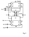
- FIG. 1 An embodiment of this kind of amplifier is shown in Figure 1 .
- a first amplifying or gain stage comprising the transistors M1 to M4 and the center-tapped differential inductance L1 comprising two magnetically coupled inductances L1' and L1" with common center tap, has a differential input IN1, IN2 and an output resonating around the common mode node Vcom.
- the output of this first gain stage is capacitively coupled to a second amplifying or gain stage comprising the transistors M5' to M8' and the center-tapped differential inductance L2 comprising two magnetically coupled inductances L2' and L2" with common center tap.
- the output of the second gain stage resonates around the upper supply voltage Vsupply.
- the transistors M3, M4, M5' and M6' act as current buffers and are named in the following cascode transistors. As known, they allow higher input-output isolation, higher input and output impedances, and the reduction or elimination of the Miller effect and thus a higher bandwidth of the LNA.
- an active differential pair as input of the low noise amplifier has different drawbacks: first, the noise sources are doubled compared to the single-ended gain stage. Moreover it is often necessary to use some supplementary element, such as a balun, a single-differential SAW filter or any other passive transforming element.
- a differential amplifier Since a differential amplifier has two transconductance branches, it requires twice the DC current of a single-ended amplifier to generate the same overall transconductance. Since the input referred noise generated by the low noise amplifier itself is inversely proportional to the transconductance of the gain stages, equal noise power referred to the input requires a factor of two more current in the differential version to obtain the same noise performance as the single ended version.
- the low noise amplifier having a differential input stage does not allow a direct connection to a single-ended antenna. Moreover the integrated circuit comprising such amplifier requires one more pin compared to a single-ended amplifier, and thus a supplementary RF port.
- a differential amplifier or at least its differential output allows reduced problems in terms of common mode disturbances and linearity of the second order for the receiving chain.
- Another aim of the present invention is to improve the current consumption of an amplifier by maintaining at least its output differential.
- Another aim of the present invention is to avoid the use of external elements for performing the single to differential transformation.
- Another aim of the present invention is then to overcome the limitation of the maximum output voltage swing for a two stage stacked or current reuse low noise amplifier.
- the current reuse low noise amplifier comprises a first gain stage with a resonant load and a second gain stage connected to the first gain stage by a capacitive coupling.
- the capacitive coupling is an AC-capacitive coupling which allows a signal connection between the first and the second gain stage.
- the first gain stage is a single-ended stage
- the second stage is a double-ended stage and the magnetic coupling within the resonant load of the first gain stage performs the single-ended to differential signal transformation between the first and the second gain stage.
- the single-ended first stage allows a current reduction in the amplifier, while maintaining its performance in terms of the input referred noise: in fact the current required for a differential first stage is twice the current required for a single-ended first stage for the same input referred noise performance. Otherwise it allows a better performance in terms of noise and sensitivity at a constant current consumption compared to a differential first stage.
- the single-ended first stage allows also a possible direct connection to a single-ended antenna, a reduction of the number of pin of the integrated circuit comprising this amplifier and a possible reduction of the size of its package.
- the resonant load of the first gain stage advantageously can comprise a center-tapped differential inductance or in other words two magnetically coupled inductances with common center tap, one of them being connected to the first gain stage and carrying the DC current, the other generating the 180° phase-shifted differential signal and being an open circuit for DC currents.
- the center-tapped differential inductance allows the coupling to the second gain working as a resonant auto-transformer with single-ended input and differential output.
- the center-tapped differential inductance is working as a resonant auto-transformer with single-ended input and differential output.
- the AC coupling between the two gain stages is done trough two coupling capacitances.
- the center-tapped differential inductance comprises two magnetically coupled inductances with a common center tap.
- the coupling coefficient between these two magnetically coupled inductances is greater than 0.5, preferably greater than 0.6, for example 0.7.
- the harmonics due to amplitude mismatch or in other words due to a coupling coefficient less than 1 are strongly suppressed due to the filtering effect of the resonance of the inductances.
- the first gain stage of the low noise amplifier according to invention comprises a common source transistor and a common gate transistor in a cascode configuration.
- these transistors are N-type CMOS or NMOS transistors.
- the first gain stage can comprise one or more inductances to perform the impedance matching.
- the LNA should have an input impedance which has to be constant and equal to the source impedance (usually 50 ⁇ )at the operating frequency, for optimizing the power transmission from the antenna to the low noise amplifier.
- the first gain stage can be combined with the output of a power amplifier.
- the common source transistor of the first gain stage can be inductively degenerated, in order to obtain the desired impedance matching by using resonant networks.
- the desired impedance in such a case is realized in a band of frequency narrower than other solutions.
- the first gain stage comprises a current source and a common gate transistor.
- the second gain stage comprises a cascoded differential pair, i.e. it comprises two branches, each branch comprising two transistors in a cascoded configuration, and a resonant load.
- the transistors of the second gain stage can be P-type CMOS or PMOS transistors.
- the second gain stage comprises a center-tapped differential inductance as resonant load.
- This center-tapped differential inductance comprises two magnetically coupled inductances with a common center tap and it is directly above the center-tapped differential inductance of the first gain stage.
- the common mode nodes of the center-tapped differential inductances of the first and the second gain stages can be connected together and biased at roughly half the supply voltage of the low noise amplifier. The output signal of the low noise amplifier is then fully symmetrised by the two consecutive differential resonances.
- the limitation of supply voltage for a two stage stacked differential amplifier is overcome since the oscillating output signal of the second amplifying stage is generated around a common mode voltage which is set to roughly half the supply voltage of the current reuse low noise amplifier.
- the input to the second gain stage is referred to the supply voltage node while using PMOS transistors as transconductors.
- Cascode transistors which can also be PMOS transistors, can be inserted for isolation between the input and the output of the second gain stage.
- this arrangement of transistors allows for an adjustment of the operating point, which assures saturation of all transistors, even at low supply voltages.
- the resonances of both amplifying stages oscillate around the same common mode at about half the supply voltage, thus avoiding technological stress of the output transistors of the two gain stages.
- the low noise amplifier according to the invention is thus simple since its single-ended first stage allows a direct connection to a single-ended antenna possible. It either reduces the current consumption for the same noise performance or improves the noise performance at constant current consumption. It allows low supply-voltage operation due to the stacked gain stages. In one embodiment it reduces or avoids technological stress due to resonances at half the supply voltage.
- the second gain stage is a balanced frequency conversion mixer.
- the invention concerns also an integrated circuit comprising the described current reuse low noise amplifier.
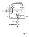
- Fig. 3 shows an embodiment of a current reuse low noise amplifier according to the invention.
- Some bias circuits for example the bias circuit of the second gain stage, are not illustrated for simplicity and clarity.
- This amplifier can be used for amplifying signals in the range of frequencies allowing an integration of the inductances L1 and/or L2 on a silicon slice.
- the frequency of the signal belongs to the range 800 MHz - 6 GHz.
- Each center-tapped differential inductance L1, L2 comprises comprising two magnetically coupled inductances L1' and L1" respectively L2' and L2" with a common center tap.
- the coefficient of coupling between each pair L1'-L1" and L2'-L2" is named K1 respectively K2 in the Figures.
- K1 and K2 are superior to 0.5, preferably 0.7.
- the current reuse low noise amplifier can be used for example and in a non limitative way in a GPS receiver (1.5 GHz) or in a receiver working in the industrial, scientific and medical (ISM) frequency band, for example at 2.4 GHz or 5.8 GHz.
- GPS receiver 1.5 GHz
- ISM industrial, scientific and medical
- the current reuse low noise amplifier of Fig. 3 comprises a first gain stage comprising the transistors M1 and M3, and a second gain stage comprising the transistors M5 to M7.
- the first gain stage comprises a common source transistor M1 and a common gate transistor M3 in a cascode configuration.
- these transistors are NMOS transistors, however they can be also PMOS transistors.
- the second gain stage of. Fig. 3 comprises a cascoded differential pair, i.e. it comprises two branches, the left branch comprising the transistors M5 and M7 in a cascoded configuration, the right branch comprising the transistors M6 and M8 in a cascoded configuration.
- Cascode transistors M7 and M8 are optional and can be inserted for isolation between the input and the output of the second gain stage.
- the first gain stage is connected to the second gain stage by a capacitive coupling and the single-ended to differential signal transformation is performed by the resonant load of the first gain stage operating as a magnetically coupled auto-transformer.
- the resonant load in the illustrated embodiment is the center-tapped differential inductance L1 acting as an auto-transformer with a single-ended input and a differential output.
- L1 comprises two magnetically coupled inductances L1', L1" with a common center tap at Vcom, L1' being connected to the first gain stage, in particular to the transistor M3 and carrying the DC current, L1" generating the 180° phase-shifted differential signal and being an open circuit for DC currents.
- the inductance L1 is designed so that its coefficient of coupling K1 between L1' and L1" is greater than 0.5, preferably greater than 0.6, for example 0.7.
- the harmonics due to amplitude mismatch are strongly suppressed by the filtering effect of the resonance of the inductance L1 with the capacitive load between the two signal ports of the differential inductance L1.
- the same considerations are valid for L2.
- the integrated inductances L1, L2 are designed so as to resonate at the operating frequency due to their own capacitances and to a capacitive load, comprising for example the capacitance of parasitic capacitors to ground.
- the signal is capacitively coupled to the second gain stage by capacitors C1 and C2.
- the single-ended first stage allows a current reduction in the amplifier, while maintaining its performance in terms of the input referred noise: in fact the current that would be required for a differential first stage, illustrated for example in Fig. 1 or 2 , is twice the current required for a single-ended first stage for the same input referred noise performance as illustrated in Fig. 3 . Otherwise the single-ended first stage allows a better performance in term of noise and gain at constant current consumption compared to a differential first stage.
- the single-ended first stage does not limit the linearity of the receiver since the following stages in the receiver chain experience much higher signal amplitudes due to the accumulated voltage gain.
- the single-ended first stage allows also a direct connection to a single-ended antenna, the latter not being included in the figures, furthermore a reduction of the pin count of the integrated circuit comprising this amplifier and the possible reduction of the size of its package.
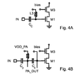
- the first gain stage can comprise one or more inductances L3 for performing an impedance matching, as illustrated in Fig. 4A .
- the LNA has an input impedance which has to be constant and equal to 50 ⁇ within the frequency range of operation, for optimizing the power transmission from the antenna to the low noise amplifier.
- Other impedance value might be required for other antennas.
- the first gain stage comprising the transistors M1 and M3 can be combined with the output of a power amplifier PA_OUT.
- the common source transistor M1 of the first gain stage can be inductively degenerated, in order to obtain the desired impedance matching by using the resonant network formed by the inductances Ls and Lg respectively at the source and at the gate of the transistor M1 and the capacitor Cgs between its source and its gate.
- the desired impedance in such a case is realized in a band of frequency narrower than other solutions.
- the first gain stage comprises a current source I and a common gate transistor M3.
- the transistors of the second gain stage can be PMOS transistors.
- the second gain stage comprises a center-tapped differential inductance L2, formed by two magnetically coupled inductances L2' and L2" as resonant load which is directly above the center-tapped differential inductance L1 of the first gain stage.
- common mode nodes of the resonant networks L1 and L2 of the first and the second amplifier stage can be connected together and biased at roughly half the supply voltage.
- the limitation of supply voltage for a two stage stacked differential amplifier is overcome since the oscillating output signal of the second amplifying stage is generated around a common mode voltage Vcom which is set to roughly half the supply voltage Vsupply of the current reuse low noise amplifier.
- Vcom common mode voltage
- the input to the second gain stage is referred to the supply voltage node while using PMOS transistors M5, M6 as transconductors.
- this arrangement of transistors M5 to M8 allows for an adjustment of the operating point, which assures saturation of all transistors, even at low supply voltages.
- the resonances of both amplifying stages oscillate around the same common mode at about half the supply voltage, thus avoiding technological stress of the output transistors M3, M7 and M8 of the two gain stages.
- a bias circuit not illustrated adjusts the common mode voltage on node Vcom such that the linearity of the two-stage amplifier is optimized.
- the use of two resonances L1 and L2 such that the common mode center taps of the inductances are connected together and biased at about half the supply voltage is not limited to a low noise amplifier having a single-ended input stage, but can be used also in a low noise amplifier having a differential input stage, as illustrated in Fig. 2 .
- the use of a single-ended input stage is not limited to the use of PMOS transistors in the second gain stage, which can be of course composed by NMOS transistors only.
- the second gain stage can be implemented as balanced frequency conversion mixer, which is schematically shown in Figure 5 .
- the mixer function is realised by a Gilbert cell comprising PMOS transistors M9 to M14.
- NMOS transistors and/or other types of mixer can be used as well.
- the described invention allows for example and in a non limitative way to design a LNA for a GPS receiver at 1.5 GHz which consumes 4 mA for a noise figure of 1.5 dB or a LNA for the ISM frequency band (2.4 GHz) which consumes 1.8 mA for a noise figure of 4dB. It is possible also to design a LNA for the ISM frequency band (2.4 GHz) with a current consumption reduced by about 30% compared to the known solutions and a better NF (4 dB instead of 5 dB).
- the given performance values depend of course on factors independent of the present invention, e.g. technological choice (technological node) and options (metallization), external matching, the realizations, etc.
Landscapes
- Engineering & Computer Science (AREA)
- Power Engineering (AREA)
- Amplifiers (AREA)
Priority Applications (1)
| Application Number | Priority Date | Filing Date | Title |
|---|---|---|---|
| EP12176475.7A EP2685630B1 (de) | 2012-07-13 | 2012-07-13 | Zweistufiger rauscharmer Verstärker mit Eintakteingang und Differenzausgangsstromwiederverwendung |
Applications Claiming Priority (1)
| Application Number | Priority Date | Filing Date | Title |
|---|---|---|---|
| EP12176475.7A EP2685630B1 (de) | 2012-07-13 | 2012-07-13 | Zweistufiger rauscharmer Verstärker mit Eintakteingang und Differenzausgangsstromwiederverwendung |
Publications (2)
| Publication Number | Publication Date |
|---|---|
| EP2685630A1 true EP2685630A1 (de) | 2014-01-15 |
| EP2685630B1 EP2685630B1 (de) | 2014-10-22 |
Family
ID=46754273
Family Applications (1)
| Application Number | Title | Priority Date | Filing Date |
|---|---|---|---|
| EP12176475.7A Active EP2685630B1 (de) | 2012-07-13 | 2012-07-13 | Zweistufiger rauscharmer Verstärker mit Eintakteingang und Differenzausgangsstromwiederverwendung |
Country Status (1)
| Country | Link |
|---|---|
| EP (1) | EP2685630B1 (de) |
Cited By (16)
| Publication number | Priority date | Publication date | Assignee | Title |
|---|---|---|---|---|
| US20150091642A1 (en) * | 2013-09-30 | 2015-04-02 | Texas Instruments Incorporated | Method and circuitry for multi-stage amplification |
| CN104539242A (zh) * | 2014-04-21 | 2015-04-22 | 上海华虹宏力半导体制造有限公司 | 电流复用低噪声放大器 |
| CN105391413A (zh) * | 2014-08-28 | 2016-03-09 | 拉碧斯半导体株式会社 | 高频放大电路 |
| WO2016035205A1 (ja) * | 2014-09-05 | 2016-03-10 | 株式会社日立製作所 | 増幅器、それを用いた超音波探触子および診断装置 |
| CN106301242A (zh) * | 2016-09-21 | 2017-01-04 | 无锡中科微电子工业技术研究院有限责任公司 | 电流复用型高频放大器电路 |
| CN109194291A (zh) * | 2018-09-06 | 2019-01-11 | 南京国博电子有限公司 | 一种高增益高线性带旁路功能的单片式低噪声放大器 |
| EP3407084A4 (de) * | 2016-01-22 | 2019-12-11 | Shenzhen Genorivision Technology Co., Ltd. | Ultraschallbildgebungsvorrichtung und -verfahren |
| EP3439176A4 (de) * | 2016-03-31 | 2020-02-12 | Nippon Telegraph and Telephone Corporation | Treiberschaltung und optischer sender |
| CN114124142A (zh) * | 2021-12-01 | 2022-03-01 | 东南大学 | 一种电流复用低功耗差分超再生射频前端电路 |
| WO2022067205A1 (en) * | 2020-09-28 | 2022-03-31 | QuantalRF AG | Amplifier including magnetically coupled feedback loop and stacked input and output stages adapted for dc current reuse |
| CN115694376A (zh) * | 2022-12-29 | 2023-02-03 | 成都嘉纳海威科技有限责任公司 | 一种带连续衰减功能的低功耗放大器 |
| US12052004B2 (en) | 2019-04-02 | 2024-07-30 | QuantaIRF AG | Radio frequency power amplifier system and method of linearizing an output signal thereof |
| CN118646381A (zh) * | 2024-06-17 | 2024-09-13 | 上海芯璨电子科技有限公司 | 射频功率放大器及电子设备 |
| US12149216B2 (en) | 2021-02-09 | 2024-11-19 | QuantalRF AG | System and method for adjusting amplifier bias using envelope tracking |
| US12355428B2 (en) | 2022-08-31 | 2025-07-08 | QuantaIRF AG | System and method for integrated filtering and amplification |
| US12424976B2 (en) | 2021-02-09 | 2025-09-23 | QuantalRF AG | System and method for adjusting amplifier bias current based on input signal envelope tracking |
Citations (4)
| Publication number | Priority date | Publication date | Assignee | Title |
|---|---|---|---|---|
| US20020084855A1 (en) * | 2000-12-28 | 2002-07-04 | Kwon Ick Jin | Low power low noise amplifier |
| US20070176679A1 (en) | 2006-02-01 | 2007-08-02 | Atmel Germany Gmbh | Differential amplifier and radio system with a differential amplifier |
| EP2037572A1 (de) * | 2007-09-17 | 2009-03-18 | Seiko Epson Corporation | Frontend für ein Funksystem mit extrem niedrigem Leistungsverbrauch durch Stromwiederverwendung |
| US20100019848A1 (en) * | 2008-07-28 | 2010-01-28 | Paolo Rossi | Complementary Low Noise Transductor with Active Single Ended to Differential Signal Conversion |
-
2012
- 2012-07-13 EP EP12176475.7A patent/EP2685630B1/de active Active
Patent Citations (5)
| Publication number | Priority date | Publication date | Assignee | Title |
|---|---|---|---|---|
| US20020084855A1 (en) * | 2000-12-28 | 2002-07-04 | Kwon Ick Jin | Low power low noise amplifier |
| US20070176679A1 (en) | 2006-02-01 | 2007-08-02 | Atmel Germany Gmbh | Differential amplifier and radio system with a differential amplifier |
| EP1816742A2 (de) * | 2006-02-01 | 2007-08-08 | ATMEL Germany GmbH | Differenzverstärker und Funksystem mit Differenzverstärker |
| EP2037572A1 (de) * | 2007-09-17 | 2009-03-18 | Seiko Epson Corporation | Frontend für ein Funksystem mit extrem niedrigem Leistungsverbrauch durch Stromwiederverwendung |
| US20100019848A1 (en) * | 2008-07-28 | 2010-01-28 | Paolo Rossi | Complementary Low Noise Transductor with Active Single Ended to Differential Signal Conversion |
Non-Patent Citations (7)
| Title |
|---|
| CHE-HONG LIAO; HUEY-RU CHUANG: "A 5.7 GHz 0.18 pm CMOS Gain-Controlled Differential LNA With Current Reuse for WLAN Receiver", IEEE MICROWAVE AND WIRELESS COMPONENTS LETTERS, vol. 13, no. 12, December 2003 (2003-12-01), XP011106056, DOI: doi:10.1109/LMWC.2003.819379 |
| GRAMEGNA G ET AL: "An 8.2-ghz, 14.4mw, 1.6db nf sige bipolar lna with dc current reuse", PROCEEDINGS OF THE 2003 BIPOLAR/BICMOS CIRCUITS AND TECHNOLOGY MEETING. ( BCTM ). TOULOUSE, FRANCE, SEPT. 28 - 30, 2003; [IEEE BIPOLAR/BICMOS CIRCUITS AND TECHNOLOGY MEETING], NEW YORK, NY : IEEE, US, 28 September 2003 (2003-09-28), pages 49 - 52, XP010688453, ISBN: 978-0-7803-7800-1, DOI: 10.1109/BIPOL.2003.1274933 * |
| HSIEH-HUNG HSIEH ET AL: "Design of Ultra-Low-Voltage RF Frontends With Complementary Current-Reused Architectures", IEEE TRANSACTIONS ON MICROWAVE THEORY AND TECHNIQUES, IEEE SERVICE CENTER, PISCATAWAY, NJ, US, vol. 49, no. 7, 1 July 2007 (2007-07-01), pages 1445 - 1458, XP011187189, ISSN: 0018-9480, DOI: 10.1109/TMTT.2007.900208 * |
| INUI C ET AL: "60GHz CMOS Current-Reuse Cascade Amplifier", MICROWAVE CONFERENCE, 2007. APMC 2007. ASIA-PACIFIC, IEEE, PISCATAWAY, NJ, USA, 11 December 2007 (2007-12-11), pages 1 - 4, XP031280103, ISBN: 978-1-4244-0748-4 * |
| PENG WANG ET AL: "A novel low-power fully-differential current-reuse cascaded CG-CS-LNA for 6â 9-GHz UWB receivers", ELECTRONICS, CIRCUITS, AND SYSTEMS (ICECS), 2010 17TH IEEE INTERNATIONAL CONFERENCE ON, IEEE, 12 December 2010 (2010-12-12), pages 1188 - 1191, XP031923168, ISBN: 978-1-4244-8155-2, DOI: 10.1109/ICECS.2010.5724730 * |
| SIROOS TOOFAN ET AL: "A 5.5-GHz 3mW LNA and inductive degenerative CMOS LNA noise figure calculation", MICROELECTRONICS, 2008. ICM 2008. INTERNATIONAL CONFERENCE ON, IEEE, PISCATAWAY, NJ, USA, 14 December 2008 (2008-12-14), pages 308 - 312, XP031615487, ISBN: 978-1-4244-2369-9 * |
| VITTORIO GIAMMELLO ET AL: "A Transformer-Coupling Current-Reuse SiGe HBT Power Amplifier for 77-GHz Automotive Radar", IEEE TRANSACTIONS ON MICROWAVE THEORY AND TECHNIQUES, IEEE SERVICE CENTER, PISCATAWAY, NJ, US, vol. 60, no. 6, 1 June 2012 (2012-06-01), pages 1676 - 1683, XP011445272, ISSN: 0018-9480, DOI: 10.1109/TMTT.2012.2189243 * |
Cited By (28)
| Publication number | Priority date | Publication date | Assignee | Title |
|---|---|---|---|---|
| US9143100B2 (en) * | 2013-09-30 | 2015-09-22 | Texas Instruments Incorporated | Method and circuitry for multi-stage amplification |
| US20150091642A1 (en) * | 2013-09-30 | 2015-04-02 | Texas Instruments Incorporated | Method and circuitry for multi-stage amplification |
| CN104539242B (zh) * | 2014-04-21 | 2019-01-04 | 上海华虹宏力半导体制造有限公司 | 电流复用低噪声放大器 |
| CN104539242A (zh) * | 2014-04-21 | 2015-04-22 | 上海华虹宏力半导体制造有限公司 | 电流复用低噪声放大器 |
| CN105391413B (zh) * | 2014-08-28 | 2019-10-22 | 拉碧斯半导体株式会社 | 高频放大电路 |
| JP2016051906A (ja) * | 2014-08-28 | 2016-04-11 | ラピスセミコンダクタ株式会社 | 高周波増幅回路 |
| CN105391413A (zh) * | 2014-08-28 | 2016-03-09 | 拉碧斯半导体株式会社 | 高频放大电路 |
| WO2016035205A1 (ja) * | 2014-09-05 | 2016-03-10 | 株式会社日立製作所 | 増幅器、それを用いた超音波探触子および診断装置 |
| EP3407084A4 (de) * | 2016-01-22 | 2019-12-11 | Shenzhen Genorivision Technology Co., Ltd. | Ultraschallbildgebungsvorrichtung und -verfahren |
| EP3439176A4 (de) * | 2016-03-31 | 2020-02-12 | Nippon Telegraph and Telephone Corporation | Treiberschaltung und optischer sender |
| US10666212B2 (en) | 2016-03-31 | 2020-05-26 | Nippon Telegraph And Telephone Corporation | Driver circuit and optical transmitter |
| CN106301242A (zh) * | 2016-09-21 | 2017-01-04 | 无锡中科微电子工业技术研究院有限责任公司 | 电流复用型高频放大器电路 |
| CN109194291A (zh) * | 2018-09-06 | 2019-01-11 | 南京国博电子有限公司 | 一种高增益高线性带旁路功能的单片式低噪声放大器 |
| US12052004B2 (en) | 2019-04-02 | 2024-07-30 | QuantaIRF AG | Radio frequency power amplifier system and method of linearizing an output signal thereof |
| WO2022067205A1 (en) * | 2020-09-28 | 2022-03-31 | QuantalRF AG | Amplifier including magnetically coupled feedback loop and stacked input and output stages adapted for dc current reuse |
| US12160203B2 (en) | 2020-09-28 | 2024-12-03 | QuantalRF AG | Amplifier linearization using magnetically coupled feedback provided by a transformer coupled to a balun-based load |
| US11979114B2 (en) | 2020-09-28 | 2024-05-07 | QuantalRF AG | Amplifier including magnetically coupled feedback loop and stacked input and output stages adapted for DC current reuse |
| US12034411B2 (en) | 2020-09-28 | 2024-07-09 | QuantalRF AG | Method of improving linearity of amplifier circuit including magnetically coupled feedback loop and DC bias current adjustment without impacting amplifier gain |
| US12278599B2 (en) | 2020-09-28 | 2025-04-15 | QuantalRF AG | Differential amplifier including dual magnetically coupled feedback loops |
| US12149210B2 (en) | 2020-09-28 | 2024-11-19 | QuantalRF AG | Amplifier linearization using magnetically coupled feedback |
| US12424976B2 (en) | 2021-02-09 | 2025-09-23 | QuantalRF AG | System and method for adjusting amplifier bias current based on input signal envelope tracking |
| US12149216B2 (en) | 2021-02-09 | 2024-11-19 | QuantalRF AG | System and method for adjusting amplifier bias using envelope tracking |
| CN114124142A (zh) * | 2021-12-01 | 2022-03-01 | 东南大学 | 一种电流复用低功耗差分超再生射频前端电路 |
| US12355428B2 (en) | 2022-08-31 | 2025-07-08 | QuantaIRF AG | System and method for integrated filtering and amplification |
| US12519456B2 (en) | 2022-08-31 | 2026-01-06 | QuantalRF AG | Integrated coupled resonator filtering |
| US12567855B2 (en) | 2022-08-31 | 2026-03-03 | QuantalRF AG | System and method for coupled resonator filtering |
| CN115694376A (zh) * | 2022-12-29 | 2023-02-03 | 成都嘉纳海威科技有限责任公司 | 一种带连续衰减功能的低功耗放大器 |
| CN118646381A (zh) * | 2024-06-17 | 2024-09-13 | 上海芯璨电子科技有限公司 | 射频功率放大器及电子设备 |
Also Published As
| Publication number | Publication date |
|---|---|
| EP2685630B1 (de) | 2014-10-22 |
Similar Documents
| Publication | Publication Date | Title |
|---|---|---|
| EP2685630B1 (de) | Zweistufiger rauscharmer Verstärker mit Eintakteingang und Differenzausgangsstromwiederverwendung | |
| CN113783538B (zh) | 一种cmos低噪声放大器 | |
| JP6386312B2 (ja) | 半導体装置 | |
| US7768350B2 (en) | Output gain stage for a power amplifier | |
| EP2854288B1 (de) | Anpassungsnetzwerk zur Verwendung mit einem Verstärker | |
| US8324973B2 (en) | Low output impedance RF amplifier | |
| CN106063125B (zh) | 低噪声放大器电路 | |
| CN102946230B (zh) | 一种超宽带单端输入差分输出低噪声放大器 | |
| KR101126052B1 (ko) | 저잡음 및 저입력 커패시턴스 차동 mds lna | |
| US10305533B2 (en) | Semiconductor device | |
| US7804361B2 (en) | Low noise amplifier | |
| KR101125500B1 (ko) | 사후-왜곡 모드 및 고이득 모드를 갖는 lna | |
| CN102340288B (zh) | 一种具有阻抗匹配的射频集成带通滤波器 | |
| CN111434031A (zh) | 功率放大器电路 | |
| JP2010537453A (ja) | チューナブルインピーダンス整合回路 | |
| CN103532503A (zh) | 功率放大器 | |
| WO2006116527A1 (en) | Differential inductor based low noise amplifier | |
| JP2009005137A (ja) | 高周波回路 | |
| Aneja et al. | Multiband LNAs for software-defined radios: recent advances in the design of multiband reconfigurable LNAs for SDRs in CMOS, microwave integrated circuits technology | |
| US20260058617A1 (en) | Low noise amplifier incorporating sutardja transformer | |
| CN119787991B (zh) | 应用于毫米波的低噪声放大器 | |
| CN103095222A (zh) | 一种带有失配补偿技术的有源Balun | |
| KR101135190B1 (ko) | 발룬 회로를 이용한 무선 통신 시스템의 신호 변환 장치 및 수신 장치 | |
| US10771023B2 (en) | Amplifier | |
| Liu et al. | A 26-38GHz Ultra-Wideband Balanced Frequency Doubler in 0.15 µ m GaAs pHEMT Process |
Legal Events
| Date | Code | Title | Description |
|---|---|---|---|
| PUAI | Public reference made under article 153(3) epc to a published international application that has entered the european phase |
Free format text: ORIGINAL CODE: 0009012 |
|
| AK | Designated contracting states |
Kind code of ref document: A1 Designated state(s): AL AT BE BG CH CY CZ DE DK EE ES FI FR GB GR HR HU IE IS IT LI LT LU LV MC MK MT NL NO PL PT RO RS SE SI SK SM TR |
|
| AX | Request for extension of the european patent |
Extension state: BA ME |
|
| 17P | Request for examination filed |
Effective date: 20140331 |
|
| RBV | Designated contracting states (corrected) |
Designated state(s): AL AT BE BG CH CY CZ DE DK EE ES FI FR GB GR HR HU IE IS IT LI LT LU LV MC MK MT NL NO PL PT RO RS SE SI SK SM TR |
|
| GRAP | Despatch of communication of intention to grant a patent |
Free format text: ORIGINAL CODE: EPIDOSNIGR1 |
|
| INTG | Intention to grant announced |
Effective date: 20140605 |
|
| GRAS | Grant fee paid |
Free format text: ORIGINAL CODE: EPIDOSNIGR3 |
|
| GRAA | (expected) grant |
Free format text: ORIGINAL CODE: 0009210 |
|
| AK | Designated contracting states |
Kind code of ref document: B1 Designated state(s): AL AT BE BG CH CY CZ DE DK EE ES FI FR GB GR HR HU IE IS IT LI LT LU LV MC MK MT NL NO PL PT RO RS SE SI SK SM TR |
|
| REG | Reference to a national code |
Ref country code: GB Ref legal event code: FG4D |
|
| REG | Reference to a national code |
Ref country code: CH Ref legal event code: EP |
|
| REG | Reference to a national code |
Ref country code: CH Ref legal event code: NV Representative=s name: P&TS SA, CH |
|
| REG | Reference to a national code |
Ref country code: AT Ref legal event code: REF Ref document number: 693027 Country of ref document: AT Kind code of ref document: T Effective date: 20141115 |
|
| REG | Reference to a national code |
Ref country code: IE Ref legal event code: FG4D |
|
| REG | Reference to a national code |
Ref country code: DE Ref legal event code: R096 Ref document number: 602012003473 Country of ref document: DE Effective date: 20141204 |
|
| REG | Reference to a national code |
Ref country code: NL Ref legal event code: VDEP Effective date: 20141022 |
|
| REG | Reference to a national code |
Ref country code: AT Ref legal event code: MK05 Ref document number: 693027 Country of ref document: AT Kind code of ref document: T Effective date: 20141022 |
|
| REG | Reference to a national code |
Ref country code: LT Ref legal event code: MG4D |
|
| PG25 | Lapsed in a contracting state [announced via postgrant information from national office to epo] |
Ref country code: FI Free format text: LAPSE BECAUSE OF FAILURE TO SUBMIT A TRANSLATION OF THE DESCRIPTION OR TO PAY THE FEE WITHIN THE PRESCRIBED TIME-LIMIT Effective date: 20141022 Ref country code: NL Free format text: LAPSE BECAUSE OF FAILURE TO SUBMIT A TRANSLATION OF THE DESCRIPTION OR TO PAY THE FEE WITHIN THE PRESCRIBED TIME-LIMIT Effective date: 20141022 Ref country code: PT Free format text: LAPSE BECAUSE OF FAILURE TO SUBMIT A TRANSLATION OF THE DESCRIPTION OR TO PAY THE FEE WITHIN THE PRESCRIBED TIME-LIMIT Effective date: 20150223 Ref country code: NO Free format text: LAPSE BECAUSE OF FAILURE TO SUBMIT A TRANSLATION OF THE DESCRIPTION OR TO PAY THE FEE WITHIN THE PRESCRIBED TIME-LIMIT Effective date: 20150122 Ref country code: IS Free format text: LAPSE BECAUSE OF FAILURE TO SUBMIT A TRANSLATION OF THE DESCRIPTION OR TO PAY THE FEE WITHIN THE PRESCRIBED TIME-LIMIT Effective date: 20150222 Ref country code: ES Free format text: LAPSE BECAUSE OF FAILURE TO SUBMIT A TRANSLATION OF THE DESCRIPTION OR TO PAY THE FEE WITHIN THE PRESCRIBED TIME-LIMIT Effective date: 20141022 Ref country code: LT Free format text: LAPSE BECAUSE OF FAILURE TO SUBMIT A TRANSLATION OF THE DESCRIPTION OR TO PAY THE FEE WITHIN THE PRESCRIBED TIME-LIMIT Effective date: 20141022 |
|
| PG25 | Lapsed in a contracting state [announced via postgrant information from national office to epo] |
Ref country code: LV Free format text: LAPSE BECAUSE OF FAILURE TO SUBMIT A TRANSLATION OF THE DESCRIPTION OR TO PAY THE FEE WITHIN THE PRESCRIBED TIME-LIMIT Effective date: 20141022 Ref country code: GR Free format text: LAPSE BECAUSE OF FAILURE TO SUBMIT A TRANSLATION OF THE DESCRIPTION OR TO PAY THE FEE WITHIN THE PRESCRIBED TIME-LIMIT Effective date: 20150123 Ref country code: CY Free format text: LAPSE BECAUSE OF FAILURE TO SUBMIT A TRANSLATION OF THE DESCRIPTION OR TO PAY THE FEE WITHIN THE PRESCRIBED TIME-LIMIT Effective date: 20141022 Ref country code: RS Free format text: LAPSE BECAUSE OF FAILURE TO SUBMIT A TRANSLATION OF THE DESCRIPTION OR TO PAY THE FEE WITHIN THE PRESCRIBED TIME-LIMIT Effective date: 20141022 Ref country code: SE Free format text: LAPSE BECAUSE OF FAILURE TO SUBMIT A TRANSLATION OF THE DESCRIPTION OR TO PAY THE FEE WITHIN THE PRESCRIBED TIME-LIMIT Effective date: 20141022 Ref country code: HR Free format text: LAPSE BECAUSE OF FAILURE TO SUBMIT A TRANSLATION OF THE DESCRIPTION OR TO PAY THE FEE WITHIN THE PRESCRIBED TIME-LIMIT Effective date: 20141022 Ref country code: AT Free format text: LAPSE BECAUSE OF FAILURE TO SUBMIT A TRANSLATION OF THE DESCRIPTION OR TO PAY THE FEE WITHIN THE PRESCRIBED TIME-LIMIT Effective date: 20141022 Ref country code: PL Free format text: LAPSE BECAUSE OF FAILURE TO SUBMIT A TRANSLATION OF THE DESCRIPTION OR TO PAY THE FEE WITHIN THE PRESCRIBED TIME-LIMIT Effective date: 20141022 |
|
| REG | Reference to a national code |
Ref country code: DE Ref legal event code: R097 Ref document number: 602012003473 Country of ref document: DE |
|
| PG25 | Lapsed in a contracting state [announced via postgrant information from national office to epo] |
Ref country code: EE Free format text: LAPSE BECAUSE OF FAILURE TO SUBMIT A TRANSLATION OF THE DESCRIPTION OR TO PAY THE FEE WITHIN THE PRESCRIBED TIME-LIMIT Effective date: 20141022 Ref country code: CZ Free format text: LAPSE BECAUSE OF FAILURE TO SUBMIT A TRANSLATION OF THE DESCRIPTION OR TO PAY THE FEE WITHIN THE PRESCRIBED TIME-LIMIT Effective date: 20141022 Ref country code: SK Free format text: LAPSE BECAUSE OF FAILURE TO SUBMIT A TRANSLATION OF THE DESCRIPTION OR TO PAY THE FEE WITHIN THE PRESCRIBED TIME-LIMIT Effective date: 20141022 Ref country code: RO Free format text: LAPSE BECAUSE OF FAILURE TO SUBMIT A TRANSLATION OF THE DESCRIPTION OR TO PAY THE FEE WITHIN THE PRESCRIBED TIME-LIMIT Effective date: 20141022 Ref country code: DK Free format text: LAPSE BECAUSE OF FAILURE TO SUBMIT A TRANSLATION OF THE DESCRIPTION OR TO PAY THE FEE WITHIN THE PRESCRIBED TIME-LIMIT Effective date: 20141022 |
|
| REG | Reference to a national code |
Ref country code: FR Ref legal event code: PLFP Year of fee payment: 4 |
|
| PLBE | No opposition filed within time limit |
Free format text: ORIGINAL CODE: 0009261 |
|
| STAA | Information on the status of an ep patent application or granted ep patent |
Free format text: STATUS: NO OPPOSITION FILED WITHIN TIME LIMIT |
|
| PG25 | Lapsed in a contracting state [announced via postgrant information from national office to epo] |
Ref country code: IT Free format text: LAPSE BECAUSE OF FAILURE TO SUBMIT A TRANSLATION OF THE DESCRIPTION OR TO PAY THE FEE WITHIN THE PRESCRIBED TIME-LIMIT Effective date: 20141022 |
|
| 26N | No opposition filed |
Effective date: 20150723 |
|
| PG25 | Lapsed in a contracting state [announced via postgrant information from national office to epo] |
Ref country code: MC Free format text: LAPSE BECAUSE OF FAILURE TO SUBMIT A TRANSLATION OF THE DESCRIPTION OR TO PAY THE FEE WITHIN THE PRESCRIBED TIME-LIMIT Effective date: 20141022 Ref country code: SI Free format text: LAPSE BECAUSE OF FAILURE TO SUBMIT A TRANSLATION OF THE DESCRIPTION OR TO PAY THE FEE WITHIN THE PRESCRIBED TIME-LIMIT Effective date: 20141022 |
|
| PG25 | Lapsed in a contracting state [announced via postgrant information from national office to epo] |
Ref country code: LU Free format text: LAPSE BECAUSE OF FAILURE TO SUBMIT A TRANSLATION OF THE DESCRIPTION OR TO PAY THE FEE WITHIN THE PRESCRIBED TIME-LIMIT Effective date: 20150713 |
|
| REG | Reference to a national code |
Ref country code: IE Ref legal event code: MM4A |
|
| REG | Reference to a national code |
Ref country code: FR Ref legal event code: PLFP Year of fee payment: 5 |
|
| PG25 | Lapsed in a contracting state [announced via postgrant information from national office to epo] |
Ref country code: IE Free format text: LAPSE BECAUSE OF NON-PAYMENT OF DUE FEES Effective date: 20150713 |
|
| PG25 | Lapsed in a contracting state [announced via postgrant information from national office to epo] |
Ref country code: MT Free format text: LAPSE BECAUSE OF FAILURE TO SUBMIT A TRANSLATION OF THE DESCRIPTION OR TO PAY THE FEE WITHIN THE PRESCRIBED TIME-LIMIT Effective date: 20141022 |
|
| PG25 | Lapsed in a contracting state [announced via postgrant information from national office to epo] |
Ref country code: SM Free format text: LAPSE BECAUSE OF FAILURE TO SUBMIT A TRANSLATION OF THE DESCRIPTION OR TO PAY THE FEE WITHIN THE PRESCRIBED TIME-LIMIT Effective date: 20141022 Ref country code: HU Free format text: LAPSE BECAUSE OF FAILURE TO SUBMIT A TRANSLATION OF THE DESCRIPTION OR TO PAY THE FEE WITHIN THE PRESCRIBED TIME-LIMIT; INVALID AB INITIO Effective date: 20120713 Ref country code: BG Free format text: LAPSE BECAUSE OF FAILURE TO SUBMIT A TRANSLATION OF THE DESCRIPTION OR TO PAY THE FEE WITHIN THE PRESCRIBED TIME-LIMIT Effective date: 20141022 |
|
| REG | Reference to a national code |
Ref country code: FR Ref legal event code: PLFP Year of fee payment: 6 |
|
| PG25 | Lapsed in a contracting state [announced via postgrant information from national office to epo] |
Ref country code: BE Free format text: LAPSE BECAUSE OF FAILURE TO SUBMIT A TRANSLATION OF THE DESCRIPTION OR TO PAY THE FEE WITHIN THE PRESCRIBED TIME-LIMIT Effective date: 20141022 |
|
| PG25 | Lapsed in a contracting state [announced via postgrant information from national office to epo] |
Ref country code: MK Free format text: LAPSE BECAUSE OF FAILURE TO SUBMIT A TRANSLATION OF THE DESCRIPTION OR TO PAY THE FEE WITHIN THE PRESCRIBED TIME-LIMIT Effective date: 20141022 Ref country code: TR Free format text: LAPSE BECAUSE OF FAILURE TO SUBMIT A TRANSLATION OF THE DESCRIPTION OR TO PAY THE FEE WITHIN THE PRESCRIBED TIME-LIMIT Effective date: 20141022 |
|
| REG | Reference to a national code |
Ref country code: FR Ref legal event code: PLFP Year of fee payment: 7 |
|
| PG25 | Lapsed in a contracting state [announced via postgrant information from national office to epo] |
Ref country code: AL Free format text: LAPSE BECAUSE OF FAILURE TO SUBMIT A TRANSLATION OF THE DESCRIPTION OR TO PAY THE FEE WITHIN THE PRESCRIBED TIME-LIMIT Effective date: 20141022 |
|
| PGFP | Annual fee paid to national office [announced via postgrant information from national office to epo] |
Ref country code: DE Payment date: 20250722 Year of fee payment: 14 |
|
| PGFP | Annual fee paid to national office [announced via postgrant information from national office to epo] |
Ref country code: GB Payment date: 20250724 Year of fee payment: 14 |
|
| PGFP | Annual fee paid to national office [announced via postgrant information from national office to epo] |
Ref country code: FR Payment date: 20250723 Year of fee payment: 14 |
|
| PGFP | Annual fee paid to national office [announced via postgrant information from national office to epo] |
Ref country code: CH Payment date: 20250801 Year of fee payment: 14 |
|
| REG | Reference to a national code |
Ref country code: CH Ref legal event code: U11 Free format text: ST27 STATUS EVENT CODE: U-0-0-U10-U11 (AS PROVIDED BY THE NATIONAL OFFICE) Effective date: 20260801 |