EP2685802A2 - Absorber elektromagnetischer Wellen - Google Patents
Absorber elektromagnetischer Wellen Download PDFInfo
- Publication number
- EP2685802A2 EP2685802A2 EP20130175682 EP13175682A EP2685802A2 EP 2685802 A2 EP2685802 A2 EP 2685802A2 EP 20130175682 EP20130175682 EP 20130175682 EP 13175682 A EP13175682 A EP 13175682A EP 2685802 A2 EP2685802 A2 EP 2685802A2
- Authority
- EP
- European Patent Office
- Prior art keywords
- shaped part
- plate
- oblong rectangular
- pyramidal
- wave absorber
- Prior art date
- Legal status (The legal status is an assumption and is not a legal conclusion. Google has not performed a legal analysis and makes no representation as to the accuracy of the status listed.)
- Withdrawn
Links
- 239000006096 absorbing agent Substances 0.000 title claims abstract description 67
- 239000000463 material Substances 0.000 description 18
- OKTJSMMVPCPJKN-UHFFFAOYSA-N Carbon Chemical compound [C] OKTJSMMVPCPJKN-UHFFFAOYSA-N 0.000 description 16
- 230000005670 electromagnetic radiation Effects 0.000 description 16
- 229910000859 α-Fe Inorganic materials 0.000 description 15
- 238000010521 absorption reaction Methods 0.000 description 14
- 229910052799 carbon Inorganic materials 0.000 description 8
- 239000004568 cement Substances 0.000 description 8
- 239000002041 carbon nanotube Substances 0.000 description 7
- 229910021393 carbon nanotube Inorganic materials 0.000 description 7
- VYPSYNLAJGMNEJ-UHFFFAOYSA-N Silicium dioxide Chemical compound O=[Si]=O VYPSYNLAJGMNEJ-UHFFFAOYSA-N 0.000 description 6
- MCMNRKCIXSYSNV-UHFFFAOYSA-N Zirconium dioxide Chemical compound O=[Zr]=O MCMNRKCIXSYSNV-UHFFFAOYSA-N 0.000 description 6
- 230000000052 comparative effect Effects 0.000 description 5
- 238000000034 method Methods 0.000 description 5
- 239000000843 powder Substances 0.000 description 5
- 239000011347 resin Substances 0.000 description 5
- 229920005989 resin Polymers 0.000 description 5
- 239000011358 absorbing material Substances 0.000 description 4
- 229910010272 inorganic material Inorganic materials 0.000 description 4
- 239000011147 inorganic material Substances 0.000 description 4
- 230000005855 radiation Effects 0.000 description 4
- 239000002002 slurry Substances 0.000 description 4
- PNEYBMLMFCGWSK-UHFFFAOYSA-N aluminium oxide Inorganic materials [O-2].[O-2].[O-2].[Al+3].[Al+3] PNEYBMLMFCGWSK-UHFFFAOYSA-N 0.000 description 3
- 238000004891 communication Methods 0.000 description 3
- 239000000377 silicon dioxide Substances 0.000 description 3
- XLYOFNOQVPJJNP-UHFFFAOYSA-N water Substances O XLYOFNOQVPJJNP-UHFFFAOYSA-N 0.000 description 3
- 239000004743 Polypropylene Substances 0.000 description 2
- 238000010276 construction Methods 0.000 description 2
- 238000011156 evaluation Methods 0.000 description 2
- 238000005259 measurement Methods 0.000 description 2
- -1 polypropylene Polymers 0.000 description 2
- 229920001155 polypropylene Polymers 0.000 description 2
- 229920002635 polyurethane Polymers 0.000 description 2
- 239000004814 polyurethane Substances 0.000 description 2
- 238000005245 sintering Methods 0.000 description 2
- 239000007787 solid Substances 0.000 description 2
- 229910008405 Li-Zn Inorganic materials 0.000 description 1
- 229910007049 Li—Zn Inorganic materials 0.000 description 1
- 229910018605 Ni—Zn Inorganic materials 0.000 description 1
- 239000004793 Polystyrene Substances 0.000 description 1
- 239000011398 Portland cement Substances 0.000 description 1
- 239000003990 capacitor Substances 0.000 description 1
- 239000006229 carbon black Substances 0.000 description 1
- 239000003575 carbonaceous material Substances 0.000 description 1
- 238000005266 casting Methods 0.000 description 1
- 229910010293 ceramic material Inorganic materials 0.000 description 1
- 238000002485 combustion reaction Methods 0.000 description 1
- 239000004020 conductor Substances 0.000 description 1
- 238000011161 development Methods 0.000 description 1
- 239000002270 dispersing agent Substances 0.000 description 1
- 230000001747 exhibiting effect Effects 0.000 description 1
- 229920006248 expandable polystyrene Polymers 0.000 description 1
- 229910002804 graphite Inorganic materials 0.000 description 1
- 239000010439 graphite Substances 0.000 description 1
- 238000011835 investigation Methods 0.000 description 1
- 150000002500 ions Chemical class 0.000 description 1
- 238000004898 kneading Methods 0.000 description 1
- 230000007257 malfunction Effects 0.000 description 1
- 239000011159 matrix material Substances 0.000 description 1
- 238000002156 mixing Methods 0.000 description 1
- 238000000465 moulding Methods 0.000 description 1
- 229920002223 polystyrene Polymers 0.000 description 1
- 239000006100 radiation absorber Substances 0.000 description 1
- 239000002994 raw material Substances 0.000 description 1
- 239000012260 resinous material Substances 0.000 description 1
- 229910052596 spinel Inorganic materials 0.000 description 1
- 239000011029 spinel Substances 0.000 description 1
- 238000003756 stirring Methods 0.000 description 1
- 239000000057 synthetic resin Substances 0.000 description 1
- 229920003002 synthetic resin Polymers 0.000 description 1
Images
Classifications
-
- H—ELECTRICITY
- H05—ELECTRIC TECHNIQUES NOT OTHERWISE PROVIDED FOR
- H05K—PRINTED CIRCUITS; CASINGS OR CONSTRUCTIONAL DETAILS OF ELECTRIC APPARATUS; MANUFACTURE OF ASSEMBLAGES OF ELECTRICAL COMPONENTS
- H05K9/00—Screening of apparatus or components against electric or magnetic fields
-
- H—ELECTRICITY
- H01—ELECTRIC ELEMENTS
- H01Q—ANTENNAS, i.e. RADIO AERIALS
- H01Q17/00—Devices for absorbing waves radiated from an antenna; Combinations of such devices with active antenna elements or systems
- H01Q17/008—Devices for absorbing waves radiated from an antenna; Combinations of such devices with active antenna elements or systems with a particular shape
-
- H—ELECTRICITY
- H01—ELECTRIC ELEMENTS
- H01Q—ANTENNAS, i.e. RADIO AERIALS
- H01Q17/00—Devices for absorbing waves radiated from an antenna; Combinations of such devices with active antenna elements or systems
- H01Q17/002—Devices for absorbing waves radiated from an antenna; Combinations of such devices with active antenna elements or systems using short elongated elements as dissipative material, e.g. metallic threads or flake-like particles
-
- H—ELECTRICITY
- H05—ELECTRIC TECHNIQUES NOT OTHERWISE PROVIDED FOR
- H05K—PRINTED CIRCUITS; CASINGS OR CONSTRUCTIONAL DETAILS OF ELECTRIC APPARATUS; MANUFACTURE OF ASSEMBLAGES OF ELECTRICAL COMPONENTS
- H05K9/00—Screening of apparatus or components against electric or magnetic fields
- H05K9/0007—Casings
- H05K9/0052—Shielding other than Faraday cages
Definitions
- This invention relates to an electromagnetic wave absorber, more particularly a small-sized electromagnetic wave absorber having excellent absorbing performance for oblique incident angles as well as normal.
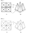
- Electromagnetic radiation absorbers (hereinafter referred to as wave absorber (s) or simply absorber (s)) conventionally used in anechoic chambers are integrally molded structures having, as illustrated in Fig. 1 , a plate-shaped part 1 and a polygonal pyramidal or wedge-shaped parts 2.
- These wave absorbers are dielectric loss structures made by expansion-molding an electromagnetic radiation absorbing material comprising a synthetic resin, such as polyurethane, polystyrene, or polypropylene, and an electrically conductive material, such as carbon.
- a hybrid wave absorber composed of a ferrite tile and the wave absorber of the dielectric loss type placed on the ferrite tile is known to exhibit good radiation absorption characteristics even with a reduced height of the dielectric loss structure because electromagnetic waves in a high frequency range of 100 MHz or higher are absorbed by the dielectric structure while electromagnetic waves in a low frequency range are absorbed by the ferrite tile, i.e., a magnetic absorber.
- this hybrid wave absorber there is provided an anechoic chamber of smaller size.
- JP 2000-188513A discloses a wave absorber composed of a ferrite tile and an upper absorber having a wedge or pyramidal shape, the upper absorber being a molded part comprising a general purpose type resin having a relative permittivity of 4.9 or less at a frequency of 1MHz or higher and ferrite powder dispersed in the resin.
- the wave absorber is described as being capable of absorbing higher frequency waves with the height of the upper absorber being equal to that of conventional wave absorbers.
- JP 2000-188513A also discloses a panel having four pyramidal parts the bottom of which are integrally connected to each other, the panel having a portion for screwing (e.g., a through-hole) at the center and on each of the four side edges thereof so that the absorber may be firmly fixed to construct an anechoic chamber with ease.
- a portion for screwing e.g., a through-hole
- JP 2000-188513A shows excellent absorption characteristics for normal incidence of electromagnetic radiation.
- electromagnetic waves are incident on the ceiling and side walls of an anechoic chamber at a certain angle.
- the angle of incidence is about 40° in a 10 m anechoic chamber.
- a wave absorber having absorption performance for oblique incidence as well as normal is required.
- the pyramidal shape of the absorber described in JP 2000-188513A has all the faces at the same angle of inclination, which is designed with weight put on normal incidence without due considerations given to oblique incidence characteristics.
- adjacent pyramidal parts 2 In order to provide the structure of JP 2000-188513A with through-holes for screwing, adjacent pyramidal parts 2 must be arranged on the plate-shaped part 1 at a predetermined space, and a flat portion should be provided at the center of the panel as shown in Fig. 1 .
- Such an arrangement of wave absorbers involves reduction of absorbing performance due to reflection on these flat portions, and the reduction of absorbing performance should be compensated for by, for example, increasing the height of the pyramidal parts 2.
- An object of the invention is to provide an electromagnetic wave absorber excellent in absorption characteristics for oblique incidence as well as normal and suited for designing a small-sized and high-performance anechoic chamber.
- An electromagnetic wave absorber comprising a rectangular plate-shaped part having a surface comprising a flat space at a center of the plate-shaped part and a plurality of oblong rectangular spaces, surrounding the flat space, on each of which at least one pyramidal or wedge-shaped part having an oblong rectangular bottom face is provided, wherein the plurality of oblong rectangular spaces of the surface of the plate-shaped part are arranged along inside a perimeter of the plate-shaped part so that a longer side of any one of the plurality of oblong rectangular spaces is adjoining with a shorter side of another of the plurality of oblong rectangular spaces adjacent thereto while leaving the flat space at the center of the plate-shaped part.
- a wave absorber that is small and yet exhibits not only excellent normal incidence characteristics but also improved oblique incidence characteristics is obtained by arranging, on a rectangular plate-shaped part, a plurality of (e.g., four) oblong rectangular pyramidal or wedge-shaped parts along inside the perimeter of the plate-shaped part with a longer side of the rectangular bottom face of one pyramidal or wedge-shaped part adjoining with a shorter side of the rectangular bottom face of an adjacent pyramidal or wedge-shaped part while leaving a flat space at the center of the plate-shaped part.
- a plurality of (e.g., four) oblong rectangular pyramidal or wedge-shaped parts along inside the perimeter of the plate-shaped part with a longer side of the rectangular bottom face of one pyramidal or wedge-shaped part adjoining with a shorter side of the rectangular bottom face of an adjacent pyramidal or wedge-shaped part while leaving a flat space at the center of the plate-shaped part.
- the preferable embodiment of the invention thus provides a wave absorber comprising a rectangular plate-shaped part and a plurality of (e.g., four) oblong rectangular pyramidal or wedge-shaped parts along inside the perimeter of the plate-shaped part with a longer side of the oblong rectangular bottom face of one pyramidal or wedge-shaped part adjoining with a shorter side of the oblong rectangular bottom face of an adjacent pyramidal or wedge-shaped part while leaving a flat space at the center of the plate-shaped part.
- a wave absorber comprising a rectangular plate-shaped part and a plurality of (e.g., four) oblong rectangular pyramidal or wedge-shaped parts along inside the perimeter of the plate-shaped part with a longer side of the oblong rectangular bottom face of one pyramidal or wedge-shaped part adjoining with a shorter side of the oblong rectangular bottom face of an adjacent pyramidal or wedge-shaped part while leaving a flat space at the center of the plate-shaped part.
- the wave absorber of the invention has a geometry in which a plurality of oblong rectangular spaces (a plurality of oblong rectangular pyramidal or wedge-shaped parts in case of the preferable embodiment) are arranged with a longer side of one oblong rectangular space (a longer side of the oblong rectangular bottom face of one pyramidal or wedge-shaped part in case of the preferable embodiment) adjoining with a shorter side of an adjacent oblong rectangular space (a shorter side of the oblong rectangular bottom face of an adjacent pyramidal or wedge-shaped part in case of the preferable embodiment) while leaving a flat space at the center of the plate-shaped part.
- the wave absorber achieves excellent wave absorbing performance even with a reduced size. Ease of constructing an anechoic chamber is maintained with this geometry because the central flat space may be used as a portion to fix a fastener and the like. Since the inclination angle of the faces of each rectangular pyramidal or wedge-shaped part differs between adjacent faces, the absorber exhibits improved absorbing performance for oblique incidence of electromagnetic waves.
- FIG. 2 An embodiment of the wave absorber of the invention is illustrated in Fig. 2 , in which four molded parts 5 having an oblong rectangular pyramidal shape (or a wedge shape having an oblong rectangular bottom face) are arranged on a plate-shaped part 1 along inside the perimeter of the plate-shaped part 1 with a longer side of the oblong rectangular bottom face of one pyramidal part 5 adjoining with a shorter side of the oblong rectangular bottom face of an adjacent pyramidal part 5 while leaving a flat space 4 at the center of the plate-shaped part 1.
- a flat space 4 for fixing an anchor fastener, reflection of electromagnetic waves on flat spaces is minimized to improve wave absorbing performance.
- the absorbing performance for oblique incidence of electromagnetic radiation are also improved.
- the geometry of the rectangular pyramidal shape is not particularly limited, it is preferred that the aspect ratio (longer to shorter side ratio) of the rectangular bottom face be in the range of from 1.02 to 1.5. The aspect ratio within this range ensures the improvements on oblique and normal incidence characteristics. With an aspect ratio smaller than 1.02, ease of construction of an anechoic chamber may be reduced, and sufficient oblique incidence characteristics may not be obtained. When the aspect ratio exceeds 1.5, the central flat space 4 can cause the wave reflection problem. It is desirable that the fasteners that can be used in the invention be made of a low reflective material.
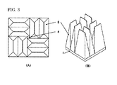
- each of the oblong rectangular pyramidal parts shown in Fig. 2 is longitudinally divided into two in a manner as to provide eight wedge-shaped parts, the bottom face of which has an increased aspect ratio, arranged on the plate-shaped part 1.
- the volume proportion of the absorber per unit spatial volume increases as compared with the configuration of Fig. 2 , and, as a result, the wave absorption characteristics in a relatively low frequency range of from 1 GHz to ten or so gigahertz are improved.
- the arrangement of the wedge-shaped parts constituting the absorber is denser than in Fig. 2 , the absorption performance for electromagnetic waves of short wavelengths (frequencies of 20 GHz or higher) is improved.
- the wave absorber according to the invention is configured such that a plurality of, basically four, oblong rectangular pyramidal (or wedge-shaped) parts 5 with an oblong rectangular bottom face are arranged on the plate-shaped part 1 while leaving a flat square space 4 in the center of the part 1.
- the manner of dividing the unit rectangular pyramid is not limited to that shown in Fig. 3 . That is, the unit rectangular pyramid may be divided into more than two rectangular pyramids and may be divided along the longitudinal direction of the bottom face or a direction perpendicular to the longitudinal direction.
- the height of the wave absorber of the invention is not particularly limited, the invention is preferably applied to small-sized wave absorbers with a height of 200 mm or less.
- the oblong rectangular pyramidal parts used in the invention may be molded from any known electromagnetic radiation absorbing material.
- the invention is applicable to wave absorbers made of either of a dielectric loss material and a magnetic loss material.
- the wave absorber may be of hybrid type composed of a plate-shaped part made of a magnetic absorbing material, such as a ferrite tile, and oblong rectangular pyramidal parts made of a dielectric loss material, or both the plate-shaped part and the rectangular pyramidal parts may be made of the same material.
- Examples of useful dielectric loss materials include resinous materials, such as carbon-containing foamed polyurethane, carbon-containing foamed polystyrene, and carbon-containing foamed polypropylene; and inorganic materials (e.g., cement, alumina, zirconia, and silica) having carbon dispersed therein. These materials may be molded into either solid or hollow shapes. Otherwise, plate-shaped molded pieces made of a resin material, an inorganic material (e.g., alumina, zirconia, or silica), paper, or a like material each containing carbon or coated with a carbon layer may be assembled to form a hollow oblong rectangular pyramid. Examples of the carbon material include graphite, carbon black, and carbon nanotubes.
- resinous materials such as carbon-containing foamed polyurethane, carbon-containing foamed polystyrene, and carbon-containing foamed polypropylene
- inorganic materials e.g., cement, alumina, zirconia
- Examples of commonly used magnetic loss materials include ferrite powder-containing resins and ferrite powder-containing inorganic materials, which are molded into either solid or hollow parts.
- a hollow oblong rectangular pyramid may be formed by assembling plate-shaped molded pieces made of a resin material, an inorganic material, such as alumina, zirconia, or silica, paper, or a like material each containing ferrite powder or coated with a ferrite layer.
- Examples of the ferrite powder include spinel ferrites, such as Ni-Zn ferrite, Li-Zn ferrite, and Mn-Zn ferrite.
- the electromagnetic radiation absorbing materials recited is a material mainly containing cement and carbon nanotubes.
- the wave absorber is usually produced by mixing carbon nanotubes and a dispersing medium, such as water, into a cement raw material, followed by stirring to prepare a slurry, casting the resulting cement slurry into a mold, curing the cement for a prescribed time under controlled temperature and humidity in accordance with the curing conditions of the cement to harden the cement, and removing the hardened block from the mold.
- the sintering step as is needed for ceramic materials is omitted, the problems associated with sintering, such as dimensional variations due to shrinkage and combustion of carbon nanotubes, are not involved, and there is obtained an incombustible and power-durable wave absorber. Furthermore, the wave absorber made from this material exhibits excellent electrical conduction characteristics even with a reduced amount of carbon based on the ionic conduction by the ions present in the water in voids of the cement matrix and electrically conductive paths formed by wave absorbing carbon nanotubes.
- the absorber In the absorber made from this material, there are electrically conductive paths that are electrically insulated from one another and each formed of a plurality of carbon nanotubes thereby to provide a resistor/capacitor (condenser) mixed structure exhibiting excellent dielectric characteristics based on resistance loss and dielectric loss. Therefore, the absorber achieves excellent radiation absorption characteristics even with a small size in the frequency range of from several to several tens of gigahertz where dielectric characteristics are dominant and in the frequency range of from several tens to several hundreds of gigahertz where electrical conduction characteristics are dominant.
- a wave absorber was made using the same material and the same method as in Example 1, except for the geometry and arrangement of the pyramids. That is, four square pyramids measuring 45 mm along each side of the bottom face and 180 mm in height were placed 2.5 mm inside from the four sides of the plate (100 mm ⁇ 100 mm ⁇ 15 mm (thickness)) with a gap (flat space) of 5 mm between adjacent pyramids. A total of 36 wave absorbers were made in that way and arrayed in a grid extending 600 mm by 600 mm. The electromagnetic wave absorbing performance of the array of the absorbers was evaluated for normal incidence by the same method as used in Example 1. The results are shown in Table 1.
- a wave absorber was made using the same material and the same method as in Comparative Example 1, except that four square pyramids measuring 50 mm along each side of the bottom face and 180 mm in height were arranged on the plate with no space therebetween. A total of 36 wave absorbers were made in that way and arrayed in a grid extending 600 mm by 600 mm. The electromagnetic wave absorbing performance of the array of the absorbers was evaluated for oblique incidence by the same method as used in Example 1. The results are shown in Table 1. Evaluation of Electromagnetic Wave Absorption Characteristics:
- electromagnetic radiation emitted from a horn antenna was collimated into plane waves by a dielectric lens so as to be directed perpendicularly to the absorbers.
- electromagnetic radiation emitted from a horn antenna was collimated into plane waves by a dielectric lens in the same manner as for the evaluation of normal incidence characteristics, and the plane waves were directed to the absorbers at an angle of incidence of 15°, 30°, and 45°.
- the measuring frequency range was from 1 to 110 GHz.
- the absorber of Comparative Example 1 having the pyramidal parts arranged with a gap therebetween proved inferior to that of Example 1 in radiation absorption characteristics for normal incidence in the entire measuring frequency range and, in particular, failed to achieve sufficient absorption characteristics in the frequency range of 5 GHz or lower. This is believed to be due to the refection of electromagnetic waves on the flat portions (gaps) between the pyramidal parts.
- Example 1 also proved superior to that of Comparative Example 2 having the pyramidal parts arranged on the plate with no gap therebetween in electromagnetic radiation absorbing performance at every angle of incidence at every measuring frequency.
Landscapes
- Engineering & Computer Science (AREA)
- Microelectronics & Electronic Packaging (AREA)
- Power Engineering (AREA)
- Shielding Devices Or Components To Electric Or Magnetic Fields (AREA)
Applications Claiming Priority (1)
| Application Number | Priority Date | Filing Date | Title |
|---|---|---|---|
| JP2012155096A JP5479540B2 (ja) | 2012-07-10 | 2012-07-10 | 電波吸収体 |
Publications (2)
| Publication Number | Publication Date |
|---|---|
| EP2685802A2 true EP2685802A2 (de) | 2014-01-15 |
| EP2685802A3 EP2685802A3 (de) | 2015-06-03 |
Family
ID=48747450
Family Applications (1)
| Application Number | Title | Priority Date | Filing Date |
|---|---|---|---|
| EP13175682.7A Withdrawn EP2685802A3 (de) | 2012-07-10 | 2013-07-09 | Absorber elektromagnetischer Wellen |
Country Status (5)
| Country | Link |
|---|---|
| US (1) | US9263802B2 (de) |
| EP (1) | EP2685802A3 (de) |
| JP (1) | JP5479540B2 (de) |
| KR (1) | KR101420059B1 (de) |
| CN (1) | CN103547134B (de) |
Families Citing this family (12)
| Publication number | Priority date | Publication date | Assignee | Title |
|---|---|---|---|---|
| JP6505570B2 (ja) * | 2015-09-30 | 2019-04-24 | 株式会社ジェイエスピー | 発泡粒子成形体及びこれを用いた電波吸収体 |
| JP6399363B2 (ja) * | 2016-05-02 | 2018-10-03 | パウダーテック株式会社 | フェライト粉末、樹脂組成物、電磁波シールド材、電子回路基板、電子回路部品及び電子機器筐体 |
| JP6786106B2 (ja) * | 2016-12-26 | 2020-11-18 | 学校法人日本大学 | 電波暗箱 |
| CN106597129B (zh) * | 2017-01-12 | 2024-02-02 | 深圳市通用测试系统有限公司 | 一种微波暗室 |
| CN108260338A (zh) * | 2018-01-17 | 2018-07-06 | 西安锐派机电设备有限公司 | 一种吸波箱 |
| US12022642B2 (en) | 2018-08-21 | 2024-06-25 | Laird Technologies, Inc. | Patterned electromagnetic interference (EMI) mitigation materials including carbon nanotubes |
| KR102012415B1 (ko) | 2019-04-24 | 2019-08-20 | (주)한국전자파연구소 | 광대역 전자파 흡수체 및 그의 제조 방법 |
| CN112909570B (zh) * | 2021-02-06 | 2022-06-28 | 中北大学 | 一种集多种吸收机制于一体的三维宽频吸波超材料 |
| CN112909571B (zh) * | 2021-02-06 | 2022-06-03 | 中北大学 | 一种兼具多种类型超材料优势的组合吸波复合材料 |
| CN115832717A (zh) * | 2022-10-27 | 2023-03-21 | 航天科工武汉磁电有限责任公司 | 兼具宽频吸收和高承载性能的吸波体及其制备方法 |
| US20240251536A1 (en) * | 2022-12-23 | 2024-07-25 | Industrial Technology Research Institute | Electromagnetic wave absorber |
| US12148994B1 (en) * | 2023-10-20 | 2024-11-19 | Tanvi Mitesh Shah | Radiation absorber device |
Citations (1)
| Publication number | Priority date | Publication date | Assignee | Title |
|---|---|---|---|---|
| JP2000188513A (ja) | 1998-10-15 | 2000-07-04 | Riken Corp | 複合電波吸収体およびその施工方法 |
Family Cites Families (12)
| Publication number | Priority date | Publication date | Assignee | Title |
|---|---|---|---|---|
| JP3036252B2 (ja) * | 1992-08-18 | 2000-04-24 | ティーディーケイ株式会社 | 電波吸収体及び該電波吸収体を用いた電波吸収壁 |
| US5373296A (en) * | 1992-08-18 | 1994-12-13 | Tdk Corporation | Electromagnetic wave absorber and wave absorption structure |
| KR0158081B1 (ko) * | 1995-07-14 | 1998-12-01 | 정명세 | 복합형 광대역 전자파 흡수체 |
| KR100325918B1 (ko) | 2000-01-27 | 2002-02-27 | 다까하시 미찌하루 | 광대역 페라이트 전파흡수체 |
| KR20010096998A (ko) * | 2000-04-19 | 2001-11-08 | 김상면 | 페라이트와 결합재의 복합재료를 이용한 광대역 전파흡수체 |
| JP2003229691A (ja) * | 2002-01-31 | 2003-08-15 | Riken Corp | 電波吸収体 |
| JP3708885B2 (ja) * | 2002-02-21 | 2005-10-19 | 三菱電線工業株式会社 | 電波音波吸収体 |
| CN100484384C (zh) | 2002-12-25 | 2009-04-29 | 东丽株式会社 | 电波吸收体用板材及电波吸收体 |
| JP4346360B2 (ja) * | 2002-12-25 | 2009-10-21 | 東レ株式会社 | 電波吸収体用シート材および電波吸収体 |
| JP4375987B2 (ja) * | 2003-03-26 | 2009-12-02 | Tdk株式会社 | 電波吸収体用成型体およびその製造方法、ならびに電波吸収体 |
| CN2666100Y (zh) * | 2003-11-24 | 2004-12-22 | 王万勋 | 电波吸收体 |
| RU2013121424A (ru) * | 2010-11-18 | 2014-12-27 | 3М Инновейтив Пропертиз Компани | Изолятор электромагнитных волн |
-
2012
- 2012-07-10 JP JP2012155096A patent/JP5479540B2/ja active Active
-
2013
- 2013-07-09 KR KR1020130080312A patent/KR101420059B1/ko not_active Expired - Fee Related
- 2013-07-09 US US13/937,655 patent/US9263802B2/en not_active Expired - Fee Related
- 2013-07-09 EP EP13175682.7A patent/EP2685802A3/de not_active Withdrawn
- 2013-07-10 CN CN201310288187.5A patent/CN103547134B/zh not_active Expired - Fee Related
Patent Citations (1)
| Publication number | Priority date | Publication date | Assignee | Title |
|---|---|---|---|---|
| JP2000188513A (ja) | 1998-10-15 | 2000-07-04 | Riken Corp | 複合電波吸収体およびその施工方法 |
Also Published As
| Publication number | Publication date |
|---|---|
| US20140132440A1 (en) | 2014-05-15 |
| EP2685802A3 (de) | 2015-06-03 |
| CN103547134A (zh) | 2014-01-29 |
| KR20140007770A (ko) | 2014-01-20 |
| JP2014017425A (ja) | 2014-01-30 |
| CN103547134B (zh) | 2015-04-01 |
| JP5479540B2 (ja) | 2014-04-23 |
| KR101420059B1 (ko) | 2014-07-15 |
| US9263802B2 (en) | 2016-02-16 |
Similar Documents
| Publication | Publication Date | Title |
|---|---|---|
| US9263802B2 (en) | Electromagnetic wave absorber | |
| US9276326B2 (en) | Electromagnetic wave absorber | |
| JP3041295B1 (ja) | 複合電波吸収体およびその施工方法 | |
| JP5496879B2 (ja) | 複合型電波吸収体 | |
| CN104582458A (zh) | 吸波超材料 | |
| US6359581B2 (en) | Electromagnetic wave abosrber | |
| US7471233B2 (en) | Electromagnetic wave absorber | |
| CN114069250A (zh) | 偶极子共振电阻式吸收器 | |
| KR0158081B1 (ko) | 복합형 광대역 전자파 흡수체 | |
| JP2001127483A (ja) | 電波吸収体 | |
| EP0618640A1 (de) | Verbesserte Abstimmung für dielektrische Materialien mit niedrigen Dielektrizitätskonstanten | |
| US6943286B1 (en) | Electromagnetic wave absorber molding material, electromagnetic wave absorber molded element and method of manufacturing same, and electromagnetic wave absorber | |
| CN1128485C (zh) | 电磁波吸收板及其制造材料 | |
| CN216389735U (zh) | 一种立体式高频透波低频吸波的频率选择结构 | |
| WO2011016109A1 (ja) | 電波吸収体 | |
| CN1909774A (zh) | 电波吸收件、电波吸收体及其制造方法、以及电波暗室 | |
| US5543796A (en) | Broadband microwave absorber | |
| JP5441211B2 (ja) | 複合型電波吸収体とそれを用いた電波吸収壁、電波暗室 | |
| JP4420253B2 (ja) | 電波吸収体及び電波暗室 | |
| JP3252571U (ja) | 電波吸収体 | |
| JPH10275996A (ja) | 電波吸収体 | |
| GB2434251A (en) | Absorber | |
| JP2609422B2 (ja) | 広帯域電波吸収体 | |
| JP4617830B2 (ja) | 電波吸収体用部材及び電波吸収体 | |
| JP4338460B2 (ja) | 電波吸収体およびその製造方法 |
Legal Events
| Date | Code | Title | Description |
|---|---|---|---|
| PUAI | Public reference made under article 153(3) epc to a published international application that has entered the european phase |
Free format text: ORIGINAL CODE: 0009012 |
|
| AK | Designated contracting states |
Kind code of ref document: A2 Designated state(s): AL AT BE BG CH CY CZ DE DK EE ES FI FR GB GR HR HU IE IS IT LI LT LU LV MC MK MT NL NO PL PT RO RS SE SI SK SM TR |
|
| AX | Request for extension of the european patent |
Extension state: BA ME |
|
| PUAL | Search report despatched |
Free format text: ORIGINAL CODE: 0009013 |
|
| AK | Designated contracting states |
Kind code of ref document: A3 Designated state(s): AL AT BE BG CH CY CZ DE DK EE ES FI FR GB GR HR HU IE IS IT LI LT LU LV MC MK MT NL NO PL PT RO RS SE SI SK SM TR |
|
| AX | Request for extension of the european patent |
Extension state: BA ME |
|
| RIC1 | Information provided on ipc code assigned before grant |
Ipc: H05K 9/00 20060101AFI20150211BHEP Ipc: H01Q 17/00 20060101ALI20150211BHEP |
|
| PUAF | Information related to the publication of a search report (a3 document) modified or deleted |
Free format text: ORIGINAL CODE: 0009199SEPU |
|
| PUAL | Search report despatched |
Free format text: ORIGINAL CODE: 0009013 |
|
| D17D | Deferred search report published (deleted) | ||
| AK | Designated contracting states |
Kind code of ref document: A3 Designated state(s): AL AT BE BG CH CY CZ DE DK EE ES FI FR GB GR HR HU IE IS IT LI LT LU LV MC MK MT NL NO PL PT RO RS SE SI SK SM TR |
|
| AX | Request for extension of the european patent |
Extension state: BA ME |
|
| RIC1 | Information provided on ipc code assigned before grant |
Ipc: H01Q 17/00 20060101ALI20150428BHEP Ipc: H05K 9/00 20060101AFI20150428BHEP |
|
| 17P | Request for examination filed |
Effective date: 20151026 |
|
| RBV | Designated contracting states (corrected) |
Designated state(s): AL AT BE BG CH CY CZ DE DK EE ES FI FR GB GR HR HU IE IS IT LI LT LU LV MC MK MT NL NO PL PT RO RS SE SI SK SM TR |
|
| 17Q | First examination report despatched |
Effective date: 20160211 |
|
| STAA | Information on the status of an ep patent application or granted ep patent |
Free format text: STATUS: THE APPLICATION IS DEEMED TO BE WITHDRAWN |
|
| 18D | Application deemed to be withdrawn |
Effective date: 20160622 |