EP2687066B1 - Appareil de transfert de tension d'entrée pour un système d'éclairage à diode électroluminescente - Google Patents
Appareil de transfert de tension d'entrée pour un système d'éclairage à diode électroluminescente Download PDFInfo
- Publication number
- EP2687066B1 EP2687066B1 EP11861770.3A EP11861770A EP2687066B1 EP 2687066 B1 EP2687066 B1 EP 2687066B1 EP 11861770 A EP11861770 A EP 11861770A EP 2687066 B1 EP2687066 B1 EP 2687066B1
- Authority
- EP
- European Patent Office
- Prior art keywords
- voltage
- input voltage
- transfer system
- storage unit
- source
- Prior art date
- Legal status (The legal status is an assumption and is not a legal conclusion. Google has not performed a legal analysis and makes no representation as to the accuracy of the status listed.)
- Not-in-force
Links
Images

Classifications
-
- H—ELECTRICITY
- H05—ELECTRIC TECHNIQUES NOT OTHERWISE PROVIDED FOR
- H05B—ELECTRIC HEATING; ELECTRIC LIGHT SOURCES NOT OTHERWISE PROVIDED FOR; CIRCUIT ARRANGEMENTS FOR ELECTRIC LIGHT SOURCES, IN GENERAL
- H05B45/00—Circuit arrangements for operating light-emitting diodes [LED]
- H05B45/30—Driver circuits
- H05B45/37—Converter circuits
-
- H—ELECTRICITY
- H05—ELECTRIC TECHNIQUES NOT OTHERWISE PROVIDED FOR
- H05B—ELECTRIC HEATING; ELECTRIC LIGHT SOURCES NOT OTHERWISE PROVIDED FOR; CIRCUIT ARRANGEMENTS FOR ELECTRIC LIGHT SOURCES, IN GENERAL
- H05B45/00—Circuit arrangements for operating light-emitting diodes [LED]
- H05B45/30—Driver circuits
- H05B45/357—Driver circuits specially adapted for retrofit LED light sources
- H05B45/3574—Emulating the electrical or functional characteristics of incandescent lamps
- H05B45/3575—Emulating the electrical or functional characteristics of incandescent lamps by means of dummy loads or bleeder circuits, e.g. for dimmers
-
- Y—GENERAL TAGGING OF NEW TECHNOLOGICAL DEVELOPMENTS; GENERAL TAGGING OF CROSS-SECTIONAL TECHNOLOGIES SPANNING OVER SEVERAL SECTIONS OF THE IPC; TECHNICAL SUBJECTS COVERED BY FORMER USPC CROSS-REFERENCE ART COLLECTIONS [XRACs] AND DIGESTS
- Y02—TECHNOLOGIES OR APPLICATIONS FOR MITIGATION OR ADAPTATION AGAINST CLIMATE CHANGE
- Y02B—CLIMATE CHANGE MITIGATION TECHNOLOGIES RELATED TO BUILDINGS, e.g. HOUSING, HOUSE APPLIANCES OR RELATED END-USER APPLICATIONS
- Y02B20/00—Energy efficient lighting technologies, e.g. halogen lamps or gas discharge lamps
- Y02B20/30—Semiconductor lamps, e.g. solid state lamps [SSL] light emitting diodes [LED] or organic LED [OLED]
Definitions
- the present disclosure relates to an input voltage transfer apparatus for a Light Emitting Diode (LED) lighting system.
- LED Light Emitting Diode
- LEDs are semiconductor devices, LEDs have long service life, fast lighting speed, low consumption power, and excellent color reproductivity.
- LEDs are robust to impact, and it is easy to miniaturize and thin LEDs.
- EP2288237A2 and WO2005/115058A1 disclose circuits for lighting devices.
- Embodiments provide an input voltage transfer apparatus for an LED lighting system, which turns on a switching element when a zero voltage is inputted as an input voltage, turns on a separate switching element when a non-zero voltage is inputted in a state where the switching element is being turned on, turns on the switching element, which has been turned on when the zero voltage is inputted, for a certain time, and thus can efficiently maintain dimming and prevent flicker from occurring in an LED.
- an input voltage transfer apparatus for an LED lighting system includes: a source voltage storage unit storing a source voltage; a zero voltage switching unit turning on according to the source voltage stored in the source voltage storage unit when a zero voltage is inputted; and a nonzero voltage switching unit turning on according to a current applied thereto through the zero voltage switching unit when a nonzero voltage is inputted, wherein when the nonzero voltage switching unit is turned on, the source voltage storage unit discharges the stored source voltage.
- an input voltage transfer apparatus for an LED lighting system includes: a source voltage storage unit storing a source voltage; a zero voltage switching unit turning on according to the source voltage stored in the source voltage storage unit when a zero voltage is inputted; a shutdown signal supply unit receiving the source voltage to supply a shutdown signal for shutting down a control circuit, when the zero voltage is inputted thereto; and a nonzero voltage switching unit turning on according to a current applied thereto through the zero voltage switching unit when a nonzero voltage is inputted, wherein when the nonzero voltage switching unit is turned on, the shutdown signal supply unit is turned off, and the source voltage storage unit discharges the stored source voltage.
- the input voltage transfer apparatus for an LED lighting system turns on a switching element when a zero voltage is inputted as an input voltage, turns on a separate switching element when a non-zero voltage is inputted in a state where the switching element is being turned on, turns on the switching element, which has been turned on when the zero voltage is inputted, for a certain time, and thus can efficiently maintain dimming and prevent flicker from occurring in an LED.
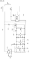
- Fig 1 is a circuit diagram illustrating an input voltage transfer apparatus for an LED lighting system, according to an embodiment.
- Fig 2 is a diagram showing a waveform of an input voltage which is inputted to an input voltage transfer apparatus for an LED lighting system according to an embodiment.
- Fig 3 is a circuit diagram illustrating a modification example of an input voltage transfer apparatus for an LED lighting system according to an embodiment.
- an input voltage transfer apparatus 200 for an LED lighting system may include a source voltage storage unit 220, a zero voltage switching unit 210, a shutdown signal supply unit 230, and a nonzero voltage switching unit 240.
- the source voltage storage unit 220 stores a source voltage VCC transferred through a resistor R2, in which state the source voltage storage unit 220 discharges the stored source voltage VCC when the nonzero voltage switching unit 240 is turned on.
- the source voltage storage unit 220 includes a first resistor R4 and a first capacitor C2.
- the resistor R2 transfers the source voltage VCC to the source voltage storage unit 220.
- the zero voltage switching unit 210 is turned on when a zero voltage is inputted through a bridge circuit 100 (Vin during time t0 - t1 in Fig. 2 ), but when a nonzero voltage is inputted through the bridge circuit 100 (Vin during time t1 t2 in Fig. 2 ), the zero voltage switching unit 210 applies a current to the nonzero voltage switching unit 240.
- the zero voltage switching unit 210 includes an n-channel metal oxide semiconductor (NMOS) transistor Q1 or an NPN bipolar junction transistor.
- NMOS metal oxide semiconductor
- the resistor R1 transfers an input voltage Vin.
- the source voltage storage unit 220 discharges a stored source voltage VCC, and thus, when a voltage stored in the first capacitor C2 is shifted to less than a threshold voltage of the NMOS transistor Q1, the zero voltage switching unit 210 is turned off.
- a turned-off time of the zero voltage switching unit 210 may be adjusted by regulating a time constant R4 ⁇ C2 of the source voltage storage unit 220. That is, even when the zero voltage is inputted and then the nonzero voltage is inputted, the zero voltage switching unit 210 is not turned off but is turned on proportional to the time constant R4 ⁇ C2 and then turned off. Accordingly, even when the zero voltage is inputted and then the nonzero voltage is inputted, the zero voltage switching unit 210 and the nonzero voltage switching unit 240 are simultaneously turned on during the time constant R4 ⁇ C2 thereby applying a current.
- the shutdown signal supply unit 230 is turned on by the source voltage VCC that is applied thereto when the zero voltage is inputted, and supplies a shutdown signal SD for shutting down a control circuit 400 to the control circuit 400. However, when the nonzero voltage switching unit 240 is turned on, the shutdown signal supply unit 230 is turned off and does no longer supply the shutdown signal SD.
- the shutdown signal supply unit 230 may include a p-channel MOS (PMOS) transistor or a PNP bipolar junction transistor Q2.
- the shutdown signal supply unit 230 may further include a Zener diode Z1 connected between a base of the PNP bipolar junction transistor Q2 and a ground.
- a resistor R3 transfers the source voltage VCC.
- the nonzero voltage switching unit 240 When the nonzero voltage is inputted (Vin during time t1 t2 in Fig. 2 ), the nonzero voltage switching unit 240 is turned on by a current that is applied thereto through the zero voltage switching unit 210.
- the source voltage VCC is no longer applied to the source voltage storage unit 220 and the shutdown signal supply unit 230.
- the source voltage storage unit 220 discharges a stored source voltage VCC, and the shutdown signal supply unit 230 does not supply the shutdown signal SD.
- the nonzero voltage switching unit 240 includes an NMOS transistor or an NPN bipolar junction transistor Q3. Resistors R5 to R7 transfer a current that is applied by the zero voltage switching unit 210. A capacitor C3 prevents a noise signal from being applied.
- the zero voltage switching unit 210 is turned on when the zero voltage is inputted as the input voltage, and then when the nonzero voltage is inputted, the zero voltage switching unit 210 is not immediately turned off but is turned on proportional to the time constant R4 ⁇ C2 and then turned off, thus more efficiently maintaining dimming.
- the input voltage transfer apparatus 200 can more efficiently maintain dimming, and thus prevent flicker from occurring in an LED.
- the input voltage transfer apparatus 200 may further include a reverse-current prevention unit 250 that prevents a current from being reversely applied to the zero voltage switching unit 210.
- the reverse-current prevention unit 250 includes a diode D1 that has a cathode connected to a resistor, and an anode connected to the ground.
- the input voltage transfer apparatus 200 may further include an auxiliary storage unit 260 that stores an applied source voltage VCC while the zero voltage is being inputted and then discharges the stored source voltage VCC while the nonzero voltage is being inputted.
- the auxiliary storage unit 260 includes a second capacitor C1.
- a modification example 1200 of the input voltage transfer apparatus 200 according to an embodiment will be described below with reference to Fig. 3 .
- the modification example 1200 only a difference between the input voltage transfer apparatus 200 and the modification example 1200 will be described below.
- the modification example 1200 of the input voltage transfer apparatus 200 includes a shutdown signal supply unit 1230.
- the shutdown signal supply unit 1230 includes an NMOS transistor or an NPN bipolar junction transistor Q12.
- the shutdown signal supply unit 1230 may further include a Zener diode Z11 connected between a base of the NPN bipolar junction transistor Q12 and a resistor R12.
- a resistor R13 transfers the source voltage VCC.
- the input voltage transfer apparatus for an LED lighting system turns on a switching element when a zero voltage is inputted as an input voltage, turns on a separate switching element when a non-zero voltage is inputted in a state where the switching element is being turned on, turns on the switching element, which has been turned on when the zero voltage is inputted, for a certain time, and thus can efficiently maintain dimming and prevent flicker from occurring in an LED.
Landscapes
- Circuit Arrangement For Electric Light Sources In General (AREA)
- Led Devices (AREA)
- Electronic Switches (AREA)
Claims (14)
- Système de transfert de tension d'entrée pour un système d'éclairage à DEL, ledit système de transfert de tension d'entrée comprenant :un circuit en pont (100) qui redresse une tension d'entrée (Vin) qui est couplé au système d'éclairage à diode électroluminescente, et dans lequel la tension d'entrée (Vin) alimente une première et une deuxième borne du circuit en pont (100) ;caractérisé en ce que le système de transfert de tension d'entrée comprend en outre :
un appareil de transfert de tension d'entrée (200), qui comprend :une unité de stockage de tension source (220), dont une première entrée est connectée à une source de tension (VCC) pour stocker une tension source ;une unité de commutation de tension nulle (210), dont une première borne est connectée à une quatrième borne du circuit en pont (100) et dont une deuxième borne est connectée à une sortie de l'unité de stockage de tension source (220) et dont une troisième borne est connectée à la terre ;une unité de commutation de tension non nulle (240), dont une première borne est connectée à une troisième borne du circuit en pont (100) et dont une deuxième borne est connectée à la première entrée de l'unité de stockage de tension source (220) et dont une troisième borne est connectée à la terre ;dans lequel l'appareil de transfert de tension d'entrée (200) est configuré pour allumer l'unité de commutation de tension nulle (210) lorsque la tension entrée (Vin) est nulle et en se basant sur la tension source stockée dans l'unité de stockage de tension source (220) ; et est configuré pour ensuite allumer l'unité de commutation de tension non nulle (240) lorsque la tension entrée est non nulle et un courant est appliqué sur celle-ci par l'intermédiaire de l'unité de commutation de tension nulle (210) ;grâce à quoi l'appareil de transfert de tension d'entrée (200) est en outre configuré pour ensuite décharger l'unité de stockage de tension source (220) lorsque l'unité de commutation de tension non nulle (240) s'allume, et ensuite pour éteindre l'unité de commutation de tension nulle (210), lorsqu'un niveau de la tension source stockée dans l'unité de stockage de la tension source est inférieur à une tension de seuil. - Système de transfert de tension d'entrée selon la revendication 1, dans lequel l'unité de stockage de tension source (220) comprend une première résistance (R4) et un premier condensateur (C2).
- Système de transfert de tension d'entrée selon au moins l'une de la revendication 1 et de la revendication 2, dans lequel l'unité de commutation de tension nulle (210) comprend un transistor MOS (Q1) ou un transistor à jonctions bipolaires.
- Système de transfert de tension d'entrée selon au moins l'une des revendication 1 à revendication 3,
dans lequel l'unité de commutation de tension non nulle (240) comprend un transistor MOS ou un transistor à jonctions bipolaires. - Système de transfert de tension d'entrée selon au moins l'une des revendication 1 à revendication 4, comprenant en outre une diode (D1) ;
dans lequel une anode de la diode (D1) est connectée à la terre et une cathode de la diode est connectée à l'unité de stockage de la tension source. - Système de transfert de tension d'entrée selon au moins l'une des revendication 1 à revendication 5, comprenant en outre une unité de stockage auxiliaire qui stocke la tension source qui est transférée sur celle-ci lorsque la tension d'entrée (Vin) de la tension nulle est entrée.
- Système de transfert de tension d'entrée selon la revendication 6, dans lequel l'unité de stockage auxiliaire comprend un deuxième condensateur (C12).
- Système de transfert de tension d'entrée selon la revendication 7, ledit système de transfert de tension d'entrée comprenant en outre :un convertisseur CC-CC (300) qui règle le niveau d'une tension d'entrée (Vin) redressée et qui transfère la tension d'entrée réglée sur les diodes électroluminescentes,un circuit de commande (400) qui commande le fonctionnement du convertisseur CC-CC (300),l'appareil de transfert de tension d'entrée (200), qui comprend en outre :une unité de fourniture de signal de fermeture (230) connectée à la tension source et à la deuxième borne de l'unité de stockage de tension source (220),dans lequel l'unité de fourniture de signal de fermeture (230) est configurée pourrecevoir la tension source pour fournir un signal de fermeture pour fermer le circuit de commande (400), lorsque la tension entrée (Vin) est nulle,et ensuite, lorsque l'unité de commutation de tension non nulle (240) est allumée, l'unité de fourniture de signal de fermeture (230) est ensuite éteinte, et l'unité de stockage de tension source (220) décharge la tension source stockée.
- Système de transfert de tension d'entrée selon la revendication 8, dans lequel l'unité de fourniture de signal de fermeture (230) comprend un transistor PMOS ou un transistor à jonctions bipolaires PNP.
- Système de transfert de tension d'entrée selon la revendication 9, dans lequel l'unité de fourniture de signal de fermeture (230) comprend en outre une diode Zener connectée entre une base du transistor à jonctions bipolaires PNP et la terre.
- Système de transfert de tension d'entrée selon la revendication 2,
dans lequel l'unité de commutation de tension nulle (210) est allumée en fonction d'une constante de temps de la première résistance et du premier condensateur. - Système de transfert de tension d'entrée selon la revendication 8, dans lequel l'unité de fourniture de signal de fermeture (230) comprend un transistor NMOS ou un transistor à jonctions bipolaires NPN.
- Système de transfert de tension d'entrée selon la revendication 12, dans lequel l'unité de fourniture de signal de fermeture (230) comprend en outre une diode Zener connectée entre une base du transistor à jonctions bipolaires NPN et l'unité de stockage de la tension source.
- Système de transfert de tension d'entrée selon la revendication 13, ladite unité de fourniture de signal de fermeture (230) comprenant en outre :
une deuxième résistance connectée entre une base du transistor à jonctions bipolaires NPN et la terre.
Applications Claiming Priority (2)
| Application Number | Priority Date | Filing Date | Title |
|---|---|---|---|
| KR1020110024492A KR101174010B1 (ko) | 2011-03-18 | 2011-03-18 | 발광 다이오드 조명 시스템용 입력 전압 전달 장치 |
| PCT/KR2011/007490 WO2012128436A1 (fr) | 2011-03-18 | 2011-10-10 | Appareil de transfert de tension d'entrée pour système d'éclairage à diode électroluminescente |
Publications (3)
| Publication Number | Publication Date |
|---|---|
| EP2687066A1 EP2687066A1 (fr) | 2014-01-22 |
| EP2687066A4 EP2687066A4 (fr) | 2014-09-03 |
| EP2687066B1 true EP2687066B1 (fr) | 2019-08-28 |
Family
ID=46879551
Family Applications (1)
| Application Number | Title | Priority Date | Filing Date |
|---|---|---|---|
| EP11861770.3A Not-in-force EP2687066B1 (fr) | 2011-03-18 | 2011-10-10 | Appareil de transfert de tension d'entrée pour un système d'éclairage à diode électroluminescente |
Country Status (6)
| Country | Link |
|---|---|
| US (1) | US8981659B2 (fr) |
| EP (1) | EP2687066B1 (fr) |
| KR (1) | KR101174010B1 (fr) |
| CN (1) | CN103548422B (fr) |
| TW (1) | TWI479943B (fr) |
| WO (1) | WO2012128436A1 (fr) |
Family Cites Families (19)
| Publication number | Priority date | Publication date | Assignee | Title |
|---|---|---|---|---|
| JP3630019B2 (ja) | 1999-06-25 | 2005-03-16 | 松下電工株式会社 | 2線式配線器具 |
| JP2002354790A (ja) | 2001-05-21 | 2002-12-06 | Sanken Electric Co Ltd | コンバータ及びその起動方法 |
| DE10315474A1 (de) | 2003-04-04 | 2004-10-21 | Patent-Treuhand-Gesellschaft für elektrische Glühlampen mbH | Verfahren zum Variieren der Leistungsaufnahme von kapazitiven Lasten |
| EP1752022A1 (fr) * | 2004-05-19 | 2007-02-14 | Polybrite International, Inc. | Circuit de gradation pour del comprenant un moyen permettant de maintenir le courant dans un triac |
| JP2006319172A (ja) * | 2005-05-13 | 2006-11-24 | Wako Denken Kk | Ledランプ調光用アダプタ装置 |
| GB0617393D0 (en) | 2006-09-04 | 2006-10-11 | Lutron Electronics Co | Variable load circuits for use with lighting control devices |
| US8106597B2 (en) * | 2008-01-22 | 2012-01-31 | Supertex, Inc. | High efficiency boost LED driver with output |
| CN101227778B (zh) | 2008-02-19 | 2011-12-14 | 东南大学 | 一种自激振荡式大功率led恒流驱动电路 |
| US8829812B2 (en) | 2008-04-04 | 2014-09-09 | Koninklijke Philips N.V. | Dimmable lighting system |
| TWI399122B (zh) | 2008-08-20 | 2013-06-11 | Univ Nat Sun Yat Sen | 單級具零電壓切換之led驅動電路 |
| KR100877521B1 (ko) | 2008-08-26 | 2009-01-07 | 엔 하이테크 주식회사 | 엘이디 조명 구동회로 |
| EP2257124B1 (fr) * | 2009-05-29 | 2018-01-24 | Silergy Corp. | Circuit de connexion d'un circuit d'éclairage basse consommation à un variateur |
| CN201414240Y (zh) | 2009-06-04 | 2010-02-24 | 佛山市伊戈尔电业制造股份有限公司 | 用于led照明灯直流电源的缓冲限流电路 |
| JP2012023001A (ja) * | 2009-08-21 | 2012-02-02 | Toshiba Lighting & Technology Corp | 点灯回路及び照明装置 |
| JP5362484B2 (ja) | 2009-08-26 | 2013-12-11 | パナソニック株式会社 | 負荷制御装置 |
| JP5361610B2 (ja) * | 2009-08-26 | 2013-12-04 | パナソニック株式会社 | 負荷制御装置 |
| KR20110027328A (ko) | 2009-09-10 | 2011-03-16 | 엘지이노텍 주식회사 | 엘이디 드라이버 보호 장치 |
| CN102223749B (zh) | 2011-06-20 | 2014-06-11 | 浙江工业大学 | 一种插入式多功能led驱动电路 |
| US8575849B2 (en) * | 2011-07-15 | 2013-11-05 | Osram Sylvania Inc. | Resonate driver for solid state light sources |
-
2011
- 2011-03-18 KR KR1020110024492A patent/KR101174010B1/ko not_active Expired - Fee Related
- 2011-10-10 CN CN201180070243.7A patent/CN103548422B/zh not_active Expired - Fee Related
- 2011-10-10 US US14/005,883 patent/US8981659B2/en not_active Expired - Fee Related
- 2011-10-10 EP EP11861770.3A patent/EP2687066B1/fr not_active Not-in-force
- 2011-10-10 WO PCT/KR2011/007490 patent/WO2012128436A1/fr not_active Ceased
-
2012
- 2012-03-16 TW TW101109013A patent/TWI479943B/zh not_active IP Right Cessation
Non-Patent Citations (1)
| Title |
|---|
| None * |
Also Published As
| Publication number | Publication date |
|---|---|
| WO2012128436A1 (fr) | 2012-09-27 |
| EP2687066A1 (fr) | 2014-01-22 |
| US8981659B2 (en) | 2015-03-17 |
| US20140217925A1 (en) | 2014-08-07 |
| CN103548422B (zh) | 2015-09-30 |
| TW201249251A (en) | 2012-12-01 |
| EP2687066A4 (fr) | 2014-09-03 |
| CN103548422A (zh) | 2014-01-29 |
| KR101174010B1 (ko) | 2012-08-16 |
| TWI479943B (zh) | 2015-04-01 |
Similar Documents
| Publication | Publication Date | Title |
|---|---|---|
| US9336976B2 (en) | Relay driving device and method for driving a relay | |
| US20110122659A1 (en) | Power transistor driving circuits and methods for switching mode power supplies | |
| US20080018174A1 (en) | Power control apparatus and method thereof | |
| US8476838B2 (en) | Light source lighting circuit and lamp system for vehicle | |
| US20140097754A1 (en) | Light emitting diode luminance system having clamping device | |
| US8258971B2 (en) | Low voltage warning circuit | |
| US8686783B2 (en) | Level shifter and boost driving circuit | |
| EP3264864A1 (fr) | Circuit d'attaque de del | |
| US7573251B2 (en) | AC-to-DC voltage regulator | |
| US9705323B2 (en) | Power supply system and power control circuit thereof | |
| US8138686B2 (en) | Current regulator and method for efficiency improvement of a LED display system | |
| EP3310131B1 (fr) | Circuit de commande de diode électroluminescente | |
| US8084961B2 (en) | Backlight module control system and control method thereof | |
| EP2687066B1 (fr) | Appareil de transfert de tension d'entrée pour un système d'éclairage à diode électroluminescente | |
| US8581503B1 (en) | Method of forming an LED control circuit and structure therefor | |
| CN105719596B (zh) | 应用于显示系统的驱动电路与驱动方法及显示系统 | |
| US8415928B2 (en) | Power circuit | |
| US8569962B2 (en) | LED driver circuit and LED driver system | |
| US7592793B2 (en) | Voltage regulator providing power from AC power source | |
| US20110241754A1 (en) | Level shifter and method of controlling level shifter | |
| US10912169B2 (en) | LED lighting apparatus | |
| US20100001658A1 (en) | Light emitting diode circuit and light emitting diode driving circuit | |
| KR101044725B1 (ko) | 엔진제어유닛의 전압 레귤레이터 전원 스위칭 회로 | |
| CN102096429A (zh) | 反馈稳压装置与方法及其应用的电源转换系统 | |
| KR20170094680A (ko) | 발광 다이오드 조명 장치 |
Legal Events
| Date | Code | Title | Description |
|---|---|---|---|
| PUAI | Public reference made under article 153(3) epc to a published international application that has entered the european phase |
Free format text: ORIGINAL CODE: 0009012 |
|
| 17P | Request for examination filed |
Effective date: 20130918 |
|
| AK | Designated contracting states |
Kind code of ref document: A1 Designated state(s): AL AT BE BG CH CY CZ DE DK EE ES FI FR GB GR HR HU IE IS IT LI LT LU LV MC MK MT NL NO PL PT RO RS SE SI SK SM TR |
|
| DAX | Request for extension of the european patent (deleted) | ||
| A4 | Supplementary search report drawn up and despatched |
Effective date: 20140805 |
|
| RIC1 | Information provided on ipc code assigned before grant |
Ipc: H05B 37/02 20060101AFI20140730BHEP Ipc: H05B 33/08 20060101ALI20140730BHEP |
|
| RAP1 | Party data changed (applicant data changed or rights of an application transferred) |
Owner name: LG INNOTEK CO., LTD. |
|
| STAA | Information on the status of an ep patent application or granted ep patent |
Free format text: STATUS: EXAMINATION IS IN PROGRESS |
|
| 17Q | First examination report despatched |
Effective date: 20171012 |
|
| GRAP | Despatch of communication of intention to grant a patent |
Free format text: ORIGINAL CODE: EPIDOSNIGR1 |
|
| STAA | Information on the status of an ep patent application or granted ep patent |
Free format text: STATUS: GRANT OF PATENT IS INTENDED |
|
| INTG | Intention to grant announced |
Effective date: 20190409 |
|
| GRAS | Grant fee paid |
Free format text: ORIGINAL CODE: EPIDOSNIGR3 |
|
| GRAA | (expected) grant |
Free format text: ORIGINAL CODE: 0009210 |
|
| STAA | Information on the status of an ep patent application or granted ep patent |
Free format text: STATUS: THE PATENT HAS BEEN GRANTED |
|
| AK | Designated contracting states |
Kind code of ref document: B1 Designated state(s): AL AT BE BG CH CY CZ DE DK EE ES FI FR GB GR HR HU IE IS IT LI LT LU LV MC MK MT NL NO PL PT RO RS SE SI SK SM TR |
|
| REG | Reference to a national code |
Ref country code: GB Ref legal event code: FG4D |
|
| REG | Reference to a national code |
Ref country code: CH Ref legal event code: EP |
|
| REG | Reference to a national code |
Ref country code: DE Ref legal event code: R096 Ref document number: 602011061704 Country of ref document: DE |
|
| REG | Reference to a national code |
Ref country code: AT Ref legal event code: REF Ref document number: 1174051 Country of ref document: AT Kind code of ref document: T Effective date: 20190915 |
|
| REG | Reference to a national code |
Ref country code: IE Ref legal event code: FG4D |
|
| REG | Reference to a national code |
Ref country code: NL Ref legal event code: MP Effective date: 20190828 |
|
| REG | Reference to a national code |
Ref country code: LT Ref legal event code: MG4D |
|
| PG25 | Lapsed in a contracting state [announced via postgrant information from national office to epo] |
Ref country code: NO Free format text: LAPSE BECAUSE OF FAILURE TO SUBMIT A TRANSLATION OF THE DESCRIPTION OR TO PAY THE FEE WITHIN THE PRESCRIBED TIME-LIMIT Effective date: 20191128 Ref country code: FI Free format text: LAPSE BECAUSE OF FAILURE TO SUBMIT A TRANSLATION OF THE DESCRIPTION OR TO PAY THE FEE WITHIN THE PRESCRIBED TIME-LIMIT Effective date: 20190828 Ref country code: SE Free format text: LAPSE BECAUSE OF FAILURE TO SUBMIT A TRANSLATION OF THE DESCRIPTION OR TO PAY THE FEE WITHIN THE PRESCRIBED TIME-LIMIT Effective date: 20190828 Ref country code: HR Free format text: LAPSE BECAUSE OF FAILURE TO SUBMIT A TRANSLATION OF THE DESCRIPTION OR TO PAY THE FEE WITHIN THE PRESCRIBED TIME-LIMIT Effective date: 20190828 Ref country code: LT Free format text: LAPSE BECAUSE OF FAILURE TO SUBMIT A TRANSLATION OF THE DESCRIPTION OR TO PAY THE FEE WITHIN THE PRESCRIBED TIME-LIMIT Effective date: 20190828 Ref country code: PT Free format text: LAPSE BECAUSE OF FAILURE TO SUBMIT A TRANSLATION OF THE DESCRIPTION OR TO PAY THE FEE WITHIN THE PRESCRIBED TIME-LIMIT Effective date: 20191230 Ref country code: BG Free format text: LAPSE BECAUSE OF FAILURE TO SUBMIT A TRANSLATION OF THE DESCRIPTION OR TO PAY THE FEE WITHIN THE PRESCRIBED TIME-LIMIT Effective date: 20191128 Ref country code: NL Free format text: LAPSE BECAUSE OF FAILURE TO SUBMIT A TRANSLATION OF THE DESCRIPTION OR TO PAY THE FEE WITHIN THE PRESCRIBED TIME-LIMIT Effective date: 20190828 |
|
| PG25 | Lapsed in a contracting state [announced via postgrant information from national office to epo] |
Ref country code: ES Free format text: LAPSE BECAUSE OF FAILURE TO SUBMIT A TRANSLATION OF THE DESCRIPTION OR TO PAY THE FEE WITHIN THE PRESCRIBED TIME-LIMIT Effective date: 20190828 Ref country code: AL Free format text: LAPSE BECAUSE OF FAILURE TO SUBMIT A TRANSLATION OF THE DESCRIPTION OR TO PAY THE FEE WITHIN THE PRESCRIBED TIME-LIMIT Effective date: 20190828 Ref country code: LV Free format text: LAPSE BECAUSE OF FAILURE TO SUBMIT A TRANSLATION OF THE DESCRIPTION OR TO PAY THE FEE WITHIN THE PRESCRIBED TIME-LIMIT Effective date: 20190828 Ref country code: IS Free format text: LAPSE BECAUSE OF FAILURE TO SUBMIT A TRANSLATION OF THE DESCRIPTION OR TO PAY THE FEE WITHIN THE PRESCRIBED TIME-LIMIT Effective date: 20191228 Ref country code: RS Free format text: LAPSE BECAUSE OF FAILURE TO SUBMIT A TRANSLATION OF THE DESCRIPTION OR TO PAY THE FEE WITHIN THE PRESCRIBED TIME-LIMIT Effective date: 20190828 Ref country code: GR Free format text: LAPSE BECAUSE OF FAILURE TO SUBMIT A TRANSLATION OF THE DESCRIPTION OR TO PAY THE FEE WITHIN THE PRESCRIBED TIME-LIMIT Effective date: 20191129 |
|
| REG | Reference to a national code |
Ref country code: AT Ref legal event code: MK05 Ref document number: 1174051 Country of ref document: AT Kind code of ref document: T Effective date: 20190828 |
|
| PG25 | Lapsed in a contracting state [announced via postgrant information from national office to epo] |
Ref country code: TR Free format text: LAPSE BECAUSE OF FAILURE TO SUBMIT A TRANSLATION OF THE DESCRIPTION OR TO PAY THE FEE WITHIN THE PRESCRIBED TIME-LIMIT Effective date: 20190828 |
|
| PG25 | Lapsed in a contracting state [announced via postgrant information from national office to epo] |
Ref country code: IT Free format text: LAPSE BECAUSE OF FAILURE TO SUBMIT A TRANSLATION OF THE DESCRIPTION OR TO PAY THE FEE WITHIN THE PRESCRIBED TIME-LIMIT Effective date: 20190828 Ref country code: RO Free format text: LAPSE BECAUSE OF FAILURE TO SUBMIT A TRANSLATION OF THE DESCRIPTION OR TO PAY THE FEE WITHIN THE PRESCRIBED TIME-LIMIT Effective date: 20190828 Ref country code: PL Free format text: LAPSE BECAUSE OF FAILURE TO SUBMIT A TRANSLATION OF THE DESCRIPTION OR TO PAY THE FEE WITHIN THE PRESCRIBED TIME-LIMIT Effective date: 20190828 Ref country code: AT Free format text: LAPSE BECAUSE OF FAILURE TO SUBMIT A TRANSLATION OF THE DESCRIPTION OR TO PAY THE FEE WITHIN THE PRESCRIBED TIME-LIMIT Effective date: 20190828 Ref country code: EE Free format text: LAPSE BECAUSE OF FAILURE TO SUBMIT A TRANSLATION OF THE DESCRIPTION OR TO PAY THE FEE WITHIN THE PRESCRIBED TIME-LIMIT Effective date: 20190828 Ref country code: DK Free format text: LAPSE BECAUSE OF FAILURE TO SUBMIT A TRANSLATION OF THE DESCRIPTION OR TO PAY THE FEE WITHIN THE PRESCRIBED TIME-LIMIT Effective date: 20190828 |
|
| PG25 | Lapsed in a contracting state [announced via postgrant information from national office to epo] |
Ref country code: CZ Free format text: LAPSE BECAUSE OF FAILURE TO SUBMIT A TRANSLATION OF THE DESCRIPTION OR TO PAY THE FEE WITHIN THE PRESCRIBED TIME-LIMIT Effective date: 20190828 Ref country code: SM Free format text: LAPSE BECAUSE OF FAILURE TO SUBMIT A TRANSLATION OF THE DESCRIPTION OR TO PAY THE FEE WITHIN THE PRESCRIBED TIME-LIMIT Effective date: 20190828 Ref country code: IS Free format text: LAPSE BECAUSE OF FAILURE TO SUBMIT A TRANSLATION OF THE DESCRIPTION OR TO PAY THE FEE WITHIN THE PRESCRIBED TIME-LIMIT Effective date: 20200224 Ref country code: MC Free format text: LAPSE BECAUSE OF FAILURE TO SUBMIT A TRANSLATION OF THE DESCRIPTION OR TO PAY THE FEE WITHIN THE PRESCRIBED TIME-LIMIT Effective date: 20190828 Ref country code: SK Free format text: LAPSE BECAUSE OF FAILURE TO SUBMIT A TRANSLATION OF THE DESCRIPTION OR TO PAY THE FEE WITHIN THE PRESCRIBED TIME-LIMIT Effective date: 20190828 |
|
| REG | Reference to a national code |
Ref country code: CH Ref legal event code: PL |
|
| REG | Reference to a national code |
Ref country code: DE Ref legal event code: R097 Ref document number: 602011061704 Country of ref document: DE |
|
| PLBE | No opposition filed within time limit |
Free format text: ORIGINAL CODE: 0009261 |
|
| STAA | Information on the status of an ep patent application or granted ep patent |
Free format text: STATUS: NO OPPOSITION FILED WITHIN TIME LIMIT |
|
| PG2D | Information on lapse in contracting state deleted |
Ref country code: IS |
|
| PG25 | Lapsed in a contracting state [announced via postgrant information from national office to epo] |
Ref country code: CH Free format text: LAPSE BECAUSE OF NON-PAYMENT OF DUE FEES Effective date: 20191031 Ref country code: LU Free format text: LAPSE BECAUSE OF NON-PAYMENT OF DUE FEES Effective date: 20191010 Ref country code: LI Free format text: LAPSE BECAUSE OF NON-PAYMENT OF DUE FEES Effective date: 20191031 |
|
| 26N | No opposition filed |
Effective date: 20200603 |
|
| REG | Reference to a national code |
Ref country code: BE Ref legal event code: MM Effective date: 20191031 |
|
| PG25 | Lapsed in a contracting state [announced via postgrant information from national office to epo] |
Ref country code: BE Free format text: LAPSE BECAUSE OF NON-PAYMENT OF DUE FEES Effective date: 20191031 Ref country code: SI Free format text: LAPSE BECAUSE OF FAILURE TO SUBMIT A TRANSLATION OF THE DESCRIPTION OR TO PAY THE FEE WITHIN THE PRESCRIBED TIME-LIMIT Effective date: 20190828 |
|
| GBPC | Gb: european patent ceased through non-payment of renewal fee |
Effective date: 20191128 |
|
| PG25 | Lapsed in a contracting state [announced via postgrant information from national office to epo] |
Ref country code: GB Free format text: LAPSE BECAUSE OF NON-PAYMENT OF DUE FEES Effective date: 20191128 Ref country code: IE Free format text: LAPSE BECAUSE OF NON-PAYMENT OF DUE FEES Effective date: 20191010 Ref country code: FR Free format text: LAPSE BECAUSE OF NON-PAYMENT OF DUE FEES Effective date: 20191028 |
|
| PG25 | Lapsed in a contracting state [announced via postgrant information from national office to epo] |
Ref country code: CY Free format text: LAPSE BECAUSE OF FAILURE TO SUBMIT A TRANSLATION OF THE DESCRIPTION OR TO PAY THE FEE WITHIN THE PRESCRIBED TIME-LIMIT Effective date: 20190828 |
|
| PG25 | Lapsed in a contracting state [announced via postgrant information from national office to epo] |
Ref country code: HU Free format text: LAPSE BECAUSE OF FAILURE TO SUBMIT A TRANSLATION OF THE DESCRIPTION OR TO PAY THE FEE WITHIN THE PRESCRIBED TIME-LIMIT; INVALID AB INITIO Effective date: 20111010 Ref country code: MT Free format text: LAPSE BECAUSE OF FAILURE TO SUBMIT A TRANSLATION OF THE DESCRIPTION OR TO PAY THE FEE WITHIN THE PRESCRIBED TIME-LIMIT Effective date: 20190828 |
|
| PGFP | Annual fee paid to national office [announced via postgrant information from national office to epo] |
Ref country code: DE Payment date: 20210916 Year of fee payment: 11 |
|
| PG25 | Lapsed in a contracting state [announced via postgrant information from national office to epo] |
Ref country code: MK Free format text: LAPSE BECAUSE OF FAILURE TO SUBMIT A TRANSLATION OF THE DESCRIPTION OR TO PAY THE FEE WITHIN THE PRESCRIBED TIME-LIMIT Effective date: 20190828 |
|
| REG | Reference to a national code |
Ref country code: DE Ref legal event code: R119 Ref document number: 602011061704 Country of ref document: DE |
|
| PG25 | Lapsed in a contracting state [announced via postgrant information from national office to epo] |
Ref country code: DE Free format text: LAPSE BECAUSE OF NON-PAYMENT OF DUE FEES Effective date: 20230503 |