EP2687960A2 - Panneau d'écran tactile et procédé de commande de celui-ci - Google Patents
Panneau d'écran tactile et procédé de commande de celui-ci Download PDFInfo
- Publication number
- EP2687960A2 EP2687960A2 EP13152776.4A EP13152776A EP2687960A2 EP 2687960 A2 EP2687960 A2 EP 2687960A2 EP 13152776 A EP13152776 A EP 13152776A EP 2687960 A2 EP2687960 A2 EP 2687960A2
- Authority
- EP
- European Patent Office
- Prior art keywords
- switches
- touch screen
- screen panel
- controller
- driving
- Prior art date
- Legal status (The legal status is an assumption and is not a legal conclusion. Google has not performed a legal analysis and makes no representation as to the accuracy of the status listed.)
- Granted
Links
Images



Classifications
-
- G—PHYSICS
- G06—COMPUTING OR CALCULATING; COUNTING
- G06F—ELECTRIC DIGITAL DATA PROCESSING
- G06F3/00—Input arrangements for transferring data to be processed into a form capable of being handled by the computer; Output arrangements for transferring data from processing unit to output unit, e.g. interface arrangements
- G06F3/01—Input arrangements or combined input and output arrangements for interaction between user and computer
- G06F3/03—Arrangements for converting the position or the displacement of a member into a coded form
- G06F3/041—Digitisers, e.g. for touch screens or touch pads, characterised by the transducing means
- G06F3/0416—Control or interface arrangements specially adapted for digitisers
- G06F3/04164—Connections between sensors and controllers, e.g. routing lines between electrodes and connection pads
-
- G—PHYSICS
- G06—COMPUTING OR CALCULATING; COUNTING
- G06F—ELECTRIC DIGITAL DATA PROCESSING
- G06F3/00—Input arrangements for transferring data to be processed into a form capable of being handled by the computer; Output arrangements for transferring data from processing unit to output unit, e.g. interface arrangements
- G06F3/01—Input arrangements or combined input and output arrangements for interaction between user and computer
- G06F3/03—Arrangements for converting the position or the displacement of a member into a coded form
- G06F3/041—Digitisers, e.g. for touch screens or touch pads, characterised by the transducing means
-
- G—PHYSICS
- G06—COMPUTING OR CALCULATING; COUNTING
- G06F—ELECTRIC DIGITAL DATA PROCESSING
- G06F3/00—Input arrangements for transferring data to be processed into a form capable of being handled by the computer; Output arrangements for transferring data from processing unit to output unit, e.g. interface arrangements
- G06F3/01—Input arrangements or combined input and output arrangements for interaction between user and computer
- G06F3/03—Arrangements for converting the position or the displacement of a member into a coded form
- G06F3/041—Digitisers, e.g. for touch screens or touch pads, characterised by the transducing means
- G06F3/0416—Control or interface arrangements specially adapted for digitisers
- G06F3/0418—Control or interface arrangements specially adapted for digitisers for error correction or compensation, e.g. based on parallax, calibration or alignment
-
- G—PHYSICS
- G06—COMPUTING OR CALCULATING; COUNTING
- G06F—ELECTRIC DIGITAL DATA PROCESSING
- G06F3/00—Input arrangements for transferring data to be processed into a form capable of being handled by the computer; Output arrangements for transferring data from processing unit to output unit, e.g. interface arrangements
- G06F3/01—Input arrangements or combined input and output arrangements for interaction between user and computer
- G06F3/03—Arrangements for converting the position or the displacement of a member into a coded form
- G06F3/041—Digitisers, e.g. for touch screens or touch pads, characterised by the transducing means
- G06F3/044—Digitisers, e.g. for touch screens or touch pads, characterised by the transducing means by capacitive means
- G06F3/0445—Digitisers, e.g. for touch screens or touch pads, characterised by the transducing means by capacitive means using two or more layers of sensing electrodes, e.g. using two layers of electrodes separated by a dielectric layer
-
- G—PHYSICS
- G06—COMPUTING OR CALCULATING; COUNTING
- G06F—ELECTRIC DIGITAL DATA PROCESSING
- G06F3/00—Input arrangements for transferring data to be processed into a form capable of being handled by the computer; Output arrangements for transferring data from processing unit to output unit, e.g. interface arrangements
- G06F3/01—Input arrangements or combined input and output arrangements for interaction between user and computer
- G06F3/03—Arrangements for converting the position or the displacement of a member into a coded form
- G06F3/041—Digitisers, e.g. for touch screens or touch pads, characterised by the transducing means
- G06F3/044—Digitisers, e.g. for touch screens or touch pads, characterised by the transducing means by capacitive means
- G06F3/0446—Digitisers, e.g. for touch screens or touch pads, characterised by the transducing means by capacitive means using a grid-like structure of electrodes in at least two directions, e.g. using row and column electrodes
-
- G—PHYSICS
- G06—COMPUTING OR CALCULATING; COUNTING
- G06F—ELECTRIC DIGITAL DATA PROCESSING
- G06F3/00—Input arrangements for transferring data to be processed into a form capable of being handled by the computer; Output arrangements for transferring data from processing unit to output unit, e.g. interface arrangements
- G06F3/01—Input arrangements or combined input and output arrangements for interaction between user and computer
- G06F3/03—Arrangements for converting the position or the displacement of a member into a coded form
- G06F3/041—Digitisers, e.g. for touch screens or touch pads, characterised by the transducing means
- G06F3/047—Digitisers, e.g. for touch screens or touch pads, characterised by the transducing means using sets of wires, e.g. crossed wires
-
- G—PHYSICS
- G06—COMPUTING OR CALCULATING; COUNTING
- G06F—ELECTRIC DIGITAL DATA PROCESSING
- G06F2203/00—Indexing scheme relating to G06F3/00 - G06F3/048
- G06F2203/041—Indexing scheme relating to G06F3/041 - G06F3/045
- G06F2203/04112—Electrode mesh in capacitive digitiser: electrode for touch sensing is formed of a mesh of very fine, normally metallic, interconnected lines that are almost invisible to see. This provides a quite large but transparent electrode surface, without need for ITO or similar transparent conductive material
Definitions
- the present invention relates to a touch screen panel and a driving method of a touch screen panel.
- a touch screen panel is an input device that, for example, allows a user's instruction to be inputted by selecting an instruction content displayed on a screen of an image display or the like with a user's hand or object.
- the touch screen panel may be formed on a front face of the image display to convert a contact position into an electrical signal. The user's hand or object can then be directly in contact with the touch screen panel at the contact position. Accordingly, the instruction content selected at the contact position is inputted as an input signal to the image display. Since such a touch screen panel can be substituted for a separate input device connected to an image display, such as a keyboard or mouse, its applications have been gradually growing.
- Touch screen panels can be divided into different types, such as a resistive overlay touch screen panel, a photosensitive touch screen panel, a capacitive touch screen panel, or the like.
- the capacitive touch screen panel which has recently been widely used, detects a point at which capacitance is changed as a user's hand or object comes in contact with the touch screen panel, thereby sensing a contact position.
- the performance of the capacitive touch screen panel may be lowered by outside noise, that is, spurious external signals that are sensed by the capacitive touch screen panel, thus degrading the touch screen panel's ability to sense intended touches from a user's hand or object. Accordingly, it sometimes may be necessary to drive the touch screen panel by avoiding the frequency of the outside noise. To accomplish this, the outside noise should be detected as precisely as possible, but the reception sensitivity of the outside noise may be too low for such precision.
- Embodiments of the present invention provide for a touch screen panel and a driving method of the touch screen panel. Further embodiments provide for a touch screen panel and corresponding driving method that can increase or maximize the reception sensitivity of outside noise.
- a touch screen panel includes a plurality of driving electrodes, a plurality of sensing electrodes crossing the driving electrodes, a driver for supplying a driving signal to the driving electrodes in a touch recognizing mode, and a controller for receiving signals from the sensing electrodes.
- the controller is configured to cut off an electrical connection between one of the driving electrodes and the driver or between one of the sensing electrodes and the controller, maintain an electrical connection between another one of the sensing electrodes and the controller, and detect a noise signal from the other one of the sensing electrodes.
- the touch screen panel may further include first switches between the driving electrodes and the driver.
- the controller In the noise measuring mode, the controller may be further configured to turn off one of the first switches.
- the controller In the touch recognizing mode, the controller may be configured to turn on the first switches.
- the touch screen panel may further include second switches between the sensing electrodes and the controller.
- the controller In the noise measuring mode, the controller may be further configured to turn off one of the second switches.
- the controller In the touch recognizing mode, the controller may be configured to turn on the second switches.
- the touch screen panel may further include first switches between respective ones of the driving electrodes and the driver, and second switches between respective ones of the sensing electrodes and the controller.
- the controller may be further configured to turn off one of the first switches, and turn off one of the second switches.
- the controller may be configured to turn on the first and second switches.
- the touch screen panel may further include a common line, third switches between the common line and respective common nodes between the respective ones of the driving electrodes and the first switches, and fourth switches between the common line and respective common nodes between the respective ones of the sensing electrodes and the second switches.
- the controller may be further configured to turn on the third and fourth switches. In the noise measuring mode, the controller may be further configured to turn off the first switches, and turn off all but one of the second switches.
- the controller may be configured to turn on the first and second switches, and turn off the third and fourth switches.
- the controller may be further configured to electrically connect the driving and sensing electrodes to each other.
- a driving method of a touch screen panel includes: cutting off an electrical connection between one of a plurality of driving electrodes and a driver or between one of a plurality of sensing electrodes and a controller, when the touch screen panel is in a noise measuring mode; maintaining an electrical connection between another one of the sensing electrodes and the controller during the noise measuring mode; and detecting a noise signal output from the other one of the sensing electrodes during the noise measuring mode.
- the touch screen panel may include first switches between respective ones of the driving electrodes and the driver.
- the cutting off of the electrical connection may include turning off one of the first switches.
- the method may further include turning on the first switches when the touch screen panel is in a touch recognizing mode after the noise measuring mode.
- the method may further include supplying a driving signal from the driver to the driving electrodes during the touch recognizing mode.
- the touch screen panel may include second switches between respective ones of the sensing electrodes and the controller.
- the cutting off of the electrical connection may include turning off one of the second switches.
- the method may further include turning on the second switches when the touch screen panel is in a touch recognizing mode after the noise measuring mode.
- the method may further include supplying a driving signal from the driver to the driving electrodes during the touch recognizing mode.
- the touch screen panel may include first switches between respective ones of the driving electrodes and the driver, and second switches between respective ones of the sensing electrodes and the controller.
- the cutting off of the electrical connection may include turning off one of the first switches, and turning off one of the second switches.
- the method may further include turning on the first and second switches when the touch screen panel is in a touch recognizing mode after the noise measuring mode.
- the method may further include supplying a driving signal from the driver to the driving electrodes during the touch recognizing mode.
- the touch screen panel may further include third switches between a common line and respective common nodes between the respective ones of the driving electrodes and the first switches, and fourth switches between the common line and respective common nodes between the respective ones of the sensing electrodes and the second switches.
- the method may further include turning on the third and fourth switches during the noise measuring mode.
- the cutting off of the electrical connection may further include turning off the first switches, and turning off all but one of the second switches.
- the method may further include turning on the first and second switches and turning off the third and fourth switches when the touch screen panel is in a touch recognizing mode after the noise measuring mode.
- the method may further include electrically connecting the driving and sensing electrodes to each other during the noise measuring mode.
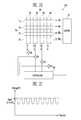
- FIGS. 1A and 1B are diagrams showing a touch screen panel 100 according to a first embodiment of the present invention.
- FIG. 1A illustrates the touch screen panel 100 in a noise measuring mode
- FIG. 1B illustrates the touch screen panel 100 in a touch recognizing mode.
- the touch screen panel 100 includes driving electrodes Tx, sensing electrodes Rx, a driver 10, and a controller 20.
- the driving electrodes Tx are formed along a first direction (e.g., an X-axis direction). In other embodiments, a plurality of driving electrodes may instead or in addition be arranged along a second direction (e.g., a Y-axis direction) that crosses the first direction.
- driving electrodes T1, T2, T3, and T4 have been illustrated in FIGS. 1A and 1B , but the number of driving electrodes may be different in other embodiments.
- the sensing electrodes Rx are arranged to cross the driving electrodes Tx. In the touch screen panel 100, the sensing electrodes Rx are formed along the second direction. In other embodiments, a plurality of sensing electrodes may instead or in addition be arranged along the first direction. Four sensing electrodes R1, R2, R3, and R4 have been illustrated in FIGS. 1A and 1B , but the number of sensing electrodes may be different in other embodiments.
- the driving and sensing electrodes Tx and Rx may be formed of a transparent conductive material.
- the driving and sensing electrodes Tx and Rx may be formed of indium tin oxide (ITO), indium zinc oxide (IZO), graphene, carbon nanotube, silver nanowires (AgNWs), or the like.
- ITO indium tin oxide
- IZO indium zinc oxide
- AgNWs silver nanowires
- the driving and sensing electrodes Tx and Rx are formed in a bar shape as shown in FIG. 1A .
- the shape of the driving and sensing electrodes Tx and Rx may be different in other embodiments.
- the driving and sensing electrodes Tx and Rx may be disposed on a substrate, such as a predetermined substrate.
- the substrate may be made of, for example, a material having insulation properties, such as glass, plastic, silicon, or synthetic resin.
- the substrate may be formed of metal or the like.
- the substrate may be implemented as a film having flexibility, which can be bent or folded.
- the driving and sensing electrodes Tx and Rx may be disposed in different layers from each other. To this end, an insulation layer may exist between the driving and sensing electrodes Tx and Rx. The insulation layer may partially exist only in a region in which the driving and sensing electrodes Tx and Rx cross each other.
- the driver 10 supplies a driving signal Ds to the driving electrodes Tx.
- the driver 10 may sequentially supply the driving signal Ds to the driving electrodes Tx.
- the touch recognizing mode is a mode in which a user's touch input to the touch screen panel 100 is detected.
- the driver 10 is controlled by the controller 20.
- the driver 10 may set the frequency of the driving signal Ds to avoid the frequency of a noise signal Ns detected by the controller 20.
- the controller 20 receives signals (for example, a touch signal Cs and the noise signal Ns) output from the sensing electrodes Rx. Accordingly, the controller 20 can detect a user's touch input in the touch recognizing mode, and can detect outside noise in the noise measuring mode.
- the noise measuring mode is a mode in which an outside noise signal (e.g., from an external environment) is detected.
- the outside noise signal may be detected when there is no user's touch being input to the touch screen panel 100.
- the noise measuring mode may be performed, for example, when the touch screen panel 100 is initially driven, and may again be performed during the operation of the touch screen panel 100.
- the noise measuring mode may be periodically performed to rapidly cope with a change in external environment.
- the controller 20 cuts off the electrical connection between at least one driving electrode Tx and the driver 10 to improve the reception sensitivity of external noise.
- the touch screen panel 100 further includes first switches S11, S12, S13, and S14 positioned between the respective driving electrodes Tx and the driver 10. The on/off operations of the first switches S11, S12, S13, and S14 are controlled by the controller 20.
- the controller 20 turns off at least one of the first switches S11, S12, S13, and S14 to cut off the electrical connection between a corresponding at least one driving electrode Tx and the driver 10.
- the controller 20 may detect the noise signal Ns output from the sensing electrodes Rx according to a change in capacitance caused by the outside noise.
- the first switches S11, S12, S13, and S14 are turned off to increase the reception sensitivity of this noise. Although four first switches S11, S12, S13, and S14 are illustrated in FIGS. 1A and 1B , the number of first switches may be different in other embodiments depending on factors such as the number of driving electrodes Tx.
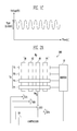
- FIG. 1C is a waveform diagram showing the noise signal Ns measured by the touch screen panel shown in FIG. 1A .
- the noise signal Ns is measured when the first switches S11, S12, S13, and S14 are turned off.
- the peak-to-peak voltage Vpp1 of the detected noise signal Ns was measured as 0.480V.
- the peak-to-peak voltage Vpp1 of the detected noise signal Ns is higher than the peak-to-peak voltage Vpp5 (0.250V, see FIG. 5B ) of a detected noise signal Ns measured in a comparable touch screen panel 500 of FIG. 5A .
- the reception sensitivity of noise when the electrical connection between the driving electrodes Tx and the driver 10 is cut off is higher than that of noise when the electrical connection between the driving electrodes Tx and the driver 10 is not cut off. This is because the outside noise sensed by the driving electrodes Tx does not come out to the driver 10 by cutting off the electrical connection between the driving electrodes Tx and the driver 10. Therefore, the reception sensitivity of the sensing electrodes Rx is increased.
- the controller 20 turns on the first switches S11, S12, S13, and S14 during the touch recognizing mode. Accordingly, the driving signal Ds supplied from the driver 10 is transmitted to the driving electrodes Tx. The controller 20 can then detect a user's touch by analyzing the touch signal Cs detected from the sensing electrodes Rx during the touch recognizing mode.
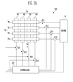
- FIGS. 2A and 2B are diagrams showing a touch screen panel 200 according to a second embodiment of the present invention.
- FIG. 2A illustrates the touch screen panel 200 in a noise measuring mode
- FIG. 2B illustrates the touch screen panel 200 in a touch recognizing mode.
- the touch screen panel 200 includes driving electrodes Tx, sensing electrodes Rx, a driver 10, and a controller 20.
- the driving electrodes Tx are formed along a first direction (e.g., an X-axis direction). In other embodiments, a plurality of driving electrodes may instead or in addition be arranged along a second direction (e.g., a Y-axis direction) that crosses the first direction.
- a first direction e.g., an X-axis direction
- a plurality of driving electrodes may instead or in addition be arranged along a second direction (e.g., a Y-axis direction) that crosses the first direction.
- Four driving electrodes T1, T2, T3, and T4 have been illustrated in FIGS. 2A and 2B , but the number of driving electrodes may be different in other embodiments.
- the sensing electrodes Rx are arranged to cross the driving electrodes Tx. In the touch screen panel 200, the sensing electrodes Rx are formed along the second direction. In other embodiments, a plurality of sensing electrodes may instead or in addition be arranged along the first direction. Four sensing electrodes R1, R2, R3, and R4 have been illustrated in FIGS. 2A and 2B , but the number of sensing electrodes may be different in other embodiments.
- the driving and sensing electrodes Tx and Rx may be formed of a transparent conductive material.
- the driving and sensing electrodes Tx and Rx may be formed of ITO, IZO, graphene, carbon nanotube, AgNWs, or the like.
- the driving and sensing electrodes Tx and Rx are formed in a bar shape as shown in FIG. 2A .
- the shape of the driving and sensing electrodes Tx and Rx may be different in other embodiments.
- the driving and sensing electrodes Tx and Rx may be disposed on a substrate, such as a predetermined substrate.
- the substrate may be made of, for example, a material having insulation properties, such as glass, plastic, silicon, or synthetic resin.
- the substrate may be formed of metal or the like.
- the substrate may be implemented as a film having flexibility, which can be bent or folded.
- the driving and sensing electrodes Tx and Rx may be disposed in different layers from each other. To this end, an insulation layer may exist between the driving and sensing electrodes Tx and Rx. The insulation layer may partially exist only in a region in which the driving and sensing electrodes Tx and Rx cross each other.
- the driver 10 supplies a driving signal Ds to the driving electrodes Tx.
- the driver 10 may sequentially supply the driving signal Ds to the driving electrodes Tx.
- the touch recognizing mode is a mode in which a user's touch input to the touch screen panel 200 is detected.
- the driver 10 is controlled by the controller 20.
- the driver 10 may set the frequency of the driving signal Ds to avoid the frequency of a noise signal Ns detected by the controller 20.
- the controller 20 receives signals (for example, a touch signal Cs and the noise signal Ns) output from the sensing electrodes Rx. Accordingly, the controller 20 can detect a user's touch input in the touch recognizing mode, and can detect outside noise in the noise measuring mode.
- the noise measuring mode is a mode in which an outside noise signal (e.g., from an external environment) is detected.
- the outside noise signal may be detected when there is no user's touch being input to the touch screen panel 200.
- the noise measuring mode may be performed, for example, when the touch screen panel 200 is initially driven, and may again be performed during the operation of the touch screen panel 200.
- the noise measuring mode may be periodically performed to rapidly cope with a change in external environment.
- the controller 20 cuts off the electrical connection between a portion of the sensing electrodes Rx and the controller 20 to improve the reception sensitivity of external noise.
- the touch screen panel 200 further includes second switches S21, S22, S23, and S24 positioned between the respective sensing electrodes Rx and the controller 20.
- the on/off operations of the second switches S21, S22, S23, and S24 are controlled by the controller 20.
- the controller 20 turns off a portion of the second switches S21, S22, S23, and S24 to cut off the electrical connection between a corresponding portion of the sensing electrodes Rx and the controller 20.
- the controller 20 may detect the noise signal Ns output from the sensing electrodes Rx according to a change in capacitance caused by the outside noise. For example, as shown in FIG. 2A , the controller 20 detects the noise signal Ns output from only one of the sensing electrodes Rx, in this case the third sensing electrode R3, by turning on only one of the second switches, namely, S23. The other second switches S21, S22, and S24 are turned off to increase the reception sensitivity of this noise. Although four second switches S21, S22, S23, and S24 are illustrated in FIGS. 2A and 2B , the number of second switches may be different in other embodiments depending on factors such as the number of sensing electrodes Rx.
- FIG. 2C is a waveform diagram showing the noise signal Ns measured by the touch screen panel shown in FIG. 2A .
- the noise signal Ns is measured when only one of the second switches S21, S22, S23, and S24 is turned on.
- the peak-to-peak voltage Vpp2 of the detected noise signal Ns was measured as 0.344V.
- the peak-to-peak voltage Vpp2 of the detected noise signal Ns is higher than the peak-to-peak voltage Vpp5 (0.250V, see FIG. 5B ) of the detected noise signal Ns measured in the comparable touch screen panel 500 of FIG. 5A .
- the reception sensitivity of noise when the electrical connection between a portion of the sensing electrodes Rx and the controller 20 is cut off is higher than that of noise when the electrical connection between the portion of the sensing electrodes Rx and the controller 20 is not cut off. This is because the outside noise sensed by the portion of the sensing electrodes Rx of which electrical connection to the controller 20 is cut off does not come out to the controller 20, but is instead concentrated on the sensing electrodes Rx that maintain the electrical connection to the controller 20.
- the controller 20 turns on the second switches S21, S22, S23, and S24 during the touch recognizing mode.
- the driver 10 transmits the driving signal Ds to the driving electrodes Tx during the touch recognizing mode.
- the controller 20 can detect a user's touch input by analyzing the touch signal Cs detected from the sensing electrodes Rx during the touch recognizing mode.
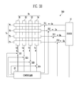
- FIGS. 3A and 3B are diagrams showing a touch screen panel 300 according to a third embodiment of the present invention.
- FIG. 3A illustrates the touch screen panel 300 in a noise measuring mode
- FIG. 3B illustrates the touch screen panel 300 in a touch recognizing mode.
- the touch screen panel 300 includes driving electrodes Tx, sensing electrodes Rx, a driver 10, and a controller 20.
- the driving electrodes Tx are formed along a first direction (e.g., an X-axis direction). In other embodiments, a plurality of driving electrodes may instead or in addition be arranged along a second direction (e.g., a Y-axis direction) that crosses the first direction.
- driving electrodes T1, T2, T3, and T4 have been illustrated in FIGS. 3A and 3B , but the number of driving electrodes may be different in other embodiments.
- the sensing electrodes Rx are arranged to cross the driving electrodes Tx. In the touch screen panel 100, the sensing electrodes Rx are formed along the second direction. In other embodiments, a plurality of sensing electrodes may instead or in addition be arranged along the first direction. Four sensing electrodes R1, R2, R3, and R4 have been illustrated in FIGS. 3A and 3B , but the number of sensing electrodes may be different in other embodiments.
- the driving and sensing electrodes Tx and Rx may be formed of a transparent conductive material.
- the driving and sensing electrodes Tx and Rx may be formed of ITO, IZO, graphene, carbon nanotube, AgNWs, or the like.
- the driving and sensing electrodes Tx and Rx are formed in a bar shape as shown in FIG. 3A .
- the shape of the driving and sensing electrodes Tx and Rx may be different in other embodiments.
- the driving and sensing electrodes Tx and Rx may be disposed on a substrate, such as a predetermined substrate.
- the substrate may be made of, for example, a material having insulation properties, such as glass, plastic, silicon, or synthetic resin.
- the substrate may be formed of metal or the like.
- the substrate may be implemented as a film having flexibility, which can be bent or folded.
- the driving and sensing electrodes Tx and Rx may be disposed in different layers from each other. To this end, an insulation layer may exist between the driving and sensing electrodes Tx and Rx. The insulation layer may partially exist only in a region in which the driving and sensing electrodes Tx and Rx cross each other.
- the driver 10 supplies a driving signal Ds to the driving electrodes Tx.
- the driver 10 may sequentially supply the driving signal Ds to the driving electrodes Tx.
- the touch recognizing mode is a mode in which a user's touch input to the touch screen panel 300 is detected.
- the driver 10 is controlled by the controller 20.
- the driver 10 may set the frequency of the driving signal Ds to avoid the frequency of a noise signal Ns detected by the controller 20.
- the controller 20 receives signals (for example, a touch signal Cs and the noise signal Ns) output from the sensing electrodes Rx. Accordingly, the controller 20 can detect a user's touch input in the touch recognizing mode, and can detect outside noise in the noise measuring mode.
- the noise measuring mode is a mode in which an outside noise signal (e.g., from an external environment) is detected. For example, the outside noise signal may be detected when there is no user's touch being input to the touch screen panel 300.
- the noise measuring mode may be performed, for example, when the touch screen panel 300 is initially driven, and may again be performed during the operation of the touch screen panel 300. For example, the noise measuring mode may be periodically performed to rapidly cope with a change in external environment.
- the controller 20 cuts off the electrical connection between at least one driving electrode Tx and the driver 10, and cuts off the electrical connection between a portion of the sensing electrodes Rx and the controller 20 to improve the reception sensitivity of external noise.
- the touch screen panel 300 further includes first switches S11, S12, S13, and S14 positioned between the respective driving electrodes Tx and the driver 10, and second switches S21, S22, S23, and S24 positioned between the respective sensing electrodes Rx and the controller 20.
- the on/off operations of the first switches S11, S12, S13, and S14 are controlled by the controller 20.
- the controller 20 turns off at least one of the first switches S11, S12, S13, and S14 to cut off the electrical connection between a corresponding at least one driving electrode Tx and the driver 10.
- four first switches S11, S12, S13, and S14 are illustrated in FIGS. 3A and 3B , the number of first switches may be different in other embodiments depending on factors such as the number of driving electrodes Tx.
- the second switches S21, S22, S23, and S24 are positioned between the respective sensing electrodes Rx and the controller 20.
- the on/off operations of the second switches S21, S22, S23, and S24 are controlled by the controller 20.
- the controller 20 turns off a portion of the second switches S21, S22, S23, and S24 to cut off the electrical connection between a corresponding portion of the sensing electrodes Rx and the controller 20.
- four second switches S21, S22, S23, and S24 are illustrated in FIGS. 3A and 3B , the number of second switches may be different in other embodiments depending on factors such as the number of sensing electrodes Rx.
- the controller 20 may detect the noise signal Ns output from the sensing electrodes Rx according to a change in capacitance caused by the outside noise. For example, as shown in FIG. 3A , the controller 20 detects the noise signal Ns output from only one of the sensing electrodes Rx, in this case the third sensing electrode R3.
- the first switches S11, S12, S13, and S14, and the other second switches S21, S22, and S24 are turned off to increase the reception sensitivity of this noise.
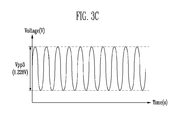
- FIG. 3C is a waveform diagram showing the noise signal Ns measured by the touch screen panel shown in FIG. 3A .
- the noise signal Ns is measured when the first switches S11, S12, S13, and S14 are turned off, and only one of the second switches S21, S22, S23, and S24 is turned on.
- the peak-to-peak voltage Vpp3 of the detected noise signal Ns was measured as 1.228V.
- the peak-to-peak voltage Vpp3 of the detected noise signal Ns is significantly higher than the peak-to-peak voltage Vpp5 (0.250V, see FIG. 5B ) of the detected noise signal Ns measured in the comparable touch screen panel 500 of FIG. 5A .
- the reception sensitivity of noise when the electrical connection between the driving electrodes Tx and the driver 10 is cut off, and the electrical connection between a portion of the sensing electrodes Rx and the controller 20 is cut off is significantly higher than that of noise when the electrical connection between the driving electrodes Tx and the driver 10 is not cut off, and the electrical connection between the portion of the sensing electrodes Rx and the controller 20 is not cut off.
- the outside noise sensed by the driving electrodes Tx does not come out to the driver 10 by cutting off the electrical connection between the driving electrodes Tx and the driver 10. Therefore, the reception sensitivity of the sensing electrodes Rx is increased.
- the outside noise sensed by the portion of the sensing electrodes Rx of which electrical connection to the controller 20 is cut off does not come out to the controller 20, but is instead concentrated on the sensing electrodes Rx that maintain the electrical connection to the controller 20.
- the controller 20 turns on the first switches S11, S12, S13, and S14, and the second switches S21, S22, S23, and S24 during the touch recognizing mode.
- the driver 10 transmits the driving signal Ds to the driving electrodes Tx during the touch recognizing mode.
- the controller 20 can detect a user's touch input by analyzing the touch signal Cs detected from the sensing electrodes Rx during the touch recognizing mode.
- FIGS. 4A and 4B are diagrams showing a touch screen panel 400 according to a fourth embodiment of the present invention.
- FIG. 4A illustrates the touch screen panel 400 in a noise measuring mode
- FIG. 4B illustrates the touch screen panel 400 in a touch recognizing mode.
- the touch screen panel 400 includes driving electrodes Tx, sensing electrodes Rx, a driver 10, and a controller 20.
- the driving electrodes Tx are formed along a first direction (e.g., an X-axis direction). In other embodiments, a plurality of driving electrodes may instead or in addition be arranged along a second direction (e.g., a Y-axis direction) that crosses the first direction.
- driving electrodes T1, T2, T3, and T4 have been illustrated in FIGS. 4A and 4B , but the number of driving electrodes may be different in other embodiments.
- the sensing electrodes Rx are arranged to cross the driving electrodes Tx. In the touch screen panel 400, the sensing electrodes Rx are formed along the second direction. In other embodiments, a plurality of sensing electrodes may instead or in addition be arranged along the first direction.
- Four sensing electrodes R1, R2, R3, and R4 have been illustrated in FIGS. 4A and 4B , but the number of sensing electrodes may be different in other embodiments.
- the driving and sensing electrodes Tx and Rx may be formed of a transparent conductive material.
- the driving and sensing electrodes Tx and Rx may be formed of ITO, IZO, graphene, carbon nanotube, AgNWs, or the like.
- the driving and sensing electrodes Tx and Rx are formed in a bar shape as shown in FIG. 4A .
- the shape of the driving and sensing electrodes Tx and Rx may be different in other embodiments.
- the driving and sensing electrodes Tx and Rx may be disposed on a substrate, such as a predetermined substrate.
- the substrate may be made of, for example, a material having insulation properties, such as glass, plastic, silicon, or synthetic resin.
- the substrate may be formed of metal or the like.
- the substrate may be implemented as a film having flexibility, which can be bent or folded.
- the driving and sensing electrodes Tx and Rx may be disposed in different layers from each other. To this end, an insulation layer may exist between the driving and sensing electrodes Tx and Rx. The insulation layer may partially exist only in a region in which the driving and sensing electrodes Tx and Rx cross each other.
- the driver supplies a driving signal Ds to the driving electrodes Tx.
- the driver 10 may sequentially supply the driving signal Ds to the driving electrodes Tx.
- the touch recognizing mode is a mode in which a user's touch input to the touch screen panel 400 is detected.
- the driver 10 is controlled by the controller 20.
- the driver 10 may set the frequency of the driving signal Ds to avoid the frequency of a noise signal Ns detected by the controller 20.
- the controller 20 receives signals (for example, a touch signal Cs and the noise signal Ns) output from the sensing electrodes Rx. Accordingly, the controller 20 can detect a user's touch input in the touch recognizing mode, and can detect noise input from the outside in the noise measuring mode.
- the noise measuring mode is a mode in which an outside noise signal (e.g., from an external environment) is detected.
- the noise signal may be detected when there is no user's touch being input to the touch screen panel 400.
- the noise measuring mode may be performed, for example, when the touch screen panel 400 is initially driven, and may again be performed during the operation of the touch screen panel 400.
- the noise measuring mode may be periodically performed to rapidly cope with a change in external environment.
- the controller 20 cuts off the electrical connection between at least one driving electrode Tx and the driver 10 to improve the reception sensitivity of external noise.
- the touch screen panel 400 further includes first switches S11, S12, S13, and S14 positioned between the respective driving electrodes Tx and the driver 10. The on/off operations of the first switches S11, S12, S13, and S14 are controlled by the controller 20.
- the controller 20 turns off at least one of the first switches S11, S12, S13, and S14 to cut off the electrical connection between a corresponding at least one driving electrode Tx and the driver 10.
- the controller 20 cuts off the electrical connection between a portion of the sensing electrodes Rx and the controller 20 to improve the reception sensitivity of external noise.
- the touch screen panel 400 further includes second switches S21, S22, S23, and S24 positioned between the respective sensing electrodes Rx and the controller 20. The on/off operations of the second switches S21, S22, S23, and S24 are controlled by the controller 20.
- the controller 20 turns off a portion of the second switches S21, S22, S23, and S24 to cut off the electrical connection between a corresponding portion of the sensing electrodes Rx and the controller 20.
- first switches S11, S12, S13, and S14 are illustrated in FIGS. 4A and 4B , the number of first switches may be different in other embodiments depending on factors such as the number of driving electrodes Tx.
- second switches S21, S22, S23, and S24 are illustrated in FIGS. 4A and 4B , the number of second switches may be different in other embodiments depending on factors such as the number of sensing electrodes Rx.
- the driving electrodes Tx and the sensing electrodes Rx are electrically connected to each other in the noise measuring mode.
- the touch screen panel 400 further includes a common line CL, third switches S31, S32, S33, and S34, and fourth switches S41, S42, S43, and S44.
- the third switches S31, S32, S33, and S34 are respectively positioned between the common line CL and common nodes N11, N12, N13, and N14, which are respectively positioned between the driving electrodes Tx and the first switches S11, S12, S13, and S14.
- the fourth switches S41, S42, S43, and S44 are respectively positioned between the common line CL and common nodes N21, N22, N23, and N24, which are respectively positioned between the sensing electrodes Rx and the second switches S21, S22, S23, and S24.
- the on/off operations of the third switches S31, S32, S33, and S34, and of the fourth switches S41, S42, S43, and S44 are controlled by the controller 20. Accordingly, when the third switches S31, S32, S33, and S34, and the fourth switches S41, S42, S43, and S44 are turned on, the driving and sensing electrodes Tx and Rx are electrically connected through the common line CL. Thus, the controller 20 turns on the third switches S31, S32, S33, and S34, and the fourth switches S41, S42, S43, and S44 during the noise measuring mode, so that the driving and sensing electrodes Tx and Rx are electrically connected to each other.
- the controller 20 may detect the noise signal Ns output from the sensing electrodes Rx according to a change in capacitance caused by the outside noise. For example, as shown in FIG. 4A , the controller 20 detects the noise signal Ns output from only one of the sensing electrodes Rx, in this case the third sensing electrode R3, by turning on only one of the second switches, namely, S23. To increase the reception sensitivity of this noise, the controller 20 turns off the first switches S11, S12, S13, and S14, and the other second switches S21, S22, and S24.
- FIG. 4C is a waveform diagram showing the noise signal Ns measured by the touch screen panel shown in FIG. 4A .
- the noise signal Ns is measured when the first switches S11, S12, S13, and S14 are turned off, only one of the second switches S21, S22, S23, and S24 is turned on, and the third switches S31, S32, S33, and S34, and the fourth switches S41, S42, S43, and S44 are turned on.
- the peak-to-peak voltage Vpp4 of the detected noise signal Ns was measured as 1.502V.
- the peak-to-peak voltage Vpp4 of the detected noise signal Ns is significantly higher than the peak-to-peak voltage Vpp5 (0.250V, see FIG. 5B ) of the detected noise signal Ns measured in the comparable touch screen panel 500 of FIG. 5A .
- the reception sensitivity of noise when the driving and sensing electrodes Tx and Rx are electrically connected to each other is significantly higher than that of noise when the driving and sensing electrodes Tx and Rx are not electrically connected to each other. This is because the driving and sensing electrodes Tx and Rx are electrically connected to each other, so that they behave as if they were one conductive plate. Accordingly, outside noise sensed by any of the driving and sensing electrodes Tx and Rx can be more easily detected by being concentrated on a specific sensing electrode Rx.
- the controller 20 turns on the first switches S11, S12, S13, and S14, and the second switches S21, S22, S23, and S24, and turns off the third switches S31, S32, S33, and S34, and the fourth switches S41, S42, S43, and S44 during the touch recognizing mode.
- the driver 10 transmits the driving signal Ds to the driving electrodes Tx during the touch recognizing mode. Accordingly, the controller 20 can detect a user's touch input by analyzing the touch signal Cs detected from the sensing electrodes Rx during the touch recognizing mode.
Landscapes
- Engineering & Computer Science (AREA)
- General Engineering & Computer Science (AREA)
- Theoretical Computer Science (AREA)
- Human Computer Interaction (AREA)
- Physics & Mathematics (AREA)
- General Physics & Mathematics (AREA)
- Computer Networks & Wireless Communication (AREA)
- Position Input By Displaying (AREA)
Applications Claiming Priority (1)
| Application Number | Priority Date | Filing Date | Title |
|---|---|---|---|
| KR1020120077783A KR101931737B1 (ko) | 2012-07-17 | 2012-07-17 | 터치 스크린 패널 및 그의 구동방법 |
Publications (3)
| Publication Number | Publication Date |
|---|---|
| EP2687960A2 true EP2687960A2 (fr) | 2014-01-22 |
| EP2687960A3 EP2687960A3 (fr) | 2014-11-12 |
| EP2687960B1 EP2687960B1 (fr) | 2016-12-14 |
Family
ID=47603463
Family Applications (1)
| Application Number | Title | Priority Date | Filing Date |
|---|---|---|---|
| EP13152776.4A Active EP2687960B1 (fr) | 2012-07-17 | 2013-01-25 | Panneau d'écran tactile et procédé de commande de celui-ci |
Country Status (6)
| Country | Link |
|---|---|
| US (1) | US9046944B2 (fr) |
| EP (1) | EP2687960B1 (fr) |
| JP (1) | JP6017234B2 (fr) |
| KR (1) | KR101931737B1 (fr) |
| CN (2) | CN103543870B (fr) |
| TW (1) | TWI612459B (fr) |
Cited By (2)
| Publication number | Priority date | Publication date | Assignee | Title |
|---|---|---|---|---|
| US10229307B2 (en) | 2016-06-17 | 2019-03-12 | Boe Technology Group Co., Ltd. | Detection circuit, method for recognizing structural features, and display substrate |
| GB2623544A (en) * | 2022-10-19 | 2024-04-24 | Touchnetix Ltd | Touch-sensitive apparatus and method |
Families Citing this family (28)
| Publication number | Priority date | Publication date | Assignee | Title |
|---|---|---|---|---|
| US9323398B2 (en) | 2009-07-10 | 2016-04-26 | Apple Inc. | Touch and hover sensing |
| WO2011075608A2 (fr) | 2009-12-18 | 2011-06-23 | Synaptics Incorporated | Dispositifs de détection transcapacitifs avec soudures ohmiques |
| US9851829B2 (en) | 2010-08-27 | 2017-12-26 | Apple Inc. | Signal processing for touch and hover sensing display device |
| US9201547B2 (en) | 2012-04-30 | 2015-12-01 | Apple Inc. | Wide dynamic range capacitive sensing |
| KR101931737B1 (ko) * | 2012-07-17 | 2018-12-26 | 삼성디스플레이 주식회사 | 터치 스크린 패널 및 그의 구동방법 |
| JP2015007924A (ja) | 2013-06-25 | 2015-01-15 | 株式会社ジャパンディスプレイ | タッチパネル付液晶表示装置 |
| JP2015072549A (ja) * | 2013-10-02 | 2015-04-16 | 株式会社ジャパンディスプレイ | タッチパネル付液晶表示装置 |
| CN103530012A (zh) * | 2013-10-31 | 2014-01-22 | 中环高科(天津)股份有限公司 | 一种采用单个触摸驱动模块驱动多个电容式触摸屏的方法 |
| US9746960B2 (en) | 2013-11-06 | 2017-08-29 | Apex Material Technology Corp. | Handling of electromagnetic interference in an electronic apparatus |
| TWI512569B (zh) * | 2013-11-06 | 2015-12-11 | Apex Material Technology Corp | 用於雜訊量測的觸控控制裝置、電子裝置及其方法 |
| US9933879B2 (en) * | 2013-11-25 | 2018-04-03 | Apple Inc. | Reconfigurable circuit topology for both self-capacitance and mutual capacitance sensing |
| US10725591B1 (en) | 2014-04-30 | 2020-07-28 | Cypress Semiconductor Corporation | Passive touch detection for capacitive sense array |
| CN104156129B (zh) * | 2014-07-11 | 2018-05-25 | 京东方科技集团股份有限公司 | 触控基板及显示装置 |
| KR102251775B1 (ko) | 2014-07-18 | 2021-05-12 | 삼성전자주식회사 | 전극 구조체 및 이를 사용하는 접촉 감지 센서 |
| KR102305323B1 (ko) * | 2014-09-10 | 2021-09-28 | 엘지디스플레이 주식회사 | 터치 센싱 장치 |
| US9619075B2 (en) * | 2014-12-09 | 2017-04-11 | Shenzhen China Star Optoelectronics Technology Co., Ltd | Embedded display panels and terminals with touch function, and touch detecting method |
| CN104484083B (zh) * | 2014-12-09 | 2018-07-17 | 深圳市华星光电技术有限公司 | 一种具有触摸功能的嵌入式显示屏、终端及触摸检测方法 |
| CN104503627B (zh) | 2015-01-14 | 2017-06-09 | 京东方科技集团股份有限公司 | 触控结构、触控显示面板和触控显示装置 |
| TWI594152B (zh) * | 2015-04-22 | 2017-08-01 | 友達光電股份有限公司 | 觸控偵測裝置 |
| EP3287938A4 (fr) | 2015-04-24 | 2018-12-26 | Shenzhen Goodix Technology Co., Ltd. | Circuit de détection de pixels pour l'identification d'empreintes digitales, système et dispositif électronique |
| CN104793829B (zh) * | 2015-05-08 | 2018-01-26 | 厦门天马微电子有限公司 | 一种触控装置、驱动方法、阵列基板和液晶显示面板 |
| US9874983B2 (en) * | 2015-06-23 | 2018-01-23 | Synaptics Incorporated | Electrode combining for noise determination |
| CN105095855B (zh) | 2015-06-26 | 2018-11-20 | 京东方科技集团股份有限公司 | 一种指纹识别器件、触控面板、输入设备及指纹识别方法 |
| KR102375274B1 (ko) * | 2015-09-10 | 2022-03-18 | 삼성디스플레이 주식회사 | 터치 감지 장치 및 이를 포함하는 표시 장치 |
| KR102593262B1 (ko) * | 2016-11-02 | 2023-10-26 | 삼성전자주식회사 | 터치 센서 컨트롤러 |
| KR20220085093A (ko) | 2020-12-14 | 2022-06-22 | 삼성디스플레이 주식회사 | 표시 장치 |
| USD1032267S1 (en) | 2021-12-09 | 2024-06-25 | Michael V. Halliday | Chair |
| US12436641B2 (en) * | 2022-07-29 | 2025-10-07 | Chongqing Boe Display Technology Co., Ltd. | Display panel having a touch structure and display apparatus |
Family Cites Families (23)
| Publication number | Priority date | Publication date | Assignee | Title |
|---|---|---|---|---|
| JP2603335Y2 (ja) * | 1992-02-28 | 2000-03-06 | グラフテック株式会社 | デジタイザ |
| US5565658A (en) * | 1992-07-13 | 1996-10-15 | Cirque Corporation | Capacitance-based proximity with interference rejection apparatus and methods |
| KR100202699B1 (ko) | 1996-03-26 | 1999-06-15 | 이종수 | 아날로그/매트릭스방식 겸용 터치판넬 |
| JP3436637B2 (ja) * | 1996-06-04 | 2003-08-11 | アルプス電気株式会社 | 座標入力装置 |
| WO2000044018A1 (fr) * | 1999-01-26 | 2000-07-27 | Harald Philipp | Capteur capacitif et montage |
| US7986193B2 (en) | 2007-01-03 | 2011-07-26 | Apple Inc. | Noise reduction within an electronic device using automatic frequency modulation |
| US9600124B2 (en) * | 2007-07-31 | 2017-03-21 | Atmel Corporation | Sensor and method of sensing |
| US8054090B2 (en) * | 2008-10-22 | 2011-11-08 | Atmel Corporation | Noise handling in capacitive touch sensors |
| US20100110040A1 (en) * | 2008-10-30 | 2010-05-06 | Samsung Electronics Co., Ltd. | Touch controller having increased sensing sensitivity, and display driving circuit and display device and system having the touch controller |
| TWI431520B (zh) * | 2009-08-14 | 2014-03-21 | Elan Microelectronics Corp | Front - end signal detectors and methods for improving the anti - noise capability of capacitive touch panels |
| WO2011050113A1 (fr) * | 2009-10-20 | 2011-04-28 | Cypress Semiconductor Corporation | Procédé et appareil de réduction de l'influence de bruit couplée dans des unités de commande d'écran tactile |
| KR101084426B1 (ko) | 2009-12-02 | 2011-11-21 | (주) 넥스트칩 | 동적 주파수 변조를 이용하는 터치 센서 칩 및 동작 방법 |
| KR20110091380A (ko) * | 2010-02-05 | 2011-08-11 | 삼성전자주식회사 | 터치 패널의 노이즈 보상 방법 및 장치 |
| JP5427648B2 (ja) | 2010-03-02 | 2014-02-26 | 株式会社ジャパンディスプレイ | 座標入力装置、およびそれを備えた表示装置 |
| JP4904410B2 (ja) * | 2010-04-14 | 2012-03-28 | パナソニック株式会社 | タッチパネル装置 |
| TW201200306A (en) * | 2010-06-17 | 2012-01-01 | Hou-Fei Hu | Dustproof structure of ratchet wrench |
| KR101182399B1 (ko) * | 2010-06-17 | 2012-09-12 | 주식회사 지니틱스 | 터치스크린 장치, 터치패널의 구동장치 및 구동방법 |
| KR101013514B1 (ko) | 2010-06-24 | 2011-02-10 | (주) 마스타 | 정전식 터치 패널 검사 장치 및 이를 이용한 검사 방법 |
| WO2012027005A1 (fr) * | 2010-08-23 | 2012-03-01 | Cypress Semiconductor Corporation | Circuits, procédés et systèmes de détection de capacité mutuelle |
| TW201210189A (en) * | 2010-08-25 | 2012-03-01 | Himax Tech Ltd | Filter for removing DC signal and high frequency noise and method thereof for touch sensor |
| JP5307110B2 (ja) * | 2010-12-01 | 2013-10-02 | 株式会社ジャパンディスプレイ | タッチパネル |
| CN102985835B (zh) * | 2011-07-15 | 2018-04-13 | 赛普拉斯半导体公司 | 具有接地插入电极的电容感测电路、方法和系统 |
| KR101931737B1 (ko) * | 2012-07-17 | 2018-12-26 | 삼성디스플레이 주식회사 | 터치 스크린 패널 및 그의 구동방법 |
-
2012
- 2012-07-17 KR KR1020120077783A patent/KR101931737B1/ko active Active
- 2012-09-13 JP JP2012201278A patent/JP6017234B2/ja active Active
- 2012-12-13 US US13/714,335 patent/US9046944B2/en active Active
-
2013
- 2013-01-23 TW TW102102446A patent/TWI612459B/zh active
- 2013-01-25 EP EP13152776.4A patent/EP2687960B1/fr active Active
- 2013-01-25 CN CN201310029648.7A patent/CN103543870B/zh active Active
- 2013-01-25 CN CN2013200413931U patent/CN203149513U/zh not_active Expired - Lifetime
Cited By (3)
| Publication number | Priority date | Publication date | Assignee | Title |
|---|---|---|---|---|
| US10229307B2 (en) | 2016-06-17 | 2019-03-12 | Boe Technology Group Co., Ltd. | Detection circuit, method for recognizing structural features, and display substrate |
| GB2623544A (en) * | 2022-10-19 | 2024-04-24 | Touchnetix Ltd | Touch-sensitive apparatus and method |
| GB2623544B (en) * | 2022-10-19 | 2025-06-25 | Touchnetix Ltd | Touch-sensitive apparatus and method |
Also Published As
| Publication number | Publication date |
|---|---|
| CN103543870B (zh) | 2018-07-10 |
| CN103543870A (zh) | 2014-01-29 |
| KR20140010797A (ko) | 2014-01-27 |
| TW201405404A (zh) | 2014-02-01 |
| EP2687960B1 (fr) | 2016-12-14 |
| US20140022188A1 (en) | 2014-01-23 |
| US9046944B2 (en) | 2015-06-02 |
| KR101931737B1 (ko) | 2018-12-26 |
| EP2687960A3 (fr) | 2014-11-12 |
| JP2014021963A (ja) | 2014-02-03 |
| JP6017234B2 (ja) | 2016-10-26 |
| CN203149513U (zh) | 2013-08-21 |
| TWI612459B (zh) | 2018-01-21 |
Similar Documents
| Publication | Publication Date | Title |
|---|---|---|
| EP2687960B1 (fr) | Panneau d'écran tactile et procédé de commande de celui-ci | |
| KR102228561B1 (ko) | 터치 센서를 포함하는 표시 장치 | |
| EP3048514B1 (fr) | Dispositif d'entrée tactile | |
| KR102257173B1 (ko) | 감소된 기생 커패시턴스를 위한 변조된 전력 공급부 | |
| US9779676B2 (en) | Integrated touch sensor and force sensor for an electronic device | |
| KR101410414B1 (ko) | 모션 감지 기능을 가지는 터치 스크린 패널 | |
| US9886144B2 (en) | Capacitive type touch sensor | |
| CN107817915A (zh) | 能触控感应基板 | |
| US10180761B2 (en) | Touch-panel-equipped display device including side surface electrodes | |
| US10809841B2 (en) | Method of human-machine interaction by combining touch and contactless controls | |
| US9471173B2 (en) | Capacitive input sensing in the presence of a uniform conductor | |
| CN105487734A (zh) | 电容触控式柔性显示面板及其柔性显示器 | |
| US20230280857A1 (en) | Touch sensing using polyvinylidene fluoride piezoelectric film | |
| KR102146585B1 (ko) | 송신기 전력 소비를 감소시키기 위한 시스템 및 방법 | |
| US10061445B2 (en) | Touch input device | |
| JP2016206790A (ja) | タッチ制御方法、タッチ制御装置、及びタッチ検出機能付き表示装置 | |
| KR20140086477A (ko) | 터치 감지 장치 | |
| US9354759B2 (en) | Touch screen panel | |
| US9977526B1 (en) | Display device with high touch detection sensitivity | |
| US20140028379A1 (en) | Single-layer capacitive touch-control panel apparatus | |
| US20150153869A1 (en) | Touchscreen device | |
| US20140184522A1 (en) | Touch-sensitive display panel | |
| US9519388B2 (en) | Touch sensor having multiple code matrices and driving method thereof | |
| US10191584B2 (en) | Reducing connections from a sensing module | |
| US20160092002A1 (en) | Touch sensing device |
Legal Events
| Date | Code | Title | Description |
|---|---|---|---|
| PUAI | Public reference made under article 153(3) epc to a published international application that has entered the european phase |
Free format text: ORIGINAL CODE: 0009012 |
|
| AK | Designated contracting states |
Kind code of ref document: A2 Designated state(s): AL AT BE BG CH CY CZ DE DK EE ES FI FR GB GR HR HU IE IS IT LI LT LU LV MC MK MT NL NO PL PT RO RS SE SI SK SM TR |
|
| AX | Request for extension of the european patent |
Extension state: BA ME |
|
| PUAL | Search report despatched |
Free format text: ORIGINAL CODE: 0009013 |
|
| AK | Designated contracting states |
Kind code of ref document: A3 Designated state(s): AL AT BE BG CH CY CZ DE DK EE ES FI FR GB GR HR HU IE IS IT LI LT LU LV MC MK MT NL NO PL PT RO RS SE SI SK SM TR |
|
| AX | Request for extension of the european patent |
Extension state: BA ME |
|
| RIC1 | Information provided on ipc code assigned before grant |
Ipc: G06F 3/041 20060101ALI20141003BHEP Ipc: G06F 3/044 20060101AFI20141003BHEP |
|
| 17P | Request for examination filed |
Effective date: 20150430 |
|
| RBV | Designated contracting states (corrected) |
Designated state(s): AL AT BE BG CH CY CZ DE DK EE ES FI FR GB GR HR HU IE IS IT LI LT LU LV MC MK MT NL NO PL PT RO RS SE SI SK SM TR |
|
| RAP1 | Party data changed (applicant data changed or rights of an application transferred) |
Owner name: SAMSUNG DISPLAY CO., LTD. |
|
| 17Q | First examination report despatched |
Effective date: 20150923 |
|
| GRAP | Despatch of communication of intention to grant a patent |
Free format text: ORIGINAL CODE: EPIDOSNIGR1 |
|
| INTG | Intention to grant announced |
Effective date: 20160622 |
|
| GRAS | Grant fee paid |
Free format text: ORIGINAL CODE: EPIDOSNIGR3 |
|
| STAA | Information on the status of an ep patent application or granted ep patent |
Free format text: STATUS: GRANT OF PATENT IS INTENDED |
|
| GRAA | (expected) grant |
Free format text: ORIGINAL CODE: 0009210 |
|
| STAA | Information on the status of an ep patent application or granted ep patent |
Free format text: STATUS: THE PATENT HAS BEEN GRANTED |
|
| AK | Designated contracting states |
Kind code of ref document: B1 Designated state(s): AL AT BE BG CH CY CZ DE DK EE ES FI FR GB GR HR HU IE IS IT LI LT LU LV MC MK MT NL NO PL PT RO RS SE SI SK SM TR |
|
| REG | Reference to a national code |
Ref country code: GB Ref legal event code: FG4D |
|
| REG | Reference to a national code |
Ref country code: CH Ref legal event code: EP |
|
| REG | Reference to a national code |
Ref country code: IE Ref legal event code: FG4D |
|
| REG | Reference to a national code |
Ref country code: AT Ref legal event code: REF Ref document number: 854151 Country of ref document: AT Kind code of ref document: T Effective date: 20170115 |
|
| REG | Reference to a national code |
Ref country code: DE Ref legal event code: R096 Ref document number: 602013015235 Country of ref document: DE |
|
| REG | Reference to a national code |
Ref country code: FR Ref legal event code: PLFP Year of fee payment: 5 |
|
| PG25 | Lapsed in a contracting state [announced via postgrant information from national office to epo] |
Ref country code: LV Free format text: LAPSE BECAUSE OF FAILURE TO SUBMIT A TRANSLATION OF THE DESCRIPTION OR TO PAY THE FEE WITHIN THE PRESCRIBED TIME-LIMIT Effective date: 20161214 |
|
| REG | Reference to a national code |
Ref country code: LT Ref legal event code: MG4D |
|
| REG | Reference to a national code |
Ref country code: NL Ref legal event code: MP Effective date: 20161214 |
|
| PG25 | Lapsed in a contracting state [announced via postgrant information from national office to epo] |
Ref country code: LT Free format text: LAPSE BECAUSE OF FAILURE TO SUBMIT A TRANSLATION OF THE DESCRIPTION OR TO PAY THE FEE WITHIN THE PRESCRIBED TIME-LIMIT Effective date: 20161214 Ref country code: GR Free format text: LAPSE BECAUSE OF FAILURE TO SUBMIT A TRANSLATION OF THE DESCRIPTION OR TO PAY THE FEE WITHIN THE PRESCRIBED TIME-LIMIT Effective date: 20170315 Ref country code: NO Free format text: LAPSE BECAUSE OF FAILURE TO SUBMIT A TRANSLATION OF THE DESCRIPTION OR TO PAY THE FEE WITHIN THE PRESCRIBED TIME-LIMIT Effective date: 20170314 Ref country code: SE Free format text: LAPSE BECAUSE OF FAILURE TO SUBMIT A TRANSLATION OF THE DESCRIPTION OR TO PAY THE FEE WITHIN THE PRESCRIBED TIME-LIMIT Effective date: 20161214 |
|
| REG | Reference to a national code |
Ref country code: AT Ref legal event code: MK05 Ref document number: 854151 Country of ref document: AT Kind code of ref document: T Effective date: 20161214 |
|
| PG25 | Lapsed in a contracting state [announced via postgrant information from national office to epo] |
Ref country code: BE Free format text: LAPSE BECAUSE OF NON-PAYMENT OF DUE FEES Effective date: 20170131 Ref country code: HR Free format text: LAPSE BECAUSE OF FAILURE TO SUBMIT A TRANSLATION OF THE DESCRIPTION OR TO PAY THE FEE WITHIN THE PRESCRIBED TIME-LIMIT Effective date: 20161214 Ref country code: RS Free format text: LAPSE BECAUSE OF FAILURE TO SUBMIT A TRANSLATION OF THE DESCRIPTION OR TO PAY THE FEE WITHIN THE PRESCRIBED TIME-LIMIT Effective date: 20161214 Ref country code: FI Free format text: LAPSE BECAUSE OF FAILURE TO SUBMIT A TRANSLATION OF THE DESCRIPTION OR TO PAY THE FEE WITHIN THE PRESCRIBED TIME-LIMIT Effective date: 20161214 |
|
| PG25 | Lapsed in a contracting state [announced via postgrant information from national office to epo] |
Ref country code: NL Free format text: LAPSE BECAUSE OF FAILURE TO SUBMIT A TRANSLATION OF THE DESCRIPTION OR TO PAY THE FEE WITHIN THE PRESCRIBED TIME-LIMIT Effective date: 20161214 |
|
| PG25 | Lapsed in a contracting state [announced via postgrant information from national office to epo] |
Ref country code: IS Free format text: LAPSE BECAUSE OF FAILURE TO SUBMIT A TRANSLATION OF THE DESCRIPTION OR TO PAY THE FEE WITHIN THE PRESCRIBED TIME-LIMIT Effective date: 20170414 Ref country code: RO Free format text: LAPSE BECAUSE OF FAILURE TO SUBMIT A TRANSLATION OF THE DESCRIPTION OR TO PAY THE FEE WITHIN THE PRESCRIBED TIME-LIMIT Effective date: 20161214 Ref country code: EE Free format text: LAPSE BECAUSE OF FAILURE TO SUBMIT A TRANSLATION OF THE DESCRIPTION OR TO PAY THE FEE WITHIN THE PRESCRIBED TIME-LIMIT Effective date: 20161214 Ref country code: CZ Free format text: LAPSE BECAUSE OF FAILURE TO SUBMIT A TRANSLATION OF THE DESCRIPTION OR TO PAY THE FEE WITHIN THE PRESCRIBED TIME-LIMIT Effective date: 20161214 Ref country code: SK Free format text: LAPSE BECAUSE OF FAILURE TO SUBMIT A TRANSLATION OF THE DESCRIPTION OR TO PAY THE FEE WITHIN THE PRESCRIBED TIME-LIMIT Effective date: 20161214 |
|
| PG25 | Lapsed in a contracting state [announced via postgrant information from national office to epo] |
Ref country code: AT Free format text: LAPSE BECAUSE OF FAILURE TO SUBMIT A TRANSLATION OF THE DESCRIPTION OR TO PAY THE FEE WITHIN THE PRESCRIBED TIME-LIMIT Effective date: 20161214 Ref country code: IT Free format text: LAPSE BECAUSE OF FAILURE TO SUBMIT A TRANSLATION OF THE DESCRIPTION OR TO PAY THE FEE WITHIN THE PRESCRIBED TIME-LIMIT Effective date: 20161214 Ref country code: ES Free format text: LAPSE BECAUSE OF FAILURE TO SUBMIT A TRANSLATION OF THE DESCRIPTION OR TO PAY THE FEE WITHIN THE PRESCRIBED TIME-LIMIT Effective date: 20161214 Ref country code: BE Free format text: LAPSE BECAUSE OF FAILURE TO SUBMIT A TRANSLATION OF THE DESCRIPTION OR TO PAY THE FEE WITHIN THE PRESCRIBED TIME-LIMIT Effective date: 20161214 Ref country code: SM Free format text: LAPSE BECAUSE OF FAILURE TO SUBMIT A TRANSLATION OF THE DESCRIPTION OR TO PAY THE FEE WITHIN THE PRESCRIBED TIME-LIMIT Effective date: 20161214 Ref country code: PT Free format text: LAPSE BECAUSE OF FAILURE TO SUBMIT A TRANSLATION OF THE DESCRIPTION OR TO PAY THE FEE WITHIN THE PRESCRIBED TIME-LIMIT Effective date: 20170414 Ref country code: BG Free format text: LAPSE BECAUSE OF FAILURE TO SUBMIT A TRANSLATION OF THE DESCRIPTION OR TO PAY THE FEE WITHIN THE PRESCRIBED TIME-LIMIT Effective date: 20170314 Ref country code: PL Free format text: LAPSE BECAUSE OF FAILURE TO SUBMIT A TRANSLATION OF THE DESCRIPTION OR TO PAY THE FEE WITHIN THE PRESCRIBED TIME-LIMIT Effective date: 20161214 |
|
| REG | Reference to a national code |
Ref country code: CH Ref legal event code: PL |
|
| REG | Reference to a national code |
Ref country code: DE Ref legal event code: R097 Ref document number: 602013015235 Country of ref document: DE |
|
| PG25 | Lapsed in a contracting state [announced via postgrant information from national office to epo] |
Ref country code: MC Free format text: LAPSE BECAUSE OF FAILURE TO SUBMIT A TRANSLATION OF THE DESCRIPTION OR TO PAY THE FEE WITHIN THE PRESCRIBED TIME-LIMIT Effective date: 20161214 |
|
| PLBE | No opposition filed within time limit |
Free format text: ORIGINAL CODE: 0009261 |
|
| STAA | Information on the status of an ep patent application or granted ep patent |
Free format text: STATUS: NO OPPOSITION FILED WITHIN TIME LIMIT |
|
| PG25 | Lapsed in a contracting state [announced via postgrant information from national office to epo] |
Ref country code: CH Free format text: LAPSE BECAUSE OF NON-PAYMENT OF DUE FEES Effective date: 20170131 Ref country code: LI Free format text: LAPSE BECAUSE OF NON-PAYMENT OF DUE FEES Effective date: 20170131 |
|
| REG | Reference to a national code |
Ref country code: IE Ref legal event code: MM4A |
|
| 26N | No opposition filed |
Effective date: 20170915 |
|
| PG25 | Lapsed in a contracting state [announced via postgrant information from national office to epo] |
Ref country code: LU Free format text: LAPSE BECAUSE OF NON-PAYMENT OF DUE FEES Effective date: 20170125 Ref country code: DK Free format text: LAPSE BECAUSE OF FAILURE TO SUBMIT A TRANSLATION OF THE DESCRIPTION OR TO PAY THE FEE WITHIN THE PRESCRIBED TIME-LIMIT Effective date: 20161214 |
|
| REG | Reference to a national code |
Ref country code: FR Ref legal event code: PLFP Year of fee payment: 6 |
|
| PG25 | Lapsed in a contracting state [announced via postgrant information from national office to epo] |
Ref country code: IE Free format text: LAPSE BECAUSE OF NON-PAYMENT OF DUE FEES Effective date: 20170125 Ref country code: SI Free format text: LAPSE BECAUSE OF FAILURE TO SUBMIT A TRANSLATION OF THE DESCRIPTION OR TO PAY THE FEE WITHIN THE PRESCRIBED TIME-LIMIT Effective date: 20161214 |
|
| PG25 | Lapsed in a contracting state [announced via postgrant information from national office to epo] |
Ref country code: MT Free format text: LAPSE BECAUSE OF NON-PAYMENT OF DUE FEES Effective date: 20170125 |
|
| PG25 | Lapsed in a contracting state [announced via postgrant information from national office to epo] |
Ref country code: HU Free format text: LAPSE BECAUSE OF FAILURE TO SUBMIT A TRANSLATION OF THE DESCRIPTION OR TO PAY THE FEE WITHIN THE PRESCRIBED TIME-LIMIT; INVALID AB INITIO Effective date: 20130125 |
|
| PG25 | Lapsed in a contracting state [announced via postgrant information from national office to epo] |
Ref country code: CY Free format text: LAPSE BECAUSE OF NON-PAYMENT OF DUE FEES Effective date: 20161214 |
|
| PG25 | Lapsed in a contracting state [announced via postgrant information from national office to epo] |
Ref country code: MK Free format text: LAPSE BECAUSE OF FAILURE TO SUBMIT A TRANSLATION OF THE DESCRIPTION OR TO PAY THE FEE WITHIN THE PRESCRIBED TIME-LIMIT Effective date: 20161214 |
|
| PG25 | Lapsed in a contracting state [announced via postgrant information from national office to epo] |
Ref country code: TR Free format text: LAPSE BECAUSE OF FAILURE TO SUBMIT A TRANSLATION OF THE DESCRIPTION OR TO PAY THE FEE WITHIN THE PRESCRIBED TIME-LIMIT Effective date: 20161214 |
|
| PG25 | Lapsed in a contracting state [announced via postgrant information from national office to epo] |
Ref country code: AL Free format text: LAPSE BECAUSE OF FAILURE TO SUBMIT A TRANSLATION OF THE DESCRIPTION OR TO PAY THE FEE WITHIN THE PRESCRIBED TIME-LIMIT Effective date: 20161214 |
|
| P01 | Opt-out of the competence of the unified patent court (upc) registered |
Effective date: 20230515 |
|
| PGFP | Annual fee paid to national office [announced via postgrant information from national office to epo] |
Ref country code: GB Payment date: 20251222 Year of fee payment: 14 |
|
| PGFP | Annual fee paid to national office [announced via postgrant information from national office to epo] |
Ref country code: FR Payment date: 20251223 Year of fee payment: 14 |
|
| PGFP | Annual fee paid to national office [announced via postgrant information from national office to epo] |
Ref country code: DE Payment date: 20251222 Year of fee payment: 14 |