EP2688190A2 - Convertisseur de tension à plusieurs niveaux - Google Patents
Convertisseur de tension à plusieurs niveaux Download PDFInfo
- Publication number
- EP2688190A2 EP2688190A2 EP12191958.3A EP12191958A EP2688190A2 EP 2688190 A2 EP2688190 A2 EP 2688190A2 EP 12191958 A EP12191958 A EP 12191958A EP 2688190 A2 EP2688190 A2 EP 2688190A2
- Authority
- EP
- European Patent Office
- Prior art keywords
- switch unit
- level voltage
- series
- switching devices
- switching
- Prior art date
- Legal status (The legal status is an assumption and is not a legal conclusion. Google has not performed a legal analysis and makes no representation as to the accuracy of the status listed.)
- Granted
Links
Images


Classifications
-
- H—ELECTRICITY
- H02—GENERATION; CONVERSION OR DISTRIBUTION OF ELECTRIC POWER
- H02M—APPARATUS FOR CONVERSION BETWEEN AC AND AC, BETWEEN AC AND DC, OR BETWEEN DC AND DC, AND FOR USE WITH MAINS OR SIMILAR POWER SUPPLY SYSTEMS; CONVERSION OF DC OR AC INPUT POWER INTO SURGE OUTPUT POWER; CONTROL OR REGULATION THEREOF
- H02M7/00—Conversion of AC power input into DC power output; Conversion of DC power input into AC power output
- H02M7/42—Conversion of DC power input into AC power output without possibility of reversal
- H02M7/44—Conversion of DC power input into AC power output without possibility of reversal by static converters
- H02M7/48—Conversion of DC power input into AC power output without possibility of reversal by static converters using discharge tubes with control electrode or semiconductor devices with control electrode
- H02M7/483—Converters with outputs that each can have more than two voltages levels
-
- H—ELECTRICITY
- H02—GENERATION; CONVERSION OR DISTRIBUTION OF ELECTRIC POWER
- H02M—APPARATUS FOR CONVERSION BETWEEN AC AND AC, BETWEEN AC AND DC, OR BETWEEN DC AND DC, AND FOR USE WITH MAINS OR SIMILAR POWER SUPPLY SYSTEMS; CONVERSION OF DC OR AC INPUT POWER INTO SURGE OUTPUT POWER; CONTROL OR REGULATION THEREOF
- H02M1/00—Details of apparatus for conversion
- H02M1/0095—Hybrid converter topologies, e.g. NPC mixed with flying capacitor, thyristor converter mixed with MMC or charge pump mixed with buck
-
- H—ELECTRICITY
- H02—GENERATION; CONVERSION OR DISTRIBUTION OF ELECTRIC POWER
- H02M—APPARATUS FOR CONVERSION BETWEEN AC AND AC, BETWEEN AC AND DC, OR BETWEEN DC AND DC, AND FOR USE WITH MAINS OR SIMILAR POWER SUPPLY SYSTEMS; CONVERSION OF DC OR AC INPUT POWER INTO SURGE OUTPUT POWER; CONTROL OR REGULATION THEREOF
- H02M7/00—Conversion of AC power input into DC power output; Conversion of DC power input into AC power output
- H02M7/42—Conversion of DC power input into AC power output without possibility of reversal
- H02M7/44—Conversion of DC power input into AC power output without possibility of reversal by static converters
- H02M7/48—Conversion of DC power input into AC power output without possibility of reversal by static converters using discharge tubes with control electrode or semiconductor devices with control electrode
- H02M7/483—Converters with outputs that each can have more than two voltages levels
- H02M7/4835—Converters with outputs that each can have more than two voltages levels comprising two or more cells, each including a switchable capacitor, the capacitors having a nominal charge voltage which corresponds to a given fraction of the input voltage, and the capacitors being selectively connected in series to determine the instantaneous output voltage
-
- H—ELECTRICITY
- H02—GENERATION; CONVERSION OR DISTRIBUTION OF ELECTRIC POWER
- H02M—APPARATUS FOR CONVERSION BETWEEN AC AND AC, BETWEEN AC AND DC, OR BETWEEN DC AND DC, AND FOR USE WITH MAINS OR SIMILAR POWER SUPPLY SYSTEMS; CONVERSION OF DC OR AC INPUT POWER INTO SURGE OUTPUT POWER; CONTROL OR REGULATION THEREOF
- H02M7/00—Conversion of AC power input into DC power output; Conversion of DC power input into AC power output
- H02M7/42—Conversion of DC power input into AC power output without possibility of reversal
- H02M7/44—Conversion of DC power input into AC power output without possibility of reversal by static converters
- H02M7/48—Conversion of DC power input into AC power output without possibility of reversal by static converters using discharge tubes with control electrode or semiconductor devices with control electrode
- H02M7/483—Converters with outputs that each can have more than two voltages levels
- H02M7/49—Combination of the output voltage waveforms of a plurality of converters
-
- H—ELECTRICITY
- H02—GENERATION; CONVERSION OR DISTRIBUTION OF ELECTRIC POWER
- H02M—APPARATUS FOR CONVERSION BETWEEN AC AND AC, BETWEEN AC AND DC, OR BETWEEN DC AND DC, AND FOR USE WITH MAINS OR SIMILAR POWER SUPPLY SYSTEMS; CONVERSION OF DC OR AC INPUT POWER INTO SURGE OUTPUT POWER; CONTROL OR REGULATION THEREOF
- H02M1/00—Details of apparatus for conversion
- H02M1/0067—Converter structures employing plural converter units, other than for parallel operation of the units on a single load
- H02M1/007—Plural converter units in cascade
-
- H—ELECTRICITY
- H02—GENERATION; CONVERSION OR DISTRIBUTION OF ELECTRIC POWER
- H02M—APPARATUS FOR CONVERSION BETWEEN AC AND AC, BETWEEN AC AND DC, OR BETWEEN DC AND DC, AND FOR USE WITH MAINS OR SIMILAR POWER SUPPLY SYSTEMS; CONVERSION OF DC OR AC INPUT POWER INTO SURGE OUTPUT POWER; CONTROL OR REGULATION THEREOF
- H02M1/00—Details of apparatus for conversion
- H02M1/08—Circuits specially adapted for the generation of control voltages for semiconductor devices incorporated in static converters
- H02M1/088—Circuits specially adapted for the generation of control voltages for semiconductor devices incorporated in static converters for the simultaneous control of series or parallel connected semiconductor devices
-
- H—ELECTRICITY
- H02—GENERATION; CONVERSION OR DISTRIBUTION OF ELECTRIC POWER
- H02M—APPARATUS FOR CONVERSION BETWEEN AC AND AC, BETWEEN AC AND DC, OR BETWEEN DC AND DC, AND FOR USE WITH MAINS OR SIMILAR POWER SUPPLY SYSTEMS; CONVERSION OF DC OR AC INPUT POWER INTO SURGE OUTPUT POWER; CONTROL OR REGULATION THEREOF
- H02M7/00—Conversion of AC power input into DC power output; Conversion of DC power input into AC power output
- H02M7/42—Conversion of DC power input into AC power output without possibility of reversal
- H02M7/44—Conversion of DC power input into AC power output without possibility of reversal by static converters
- H02M7/48—Conversion of DC power input into AC power output without possibility of reversal by static converters using discharge tubes with control electrode or semiconductor devices with control electrode
- H02M7/483—Converters with outputs that each can have more than two voltages levels
- H02M7/487—Neutral point clamped inverters
-
- Y—GENERAL TAGGING OF NEW TECHNOLOGICAL DEVELOPMENTS; GENERAL TAGGING OF CROSS-SECTIONAL TECHNOLOGIES SPANNING OVER SEVERAL SECTIONS OF THE IPC; TECHNICAL SUBJECTS COVERED BY FORMER USPC CROSS-REFERENCE ART COLLECTIONS [XRACs] AND DIGESTS
- Y02—TECHNOLOGIES OR APPLICATIONS FOR MITIGATION OR ADAPTATION AGAINST CLIMATE CHANGE
- Y02E—REDUCTION OF GREENHOUSE GAS [GHG] EMISSIONS, RELATED TO ENERGY GENERATION, TRANSMISSION OR DISTRIBUTION
- Y02E10/00—Energy generation through renewable energy sources
- Y02E10/70—Wind energy
- Y02E10/76—Power conversion electric or electronic aspects
Definitions
- the present disclosure relates to a converter. More particularly, the present disclosure relates to a multi-level voltage converter.
- a known method for achieving desired output voltage levels from a power conversion system is to utilize a multi-level power converter topology.
- Multi-level power converter topology has been used widely for power applications such as variable speed drive (VSD) systems, wind turbine generators, electric power distribution systems, etc. Power voltages with a higher number of voltage levels are applied to synthesize waveforms with a better harmonic spectrum. In other words, multi-level converters can reach desired voltage and minimize induced harmonics.
- VSD variable speed drive
- wind turbine generators wind turbine generators
- electric power distribution systems etc.
- Power voltages with a higher number of voltage levels are applied to synthesize waveforms with a better harmonic spectrum.
- multi-level converters can reach desired voltage and minimize induced harmonics.
- a typical multi-level converter has limits of outputting a power voltage with an increased number of voltage levels and is thus not easily controlled.
- increasing the number of converter levels also increases the control complexity and cost of converter circuits.
- An aspect of the present disclosure is related to a multi-level voltage converter.
- the multi-level voltage converter includes a multi-point converter circuit and at least one full bridge inverter circuit.
- the multi-point converter circuit is configured for converting a DC voltage into an intermediate multi-level voltage.
- the full bridge inverter circuit is electrically connected in series with the multi-point converter circuit and configured for receiving the intermediate multi-level voltage to generate a multi-level output voltage corresponding to a single phase output.
- the multi-level voltage converter includes a multi-point converter circuit and a plurality of cascade-connected full bridge inverter circuits.
- the multi-point converter circuit is configured for converting a DC voltage into an intermediate three-level voltage.
- the cascade-connected full bridge inverter circuits are electrically connected in series with the multi-point converter circuit and configured for receiving the intermediate three-level voltage to generate a (2 n+1 +1)-level output voltage corresponding to a single phase output, in which n is an amount of the cascade-connected full bridge inverter circuits.
- Coupled and “connected”, along with their derivatives, may be used.
- “connected” and “coupled” may be used to indicate that two or more elements are in direct physical or electrical contact with each other, or may also mean that two or more elements may be in indirect contact with each other.
- “Coupled” and “connected” may still be used to indicate that two or more elements cooperate or interact with each other.
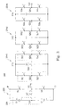
- Fig. 1 is a schematic diagram of a multi-level voltage converter according to one embodiment of the present disclosure.
- the multi-level voltage converter 100 includes at least one full bridge inverter circuit 110 and a multi-point converter circuit 120 (i.e., N-point converter circuit).
- the multi-point converter circuit 120 is configured for converting a DC voltage 2U into an intermediate multi-level voltage VL.
- the full bridge inverter circuit 110 is electrically connected in series with the multi-point converter circuit 120 to a single phase output and configured for receiving the intermediate multi-level voltage VL to generate a multi-level output voltage VP corresponding to the single phase output.
- the serial connection of the multi-point converter circuit with the full bridge inverter circuit in the present disclosure is merely illustrated for the single phase of the multi-level voltage converter.
- there may be three circuits (each of which can be configured as shown in Fig. 1 , or Fig. 2 or Fig. 3 shown below) electrically connected in parallel on a DC side to construct the multi-level voltage converter as a three-phase voltage converter.
- the full bridge inverter circuit 110 further includes a first switching pair 112, a second switching pair 114 and a voltage supporting device 116.
- the first switching pair 112 includes two switching devices S1 and S2 connected in series at a primary node Q1 between a positive node PS and a negative node NS.
- the second switching pair 114 includes two switching devices S3 and S4 connected in series between the positive node PS and the negative node NS at a secondary node Q2 configured for outputting the multi-level output voltage VP.
- the voltage supporting device 116 is electrically connected in parallel with the first switching pair 112 and the second switching pair 114 between the positive node PS and the negative node NS.
- the voltage supporting device 116 can be a capacitor, a DC voltage source, etc., which is able to maintain a DC voltage for a sufficient period of time
- each of the switching devices S1, S2, S3 and S4 can be implemented by a switch selected from the group consisting of an insulated gate bipolar transistor (IGBT), an integrated gate-commutated thyristor (IGCT), a power MOSFET, a bipolar junction transistor, etc., with an anti-parallel diode connected in parallel and reverse-biased with respect to the switch.
- each of the first switching pair 112 and the second switching pair 114 can be implemented by an IGBT module including two IGBTs and respective anti-parallel diodes connected in parallel thereto.
- the full bridge inverter circuit 110 can be designed and operated easily because its modular configuration provides flexibility for easy expansion of the number of levels without introducing undue complexity in the power circuit.
- the multi-point converter circuit 120 may further include a first switch unit 122, a second switch unit 124, an intermediate unit 126, and a third switch unit 128.
- the second switch unit 124 is electrically connected in series with the first switch unit 122 at an intermediate output terminal L, and the intermediate output terminal L is connected to the primary node Q1 of the full bridge inverter circuit 110 and configured for outputting the intermediate multi-level voltage VL, in which the first switch unit 122 is connected between the intermediate output terminal L and a positive DC terminal P, and the second switch unit 124 is connected between the intermediate output terminal L and a negative DC terminal N.
- the intermediate unit 126 includes two capacitors C1 and C2 electrically connected in series at a neutral point terminal NP between the positive DC terminal P and the negative DC terminal N, and in parallel with the serial connection of the first switch unit 122 and the second switch unit 124. Furthermore, the third switch unit 128 is electrically connected between the intermediate output terminal L and the neutral point terminal NP.
- the first switch unit 122 further includes a switching device S5
- the second switch unit 124 further includes a switching device S6, in which the switching device S5 and the switching device S6 are connected in series to the intermediate output terminal L between the positive DC terminal P and the negative DC terminal N.
- the third switch unit 128 may further include two switching devices S71 and S72 connected anti-serially (i.e., back-to-back connection) between the intermediate output terminal L and the neutral point terminal N P.
- the anti-serial connection of the switching devices S71 and S72 is configured for a current to flow back and forth between the intermediate output terminal L and the neutral point terminal NP.
- the first switch unit 122, the second switch unit 124 and the third switch unit 128 are arranged in parallel to each other between the intermediate output terminal L and the neutral point terminal NP, so that the configuration of the multi-point converter circuit 120 has three commutation paths between the intermediate output terminal L and the neutral point terminal NP, and each of the commutation paths is short and thus easily controlled.
- each of the switching devices S5, S6, S71 and S72 can be implemented by a switch selected from the group consisting of an IGBT, an IGCT, a power MOSFET, a bipolar junction transistor, etc., with an anti-parallel diode connected in parallel and reverse-biased with respect to the switch.
- each of the first switch unit 122, the second switch unit 124 and the third switch unit 128 can be implemented by an IGBT module as well.
- the multi-point converter circuit 120 can be operated to have multiple commutation paths between the intermediate output terminal L and the neutral point terminal NP, and each of the commutation paths is short and thus easily controlled. Furthermore, the configuration of the multi-point converter circuit 120 allows a modular design as well, and thus no complex circuitry is required such that the circuitry is simplified. In addition, the configuration of the multi-point converter circuit 120 simplifies the bus bar design since the switching loops (e.g., the loop formed from the neutral point terminal NP to the intermediate output terminal L) are simplified compared to the loops in a conventional multi-point converter circuit.
- the switching loops e.g., the loop formed from the neutral point terminal NP to the intermediate output terminal L
- the multi-point converter circuit 120 has three switching stages.
- the switching device S5 is turned on and the switching devices S6, S71, S72 are turned off, and the intermediate multi-level voltage VL becomes U.
- the switching devices S71, S72 are turned on and the switching devices S5, S6 are turned off, and the intermediate multi-level voltage VL is equal to zero.
- the switching device S6 is turned on while the switching devices S5, S71, S72 are turned off, and the intermediate multi-level voltage VL becomes -U.
- the multi-level output voltage VP has five voltage levels (i.e., U, U/2, 0, -U/2, -U) according to the operations of the multi-point converter circuit 120 and the full bridge inverter circuit 110.
- the multi-level output voltage VP becomes U
- the multi-level output voltage VP becomes U/2
- the multi-level output voltage VP is equal to zero
- the voltage levels -U/2 and -U may be deduced by analogy (for example, the operation in the condition of the switching device S6 being turned on).
- Fig. 2 is a schematic diagram of a multi-level voltage converter according to another embodiment of the present disclosure.
- the multi-level voltage converter 200 includes the full bridge inverter circuit 110 and a multi-point converter circuit 220, in which the connections and operations of the full bridge inverter circuit 110 and the multi-point converter circuit 220 are similar to those disclosed in Fig. 1 , and the connections of the first switch unit 222, the second switch unit 224, the intermediate unit 126, and the third switch unit 228 are similar to those disclosed in Fig. 1 as well.
- the first switch unit 222 further includes a plurality of switching devices (e.g., S51, S52, S53, S54) electrically connected in series to the intermediate output terminal L
- the second switch unit 224 further includes a plurality of switching devices (e.g., S61, S62, S63, S64) electrically connected in series to the intermediate output terminal L
- the third switch unit 228 further includes two groups of switching devices, which are connected anti-serially between the intermediate output terminal L and the neutral point terminal NP, in which each of the two groups includes a plurality of switching devices electrically connected in series (e.g., one group including switching devices S71, S72, and the other group including switching devices S73, S74).
- the switching devices S51, S52, S53, S54 are connected in series with the capacitor C1 between the intermediate output terminal L and the neutral point terminal NP to form a commutation path
- the switching devices S61, S62, S63, S64 are connected in series with the capacitor C2 between the intermediate output terminal L and the neutral point terminal NP to form another commutation path
- the group including the switching devices S71, S72 and the other group including the switching devices S73, S74 are connected anti-serially (i.e., back-to-back connection) between the intermediate output terminal L and the neutral point terminal NP to form still another commutation path and to be configured for a current to flow back and forth between the intermediate output terminal L and the neutral point terminal NP, thus resulting in each of the commutation paths being short and easily controlled.
- an amount of the series-connected switching devices in each of the first switch unit 222 and the second switch unit 224 can be increased to be any amount that is two times the amount of the series-connected switching devices in each of the two groups of switching devices in the third switch unit 228, in order to block the voltage which is two times the voltage across each of the switching devices S1, S2, S3 and S4.
- each of the switching devices S51-S54, S61-S64, S71-S74 can be implemented by a switch selected from the group consisting of an IGBT, an IGCT, a power MOSFET, a bipolar junction transistor, etc., with an anti-parallel diode connected in parallel and reverse-biased with respect to the switch.
- each of the first switch unit 222, the second switch unit 224 and the third switch unit 228 can be implemented by one or more IGBT modules as well.
- the operation of the multi-level voltage converter 200 is similar to that shown in Fig. 1 , and thus the operations would be understood by persons of ordinary skill in the art, so they are not described in further detail herein.
- Fig. 3 is a schematic diagram of a multi-level voltage converter according to yet another embodiment of the present disclosure.
- the multi-level voltage converter 300 includes a plurality of cascade-connected full bridge inverter circuits (i.e., full bridge inverter circuits 3101, 3102, ..., 310n) and a multi-point converter circuit 320.
- the multi-point converter circuit 120 is configured for converting a DC voltage (e.g., the voltage 2U) into the intermediate three-level voltage VL (e.g., the voltage VL with levels of U, 0, and -U).
- the cascade-connected full bridge inverter circuits 3101, 3102, ..., 310n are electrically connected in series with the multi-point converter circuit 320 to a single phase output and configured for receiving the intermediate three-level voltage VL to generate a (2 n+1 +1)-level output voltage VP corresponding to the single phase output, in which n is an amount of the cascade-connected full bridge inverter circuits.
- Each of the cascade-connected full bridge inverter circuits may further include a first switching pair 312, a second switching pair 314 and a voltage supporting device 316.
- the first switching pair 312 comprising two switch units S11 and S21 connected in series at a primary node (e.g., Q11).
- the second switching pair 314 includes two switching units S31 and S41 connected in series at a secondary node (e.g., Q21), in which the secondary node is connected to the primary node of a following full bridge inverter circuit (for example, the secondary node Q21 of the full bridge inverter circuit 3101 is connected to the primary node Q12 of the full bridge inverter circuit 3102).
- the voltage supporting device 316 is electrically connected in parallel with the first switching pair 312 and the second switching pair 314.
- the primary node of a first one of the cascade-connected full bridge inverter circuits i.e., the primary node Q11 of the full bridge inverter circuit 3101
- the secondary node of a last one of the cascade-connected full bridge inverter circuits i.e., the secondary node Q2n of the full bridge inverter circuit 310n
- the secondary node Q2n of the full bridge inverter circuit 310n is configured for outputting the (2 n+1 +1)-level output voltage.
- the amount of the full bridge inverter circuits can be increased according to practical needs, such that the number of voltage levels of the multi-level voltage converter 300 increases, and the waveform of output of the multi-level voltage converter 300 approaches a pure sine wave, thus resulting in lower harmonics in each output phase voltage.
- each of them correspondingly includes 2 (n-i) switching devices connected in series to the primary node or the secondary node, in order that the switch units S1 n, S2n, S3n and S4n is able to block the lowest voltage U/2 n in the multi-level voltage converter 300.
- the multi-point converter circuit 320 may further include a first switch unit S5, a second switch unit S6, an intermediate unit 326, and a third switch unit S7.
- the second switch unit S6 is electrically connected in series with the first switch unit S5 at the intermediate output terminal L, and the intermediate output terminal L is connected to the primary node of the first one of the cascade-connected full bridge inverter circuits, i.e., the primary node Q11 of the full bridge inverter circuit 3101, and configured for outputting the intermediate three-level voltage VL, in which the first switch unit S5 is connected between the intermediate output terminal L and the positive DC terminal P, and the second switch unit S6 is connected between the intermediate output terminal L and the negative DC terminal N.
- the intermediate unit 326 includes two capacitors C1 and C2 electrically connected in series at the neutral point terminal NP between the positive DC terminal P and the negative DC terminal N, and in parallel with the serial connection of the first switch unit S5 and the second switch unit S6. Furthermore, the third switch unit S7 is electrically connected between the intermediate output terminal L and the neutral point terminal NP.
- each of the first switch unit S5 and the second switch unit S6 may include a single switching device connected to the intermediate output terminal L, which is similar to that shown in the embodiment illustrated in Fig. 1 .
- the third switch unit S7 may further include two switching devices connected anti-serially between the intermediate output terminal L and the neutral point terminal NP, which is similar to that shown in the embodiment illustrated in Fig. 1 as well.
- each of the first switch unit S5 and the second switch unit S6 may further include a plurality of switching devices electrically connected in series to the intermediate output terminal VL, which is similar to that shown in the embodiment illustrated in Fig. 2 .
- the third switch unit S7 may further include two groups of switching devices, that are connected anti-serially between the intermediate output terminal VL and the neutral point terminal NP, in which each of the two groups includes a plurality of switching devices electrically connected in series, which is similar to that shown in the embodiment illustrated in Fig. 2 as well.
- an amount of the series-connected switching devices in each of the first switch unit S5 and the second switch unit S6 is 2 (n+1)
- an amount of the series-connected switching devices in each of the two groups of switching devices in the third switch unit S7 is 2 n , in order to block the voltage which is multiple times the voltage across each of the switching devices S1 n, S2n, S3n and S4n.
- each of the switch units S1 i, S2i, S3i, S4i, S5, S6, and S7 may include a corresponding number of switching devices according to practical needs.
- each of the switch units S12, S22, S32, S42 in the full bridge inverter circuit 3102 may include a single switching device
- each of the switch units S11, S21, S31, S41 in the full bridge inverter circuit 3101 may include two switching devices connected in series
- each of the first switch unit S5 and the second switch unit S6 in the multi-point converter circuit 320 may include eight switching devices connected in series
- each of two groups which are connected anti-serially in the third switch unit S7 may include four switching devices.
- each of the aforementioned switching device may be implemented by a switch selected from the group consisting of an IGBT, an IGCT, a power MOSFET, a bipolar junction transistor, etc., with an anti-parallel diode connected in parallel and reverse-biased with respect to the switch, and each of the aforementioned switch units can be implemented by one or more IGBT modules as well.
- the operation of the multi-level voltage converter 300 can be deduced by analogy to that shown in Fig. 1 , and thus the operations would be understood by persons of ordinary skill in the art, so they are not described in further detail herein.
- the multi-level voltage converter of the present disclosure not only can be easily configured to have a number of full bridge inverter circuits such that the number of voltage levels of the multi-level voltage converter increases and the waveform of output of the multi-level voltage converter approaches a pure sine wave, thus resulting in lower harmonics in each output phase voltage, but also can be configured to have multiple commutation paths by employing the multi-point converter circuit such that each of the commutation paths is short and thus easily controlled and the switching loops therein are simplified.
- the multi-point converter circuit and the full bridge inverter circuits can all have modular configurations, which provides flexibility for easy expansion of the number of levels without introducing undue complexity in the power circuit.
Landscapes
- Engineering & Computer Science (AREA)
- Power Engineering (AREA)
- Inverter Devices (AREA)
- Logic Circuits (AREA)
Applications Claiming Priority (1)
| Application Number | Priority Date | Filing Date | Title |
|---|---|---|---|
| US13/549,984 US8730696B2 (en) | 2012-07-16 | 2012-07-16 | Multi-level voltage converter |
Publications (3)
| Publication Number | Publication Date |
|---|---|
| EP2688190A2 true EP2688190A2 (fr) | 2014-01-22 |
| EP2688190A3 EP2688190A3 (fr) | 2018-03-14 |
| EP2688190B1 EP2688190B1 (fr) | 2019-10-02 |
Family
ID=47458639
Family Applications (1)
| Application Number | Title | Priority Date | Filing Date |
|---|---|---|---|
| EP12191958.3A Active EP2688190B1 (fr) | 2012-07-16 | 2012-11-09 | Convertisseur de tension à plusieurs niveaux |
Country Status (7)
| Country | Link |
|---|---|
| US (1) | US8730696B2 (fr) |
| EP (1) | EP2688190B1 (fr) |
| JP (1) | JP2014023420A (fr) |
| CN (1) | CN103546052B (fr) |
| BR (1) | BR102012033182A2 (fr) |
| ES (1) | ES2762218T3 (fr) |
| RU (1) | RU2584876C9 (fr) |
Cited By (1)
| Publication number | Priority date | Publication date | Assignee | Title |
|---|---|---|---|---|
| WO2019105550A1 (fr) * | 2017-11-30 | 2019-06-06 | Siemens Aktiengesellschaft | Sous-modules et dispositifs à sous-modules |
Families Citing this family (18)
| Publication number | Priority date | Publication date | Assignee | Title |
|---|---|---|---|---|
| US9099935B2 (en) * | 2013-01-14 | 2015-08-04 | Yaskawa America, Inc. | Single-phase active front end rectifier system for use with three-phase variable frequency drives |
| JP2015012621A (ja) * | 2013-06-26 | 2015-01-19 | 富士電機株式会社 | マルチレベル電力変換回路 |
| CN105703656A (zh) * | 2014-08-22 | 2016-06-22 | 特变电工新疆新能源股份有限公司 | 逆变单元及其控制方法、逆变器 |
| CN105656299B (zh) * | 2015-01-30 | 2018-10-30 | 华北电力大学 | 一种适用于全桥模块化多电平换流器的启动策略 |
| US10732685B2 (en) * | 2015-02-27 | 2020-08-04 | Ge Energy Power Conversion Technology Limited | System and method for operating power converters |
| US10191531B2 (en) * | 2015-12-29 | 2019-01-29 | General Electric Company | Hybrid converter system |
| CN107276378B (zh) * | 2016-04-08 | 2019-03-15 | 台达电子企业管理(上海)有限公司 | 预先充电控制方法 |
| CN105954610B (zh) * | 2016-04-26 | 2018-11-16 | 株洲中车时代电气股份有限公司 | 一种功率组件功率考核试验系统 |
| CN106169885B (zh) * | 2016-07-15 | 2019-02-12 | 华东交通大学 | 一种级联式六开关多电平逆变器 |
| US10536094B2 (en) | 2017-11-20 | 2020-01-14 | Solaredge Technologies Ltd. | Efficient switching for converter circuit |
| CN109361318B (zh) * | 2018-09-19 | 2021-03-02 | 上海交通大学 | 基于dab的单级隔离型pfc变换器直接电流控制系统及控制方法 |
| EP3709497B1 (fr) * | 2019-03-14 | 2022-12-28 | ABB Schweiz AG | Commande de convertisseur à modulation de largeur d'impulsion en cascade |
| CN111345889B (zh) * | 2020-03-30 | 2021-03-02 | 四川锦江电子科技有限公司 | 一种应用于脉冲电场消融技术的脉冲产生电路及控制方法 |
| US11601042B2 (en) * | 2020-05-14 | 2023-03-07 | Delta Electronics, Inc. | Multi-phase AC/DC converter |
| US10917021B1 (en) * | 2020-09-03 | 2021-02-09 | King Abdulaziz University | Multilevel inverter with reduced number of components |
| US12334814B2 (en) * | 2021-02-25 | 2025-06-17 | Mitsubishi Electric Corporation | Power converter |
| CN116707332B (zh) * | 2023-06-09 | 2024-02-02 | 深圳市恒运昌真空技术股份有限公司 | 一种逆变器及其多电平产生方法 |
| US20260106601A1 (en) * | 2024-10-16 | 2026-04-16 | Advanced Energy Industries, Inc. | Configurable fast transition pulse power supply unit |
Family Cites Families (21)
| Publication number | Priority date | Publication date | Assignee | Title |
|---|---|---|---|---|
| US5642275A (en) * | 1995-09-14 | 1997-06-24 | Lockheed Martin Energy System, Inc. | Multilevel cascade voltage source inverter with seperate DC sources |
| DE19720787A1 (de) * | 1997-05-17 | 1998-11-19 | Asea Brown Boveri | Verfahren zum Betrieb einer leistungselektronischen Schaltungsanordnung |
| JP2000166251A (ja) | 1998-12-01 | 2000-06-16 | Fuji Electric Co Ltd | 電力変換装置 |
| US6697271B2 (en) * | 2000-08-16 | 2004-02-24 | Northrop Grumman Corporation | Cascaded multi-level H-bridge drive |
| EP1253706B1 (fr) * | 2001-04-25 | 2013-08-07 | ABB Schweiz AG | Circuit d'électronique de puissane et procédé pour transférer la puissance active |
| DE10131961A1 (de) * | 2001-07-02 | 2003-01-23 | Siemens Ag | N-Punkt-Stromrichterschaltung |
| US6969967B2 (en) * | 2003-12-12 | 2005-11-29 | Ut-Battelle Llc | Multi-level dc bus inverter for providing sinusoidal and PWM electrical machine voltages |
| RU2269196C1 (ru) * | 2004-07-20 | 2006-01-27 | Государственное унитарное предприятие "Всероссийский электротехнический институт им. В.И. Ленина" | Преобразователь напряжения, выполненный по комбинированной схеме |
| JP2006101668A (ja) * | 2004-09-30 | 2006-04-13 | Honda Motor Co Ltd | 電源装置 |
| JP5019823B2 (ja) | 2006-08-16 | 2012-09-05 | 三菱電機株式会社 | 無効電力補償装置 |
| EP3046251B1 (fr) * | 2007-07-09 | 2018-06-06 | Power Concepts NZ Limited | Convertisseur multisortie |
| US7839023B2 (en) * | 2007-07-18 | 2010-11-23 | Raytheon Company | Methods and apparatus for three-phase inverter with reduced energy storage |
| UA37698U (ru) * | 2008-05-22 | 2008-12-10 | Государственное Высшее Учебное Заведение "Донецкий Национальный Технический Университет" | Гибридный несимметричный многоуровневый преобразователь частоты |
| EP2357721B1 (fr) * | 2008-11-18 | 2016-03-30 | Mitsubishi Electric Corporation | Dispositif de conversion de courant |
| CN101494425A (zh) * | 2009-01-19 | 2009-07-29 | 上海海事大学 | 三相混合多电平逆变电路 |
| EP2383877B1 (fr) * | 2009-01-29 | 2018-09-05 | Mitsubishi Electric Corporation | Dispositif de conversion de puissance |
| CA2757750C (fr) * | 2009-04-09 | 2016-07-26 | Abb Schweiz Ag | Agencement d'echange d'energie |
| CN101572503A (zh) * | 2009-06-01 | 2009-11-04 | 浙江大学 | 通用型开关电容二极管箝位组合多电平电路 |
| JP5457449B2 (ja) * | 2009-06-19 | 2014-04-02 | 三菱電機株式会社 | 電力変換装置 |
| US8144490B2 (en) * | 2009-11-10 | 2012-03-27 | General Electric Company | Operation of a three level converter |
| RU2411627C1 (ru) * | 2010-01-11 | 2011-02-10 | Открытое акционерное общество "Всероссийский научно-исследовательский проектно-конструкторский и технологический институт релестроения с опытным производством" | Многоуровневый автономный инвертор напряжения |
-
2012
- 2012-07-16 US US13/549,984 patent/US8730696B2/en active Active
- 2012-10-01 RU RU2012141658A patent/RU2584876C9/ru active
- 2012-10-23 JP JP2012234114A patent/JP2014023420A/ja active Pending
- 2012-10-25 CN CN201210413180.7A patent/CN103546052B/zh active Active
- 2012-11-09 ES ES12191958T patent/ES2762218T3/es active Active
- 2012-11-09 EP EP12191958.3A patent/EP2688190B1/fr active Active
- 2012-12-26 BR BR102012033182-9A patent/BR102012033182A2/pt not_active IP Right Cessation
Non-Patent Citations (1)
| Title |
|---|
| None |
Cited By (1)
| Publication number | Priority date | Publication date | Assignee | Title |
|---|---|---|---|---|
| WO2019105550A1 (fr) * | 2017-11-30 | 2019-06-06 | Siemens Aktiengesellschaft | Sous-modules et dispositifs à sous-modules |
Also Published As
| Publication number | Publication date |
|---|---|
| BR102012033182A2 (pt) | 2014-05-06 |
| US20140016380A1 (en) | 2014-01-16 |
| US8730696B2 (en) | 2014-05-20 |
| EP2688190A3 (fr) | 2018-03-14 |
| ES2762218T3 (es) | 2020-05-22 |
| RU2584876C9 (ru) | 2017-03-20 |
| JP2014023420A (ja) | 2014-02-03 |
| CN103546052B (zh) | 2016-03-16 |
| RU2584876C2 (ru) | 2016-05-20 |
| RU2012141658A (ru) | 2014-04-10 |
| CN103546052A (zh) | 2014-01-29 |
| EP2688190B1 (fr) | 2019-10-02 |
Similar Documents
| Publication | Publication Date | Title |
|---|---|---|
| EP2688190B1 (fr) | Convertisseur de tension à plusieurs niveaux | |
| US8934268B2 (en) | Power electronic converter for use in high voltage direct current power transmission | |
| US8837176B2 (en) | Converter with reactive power compensation | |
| Farhadi Kangarlu et al. | Symmetric multilevel inverter with reduced components based on non-insulated dc voltage sources | |
| US9641098B2 (en) | Multi-level inverter apparatus and method | |
| US20160218637A1 (en) | A new four-level converter cell topology for cascaded modular multilevel converters | |
| US20150003134A1 (en) | Modular multilevel converter using asymmetry | |
| US9344010B2 (en) | Power electronic converter | |
| US20130088901A1 (en) | Multilevel inverter | |
| CA2587421C (fr) | Circuit convertisseur pour la commutation d'une multiplicite de niveaux de tensions de commutation | |
| US20160352239A1 (en) | Power electronic converter | |
| WO2017089365A1 (fr) | Convertisseur de puissance à quatre niveaux | |
| Hajirayat et al. | A novel nested T-type four-level inverter for medium voltage applications | |
| WO2016105272A1 (fr) | Circuit d'équilibrage et onduleur le comprenant | |
| Hosseinzadeh et al. | New single-phase asymmetric reduced multilevel inverter based on switched-diode for cascaded multilevel inverters | |
| Kumar et al. | A new switching scheme for fuel cell supported reduced switch three-phase multilevel inverter topology | |
| Fatima et al. | Design of New Cascaded Multilevel Inverter with Symmetrical DC-voltage Source | |
| Liu et al. | Optimal Modulation Algorithm for Hybrid Clamped Three-Level Inverter |
Legal Events
| Date | Code | Title | Description |
|---|---|---|---|
| PUAI | Public reference made under article 153(3) epc to a published international application that has entered the european phase |
Free format text: ORIGINAL CODE: 0009012 |
|
| AK | Designated contracting states |
Kind code of ref document: A2 Designated state(s): AL AT BE BG CH CY CZ DE DK EE ES FI FR GB GR HR HU IE IS IT LI LT LU LV MC MK MT NL NO PL PT RO RS SE SI SK SM TR |
|
| AX | Request for extension of the european patent |
Extension state: BA ME |
|
| PUAL | Search report despatched |
Free format text: ORIGINAL CODE: 0009013 |
|
| AK | Designated contracting states |
Kind code of ref document: A3 Designated state(s): AL AT BE BG CH CY CZ DE DK EE ES FI FR GB GR HR HU IE IS IT LI LT LU LV MC MK MT NL NO PL PT RO RS SE SI SK SM TR |
|
| AX | Request for extension of the european patent |
Extension state: BA ME |
|
| RIC1 | Information provided on ipc code assigned before grant |
Ipc: H02M 7/487 20070101ALI20180206BHEP Ipc: H02M 7/49 20070101ALI20180206BHEP Ipc: H02M 7/483 20070101AFI20180206BHEP |
|
| STAA | Information on the status of an ep patent application or granted ep patent |
Free format text: STATUS: REQUEST FOR EXAMINATION WAS MADE |
|
| 17P | Request for examination filed |
Effective date: 20180912 |
|
| RBV | Designated contracting states (corrected) |
Designated state(s): AL AT BE BG CH CY CZ DE DK EE ES FI FR GB GR HR HU IE IS IT LI LT LU LV MC MK MT NL NO PL PT RO RS SE SI SK SM TR |
|
| STAA | Information on the status of an ep patent application or granted ep patent |
Free format text: STATUS: EXAMINATION IS IN PROGRESS |
|
| 17Q | First examination report despatched |
Effective date: 20181030 |
|
| GRAP | Despatch of communication of intention to grant a patent |
Free format text: ORIGINAL CODE: EPIDOSNIGR1 |
|
| STAA | Information on the status of an ep patent application or granted ep patent |
Free format text: STATUS: GRANT OF PATENT IS INTENDED |
|
| INTG | Intention to grant announced |
Effective date: 20190417 |
|
| GRAS | Grant fee paid |
Free format text: ORIGINAL CODE: EPIDOSNIGR3 |
|
| GRAA | (expected) grant |
Free format text: ORIGINAL CODE: 0009210 |
|
| STAA | Information on the status of an ep patent application or granted ep patent |
Free format text: STATUS: THE PATENT HAS BEEN GRANTED |
|
| AK | Designated contracting states |
Kind code of ref document: B1 Designated state(s): AL AT BE BG CH CY CZ DE DK EE ES FI FR GB GR HR HU IE IS IT LI LT LU LV MC MK MT NL NO PL PT RO RS SE SI SK SM TR |
|
| REG | Reference to a national code |
Ref country code: GB Ref legal event code: FG4D |
|
| REG | Reference to a national code |
Ref country code: CH Ref legal event code: EP Ref country code: AT Ref legal event code: REF Ref document number: 1187321 Country of ref document: AT Kind code of ref document: T Effective date: 20191015 |
|
| REG | Reference to a national code |
Ref country code: DE Ref legal event code: R096 Ref document number: 602012064478 Country of ref document: DE |
|
| REG | Reference to a national code |
Ref country code: IE Ref legal event code: FG4D |
|
| REG | Reference to a national code |
Ref country code: DE Ref legal event code: R082 Ref document number: 602012064478 Country of ref document: DE Representative=s name: DF-MP DOERRIES FRANK-MOLNIA & POHLMAN PATENTAN, DE |
|
| REG | Reference to a national code |
Ref country code: NL Ref legal event code: FP |
|
| REG | Reference to a national code |
Ref country code: LT Ref legal event code: MG4D |
|
| REG | Reference to a national code |
Ref country code: AT Ref legal event code: MK05 Ref document number: 1187321 Country of ref document: AT Kind code of ref document: T Effective date: 20191002 |
|
| PG25 | Lapsed in a contracting state [announced via postgrant information from national office to epo] |
Ref country code: PL Free format text: LAPSE BECAUSE OF FAILURE TO SUBMIT A TRANSLATION OF THE DESCRIPTION OR TO PAY THE FEE WITHIN THE PRESCRIBED TIME-LIMIT Effective date: 20191002 Ref country code: SE Free format text: LAPSE BECAUSE OF FAILURE TO SUBMIT A TRANSLATION OF THE DESCRIPTION OR TO PAY THE FEE WITHIN THE PRESCRIBED TIME-LIMIT Effective date: 20191002 Ref country code: BG Free format text: LAPSE BECAUSE OF FAILURE TO SUBMIT A TRANSLATION OF THE DESCRIPTION OR TO PAY THE FEE WITHIN THE PRESCRIBED TIME-LIMIT Effective date: 20200102 Ref country code: LT Free format text: LAPSE BECAUSE OF FAILURE TO SUBMIT A TRANSLATION OF THE DESCRIPTION OR TO PAY THE FEE WITHIN THE PRESCRIBED TIME-LIMIT Effective date: 20191002 Ref country code: FI Free format text: LAPSE BECAUSE OF FAILURE TO SUBMIT A TRANSLATION OF THE DESCRIPTION OR TO PAY THE FEE WITHIN THE PRESCRIBED TIME-LIMIT Effective date: 20191002 Ref country code: LV Free format text: LAPSE BECAUSE OF FAILURE TO SUBMIT A TRANSLATION OF THE DESCRIPTION OR TO PAY THE FEE WITHIN THE PRESCRIBED TIME-LIMIT Effective date: 20191002 Ref country code: NO Free format text: LAPSE BECAUSE OF FAILURE TO SUBMIT A TRANSLATION OF THE DESCRIPTION OR TO PAY THE FEE WITHIN THE PRESCRIBED TIME-LIMIT Effective date: 20200102 Ref country code: GR Free format text: LAPSE BECAUSE OF FAILURE TO SUBMIT A TRANSLATION OF THE DESCRIPTION OR TO PAY THE FEE WITHIN THE PRESCRIBED TIME-LIMIT Effective date: 20200103 Ref country code: PT Free format text: LAPSE BECAUSE OF FAILURE TO SUBMIT A TRANSLATION OF THE DESCRIPTION OR TO PAY THE FEE WITHIN THE PRESCRIBED TIME-LIMIT Effective date: 20200203 Ref country code: AT Free format text: LAPSE BECAUSE OF FAILURE TO SUBMIT A TRANSLATION OF THE DESCRIPTION OR TO PAY THE FEE WITHIN THE PRESCRIBED TIME-LIMIT Effective date: 20191002 |
|
| REG | Reference to a national code |
Ref country code: ES Ref legal event code: FG2A Ref document number: 2762218 Country of ref document: ES Kind code of ref document: T3 Effective date: 20200522 |
|
| PG25 | Lapsed in a contracting state [announced via postgrant information from national office to epo] |
Ref country code: RS Free format text: LAPSE BECAUSE OF FAILURE TO SUBMIT A TRANSLATION OF THE DESCRIPTION OR TO PAY THE FEE WITHIN THE PRESCRIBED TIME-LIMIT Effective date: 20191002 Ref country code: CZ Free format text: LAPSE BECAUSE OF FAILURE TO SUBMIT A TRANSLATION OF THE DESCRIPTION OR TO PAY THE FEE WITHIN THE PRESCRIBED TIME-LIMIT Effective date: 20191002 Ref country code: IS Free format text: LAPSE BECAUSE OF FAILURE TO SUBMIT A TRANSLATION OF THE DESCRIPTION OR TO PAY THE FEE WITHIN THE PRESCRIBED TIME-LIMIT Effective date: 20200224 Ref country code: HR Free format text: LAPSE BECAUSE OF FAILURE TO SUBMIT A TRANSLATION OF THE DESCRIPTION OR TO PAY THE FEE WITHIN THE PRESCRIBED TIME-LIMIT Effective date: 20191002 |
|
| PG25 | Lapsed in a contracting state [announced via postgrant information from national office to epo] |
Ref country code: AL Free format text: LAPSE BECAUSE OF FAILURE TO SUBMIT A TRANSLATION OF THE DESCRIPTION OR TO PAY THE FEE WITHIN THE PRESCRIBED TIME-LIMIT Effective date: 20191002 |
|
| REG | Reference to a national code |
Ref country code: CH Ref legal event code: PL |
|
| REG | Reference to a national code |
Ref country code: DE Ref legal event code: R097 Ref document number: 602012064478 Country of ref document: DE |
|
| PG2D | Information on lapse in contracting state deleted |
Ref country code: IS |
|
| PG25 | Lapsed in a contracting state [announced via postgrant information from national office to epo] |
Ref country code: MC Free format text: LAPSE BECAUSE OF FAILURE TO SUBMIT A TRANSLATION OF THE DESCRIPTION OR TO PAY THE FEE WITHIN THE PRESCRIBED TIME-LIMIT Effective date: 20191002 Ref country code: LU Free format text: LAPSE BECAUSE OF NON-PAYMENT OF DUE FEES Effective date: 20191109 Ref country code: DK Free format text: LAPSE BECAUSE OF FAILURE TO SUBMIT A TRANSLATION OF THE DESCRIPTION OR TO PAY THE FEE WITHIN THE PRESCRIBED TIME-LIMIT Effective date: 20191002 Ref country code: EE Free format text: LAPSE BECAUSE OF FAILURE TO SUBMIT A TRANSLATION OF THE DESCRIPTION OR TO PAY THE FEE WITHIN THE PRESCRIBED TIME-LIMIT Effective date: 20191002 Ref country code: RO Free format text: LAPSE BECAUSE OF FAILURE TO SUBMIT A TRANSLATION OF THE DESCRIPTION OR TO PAY THE FEE WITHIN THE PRESCRIBED TIME-LIMIT Effective date: 20191002 Ref country code: CH Free format text: LAPSE BECAUSE OF NON-PAYMENT OF DUE FEES Effective date: 20191130 Ref country code: LI Free format text: LAPSE BECAUSE OF NON-PAYMENT OF DUE FEES Effective date: 20191130 Ref country code: IS Free format text: LAPSE BECAUSE OF FAILURE TO SUBMIT A TRANSLATION OF THE DESCRIPTION OR TO PAY THE FEE WITHIN THE PRESCRIBED TIME-LIMIT Effective date: 20200202 |
|
| PLBE | No opposition filed within time limit |
Free format text: ORIGINAL CODE: 0009261 |
|
| STAA | Information on the status of an ep patent application or granted ep patent |
Free format text: STATUS: NO OPPOSITION FILED WITHIN TIME LIMIT |
|
| REG | Reference to a national code |
Ref country code: BE Ref legal event code: MM Effective date: 20191130 |
|
| PG25 | Lapsed in a contracting state [announced via postgrant information from national office to epo] |
Ref country code: SK Free format text: LAPSE BECAUSE OF FAILURE TO SUBMIT A TRANSLATION OF THE DESCRIPTION OR TO PAY THE FEE WITHIN THE PRESCRIBED TIME-LIMIT Effective date: 20191002 Ref country code: SM Free format text: LAPSE BECAUSE OF FAILURE TO SUBMIT A TRANSLATION OF THE DESCRIPTION OR TO PAY THE FEE WITHIN THE PRESCRIBED TIME-LIMIT Effective date: 20191002 |
|
| 26N | No opposition filed |
Effective date: 20200703 |
|
| PG25 | Lapsed in a contracting state [announced via postgrant information from national office to epo] |
Ref country code: IE Free format text: LAPSE BECAUSE OF NON-PAYMENT OF DUE FEES Effective date: 20191109 |
|
| PG25 | Lapsed in a contracting state [announced via postgrant information from national office to epo] |
Ref country code: BE Free format text: LAPSE BECAUSE OF NON-PAYMENT OF DUE FEES Effective date: 20191130 Ref country code: SI Free format text: LAPSE BECAUSE OF FAILURE TO SUBMIT A TRANSLATION OF THE DESCRIPTION OR TO PAY THE FEE WITHIN THE PRESCRIBED TIME-LIMIT Effective date: 20191002 |
|
| PG25 | Lapsed in a contracting state [announced via postgrant information from national office to epo] |
Ref country code: CY Free format text: LAPSE BECAUSE OF FAILURE TO SUBMIT A TRANSLATION OF THE DESCRIPTION OR TO PAY THE FEE WITHIN THE PRESCRIBED TIME-LIMIT Effective date: 20191002 |
|
| PG25 | Lapsed in a contracting state [announced via postgrant information from national office to epo] |
Ref country code: MT Free format text: LAPSE BECAUSE OF FAILURE TO SUBMIT A TRANSLATION OF THE DESCRIPTION OR TO PAY THE FEE WITHIN THE PRESCRIBED TIME-LIMIT Effective date: 20191002 Ref country code: HU Free format text: LAPSE BECAUSE OF FAILURE TO SUBMIT A TRANSLATION OF THE DESCRIPTION OR TO PAY THE FEE WITHIN THE PRESCRIBED TIME-LIMIT; INVALID AB INITIO Effective date: 20121109 |
|
| PG25 | Lapsed in a contracting state [announced via postgrant information from national office to epo] |
Ref country code: MK Free format text: LAPSE BECAUSE OF FAILURE TO SUBMIT A TRANSLATION OF THE DESCRIPTION OR TO PAY THE FEE WITHIN THE PRESCRIBED TIME-LIMIT Effective date: 20191002 |
|
| PGFP | Annual fee paid to national office [announced via postgrant information from national office to epo] |
Ref country code: NL Payment date: 20250924 Year of fee payment: 14 |
|
| PGFP | Annual fee paid to national office [announced via postgrant information from national office to epo] |
Ref country code: GB Payment date: 20250918 Year of fee payment: 14 |
|
| PGFP | Annual fee paid to national office [announced via postgrant information from national office to epo] |
Ref country code: FR Payment date: 20250922 Year of fee payment: 14 |
|
| PGFP | Annual fee paid to national office [announced via postgrant information from national office to epo] |
Ref country code: DE Payment date: 20250916 Year of fee payment: 14 |
|
| PGFP | Annual fee paid to national office [announced via postgrant information from national office to epo] |
Ref country code: IT Payment date: 20251022 Year of fee payment: 14 |
|
| PGFP | Annual fee paid to national office [announced via postgrant information from national office to epo] |
Ref country code: TR Payment date: 20251031 Year of fee payment: 14 |
|
| PGFP | Annual fee paid to national office [announced via postgrant information from national office to epo] |
Ref country code: ES Payment date: 20251210 Year of fee payment: 14 |