EP2690873A1 - Bildgebungselement, bildgebungsvorrichtung und bildgebungsprogramm - Google Patents
Bildgebungselement, bildgebungsvorrichtung und bildgebungsprogramm Download PDFInfo
- Publication number
- EP2690873A1 EP2690873A1 EP11861733.1A EP11861733A EP2690873A1 EP 2690873 A1 EP2690873 A1 EP 2690873A1 EP 11861733 A EP11861733 A EP 11861733A EP 2690873 A1 EP2690873 A1 EP 2690873A1
- Authority
- EP
- European Patent Office
- Prior art keywords
- pixels
- array
- light
- phase difference
- color
- Prior art date
- Legal status (The legal status is an assumption and is not a legal conclusion. Google has not performed a legal analysis and makes no representation as to the accuracy of the status listed.)
- Withdrawn
Links
Images



Classifications
-
- H—ELECTRICITY
- H04—ELECTRIC COMMUNICATION TECHNIQUE
- H04N—PICTORIAL COMMUNICATION, e.g. TELEVISION
- H04N23/00—Cameras or camera modules comprising electronic image sensors; Control thereof
- H04N23/60—Control of cameras or camera modules
- H04N23/67—Focus control based on electronic image sensor signals
- H04N23/672—Focus control based on electronic image sensor signals based on the phase difference signals
-
- H—ELECTRICITY
- H04—ELECTRIC COMMUNICATION TECHNIQUE
- H04N—PICTORIAL COMMUNICATION, e.g. TELEVISION
- H04N25/00—Circuitry of solid-state image sensors [SSIS]; Control thereof
- H04N25/70—SSIS architectures; Circuits associated therewith
- H04N25/703—SSIS architectures incorporating pixels for producing signals other than image signals
- H04N25/704—Pixels specially adapted for focusing, e.g. phase difference pixel sets
-
- G—PHYSICS
- G01—MEASURING; TESTING
- G01J—MEASUREMENT OF INTENSITY, VELOCITY, SPECTRAL CONTENT, POLARISATION, PHASE OR PULSE CHARACTERISTICS OF INFRARED, VISIBLE OR ULTRAVIOLET LIGHT; COLORIMETRY; RADIATION PYROMETRY
- G01J1/00—Photometry, e.g. photographic exposure meter
- G01J1/02—Details
- G01J1/04—Optical or mechanical part supplementary adjustable parts
- G01J1/0488—Optical or mechanical part supplementary adjustable parts with spectral filtering
-
- H—ELECTRICITY
- H04—ELECTRIC COMMUNICATION TECHNIQUE
- H04N—PICTORIAL COMMUNICATION, e.g. TELEVISION
- H04N23/00—Cameras or camera modules comprising electronic image sensors; Control thereof
- H04N23/10—Cameras or camera modules comprising electronic image sensors; Control thereof for generating image signals from different wavelengths
- H04N23/12—Cameras or camera modules comprising electronic image sensors; Control thereof for generating image signals from different wavelengths with one sensor only
-
- H—ELECTRICITY
- H04—ELECTRIC COMMUNICATION TECHNIQUE
- H04N—PICTORIAL COMMUNICATION, e.g. TELEVISION
- H04N23/00—Cameras or camera modules comprising electronic image sensors; Control thereof
- H04N23/80—Camera processing pipelines; Components thereof
- H04N23/84—Camera processing pipelines; Components thereof for processing colour signals
- H04N23/843—Demosaicing, e.g. interpolating colour pixel values
-
- H—ELECTRICITY
- H04—ELECTRIC COMMUNICATION TECHNIQUE
- H04N—PICTORIAL COMMUNICATION, e.g. TELEVISION
- H04N25/00—Circuitry of solid-state image sensors [SSIS]; Control thereof
- H04N25/10—Circuitry of solid-state image sensors [SSIS]; Control thereof for transforming different wavelengths into image signals
- H04N25/11—Arrangement of colour filter arrays [CFA]; Filter mosaics
- H04N25/13—Arrangement of colour filter arrays [CFA]; Filter mosaics characterised by the spectral characteristics of the filter elements
- H04N25/134—Arrangement of colour filter arrays [CFA]; Filter mosaics characterised by the spectral characteristics of the filter elements based on three different wavelength filter elements
Definitions
- the present invention relates to a color image pickup device, an imaging apparatus and an image capture program, and in particular to a color image pickup device that includes phase difference detection pixels and to an imaging apparatus and an image capture program of the same.
- the phase difference detection pixels are, for example as in the Patent Documents 1 to 7 listed below, configured by 2 nearby pixels mounted with the same color filter to form pairs, and are provided with light-blocking film openings that are respectively smaller than the light-blocking film openings provided to normal pixels. Moreover, the light-blocking film opening provided to one of the phase difference detection pixels configuring a pair is provided eccentrically in a separation direction (for example on the left side) from the other phase difference detection pixel, and the light-blocking film opening of the other phase difference detection pixel is provided eccentrically in the opposite direction (for example on the right side).
- the signals are read from the phase difference detection pixels of the solid state image pickup device, a focal point shift amount is derived from the detection signal of the pixel with light-blocking film opening eccentrically placed on the right side, and the detection signal of the pixel with the light-blocking film opening eccentrically placed on the left side, and the focal position of the imaging lens is adjusted.
- phase difference detection pixels have narrower light-blocking film openings and lower sensitivity, and hence there is the issue that they cannot be treated in the same way as normal pixels.
- phase difference detection pixels in cases in which interpolation computation correction is performed with detection signals of peripheral normal pixels, sometimes there is a deterioration in the precision of interpolation and a deterioration in image quality depending on the position of the phase difference detection pixels.
- the present invention addresses the above issue, and an object thereof is to provide a color image pickup device, an imaging apparatus and an image capture program capable of raising the interpolation precision of phase difference detection pixels.
- a color image pickup device of the invention of claim 1 includes: an image pickup device including plural photoelectric conversion elements arrayed in a horizontal direction and a vertical direction; a color filter that is provided above plural pixels configured by the plural photoelectric conversion elements, the color filter having repeatedly disposed 6 ⁇ 6 pixel basic array patterns configured with a first array pattern and a second array pattern disposed symmetrically about a point, wherein the first array pattern has a first filter corresponding to a first color that contributes most to obtaining a brightness signal placed at the 4 corner and center pixels of a 3 ⁇ 3 pixel square array, a second filter corresponding to a second color different from the first color placed in a line at the horizontal direction center of the square array, and a third filter corresponding to a third color different from the first color and the second color placed in a line at the vertical direction center of the square array, and the second array pattern has the same placement of the first filter as that in the first array pattern and has the placement of the second filter and the placement of the third filter
- the interpolation precision of phase difference detection pixels can be raised due to configuration including the phase difference detection pixels that are placed on the pixels corresponding to the positions of the centers of at least 1 pair of patterns out of 2 pairs of the first array pattern and the second array pattern configuring the basic array pattern.
- configuration may be made such that a light-blocking means is provided on the phase difference detection pixels, the light-blocking means including a first light-blocking film to block light to a region that is a part of the pixel and to let light through to other regions or a second light-blocking film to block light to part of the pixel and to let light pass through in a region that forms a pair with the light-pass region of the first light-blocking film.
- configuration may be made such that the first light-blocking film of the light-blocking means blocks light to a pixel horizontal direction left half region, and the second light-blocking film blocks light to a pixel horizontal direction right half region.
- configuration may be made such that the phase difference detection pixels are respectively provided to pixels corresponding to the positions of the centers of the 2 pairs of the first array pattern and the second array pattern, and the phase difference detection pixels are placed on pixels corresponding to the positions of the centers of all the basic array patterns in at least a specific region of the image pickup device.
- phase difference detection pixels are respectively provided to pixels corresponding to the positions of the centers of the 2 pairs of the first array pattern and the second array pattern, and horizontal direction array lines disposed with the first array patterns and the second array patterns that are placed with the phase difference detection pixels are alternately arrayed in the vertical direction with horizontal direction array lines disposed with the first array patterns and the second array patterns that are not placed with the phase difference detection pixels.
- configuration may be made such that the phase difference detection pixels are respectively provided to pixels corresponding to the positions of the centers of 1 pair of the first array pattern and the second array pattern on one horizontal direction side of the 2 pairs of the first array pattern and the second array pattern, and horizontal direction array lines disposed with the first array patterns and the second array patterns that are placed with the phase difference detection pixels are alternately arrayed in the vertical direction with horizontal direction array lines disposed with the first array patterns and the second array patterns that are not placed with the phase difference detection pixels.
- phase difference detection pixels are respectively provided to pixels corresponding to the positions of the centers of 2 array patterns disposed on one of the diagonals out of the 2 first array patterns disposed on one diagonal of the basic array pattern and the 2 second array patterns disposed on the other diagonal of the basic array pattern, and are placed on pixels corresponding to the positions of the centers of all the basic array patterns in at least a specific region of the image pickup device.
- phase difference detection pixels are respectively provided to pixels corresponding to the positions of the centers of 2 array patterns disposed on one of the diagonals out of the 2 first array patterns disposed on one diagonal of the basic array pattern and the 2 second array patterns disposed on the other diagonal of the basic array pattern, and horizontal direction array lines disposed with the basic array patterns that are placed with the phase difference detection pixels are alternately arrayed in the vertical direction with horizontal direction array lines disposed with the basic array patterns that are not placed with the phase difference detection pixels.
- configuration may be made such that array lines disposed in the horizontal direction with the first light-blocking film are alternately arrayed in the vertical direction with array lines disposed in the horizontal direction with the second light-blocking film.
- configuration may be made such that array lines alternately disposed in the horizontal direction in sequence with the first light-blocking film and the second light-blocking film are alternately arrayed in the vertical direction with array lines alternately disposed in the horizontal direction in sequence with the second light-blocking film and the first light-blocking film.
- configuration may be made such that: the first color is green (G), the second color is red (R), and the third color is blue (B); and the light-blocking means is disposed such that the pixel on the horizontal direction left side of the first light-blocking film and the pixel on the horizontal direction right side of the second light-blocking film are both R color pixels.
- configuration may be made such that the first color is green (G), the second color is one color of red (R) or blue (B), and the third color is the other color of red (R) or blue (B).
- An imaging apparatus of the invention of claim 13 includes: the color image pickup device of any one of claim 1 to claim 12; a drive means that drives the color image pickup device so as to read phase difference detection pixel data from the phase difference detection pixels; and a focus adjustment means that adjusts focus based on the phase difference detection pixel data.
- An imaging apparatus of the invention of claim 14 includes: the color image pickup device of any one of claim 5, 6 or 8; a drive means that drives the color image pickup device so as to read phase difference detection pixel data from the phase difference detection pixels and so as to read video generation pixel data from normal pixels other than the phase difference detection pixels; a focus adjustment means that adjusts focus based on the phase difference detection pixel data; and a generation means that generates video data based on the video generation pixel data.
- An imaging apparatus of the invention of claim 15 includes: the color image pickup device of any one of claim 1 to claim 12; a drive means that drives the color image pickup device so as to read pixel data of direction determination pixels placed with a 2 ⁇ 2 first filter at the center of the basic array pattern; a detection means that detects a brightness correlation direction based on the pixel data read from the direction determination pixels; and an interpolation means that, based on the detected correlation direction, interpolates pixel data of a color other than the corresponding color for each pixel from pixel data of peripheral pixels.
- An image capture program of the invention of claim 16 causes a computer to function as each means configuring the imaging apparatus of any one of claim 13 to claim 15.
- the advantageous effect is exhibited of enabling the interpolation precision of phase difference detection pixels to be raised.
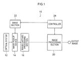
- Fig. 1 is a schematic block diagram illustrating an imaging apparatus 10 according to the present exemplary embodiment.
- the imaging apparatus 10 is configured including an optical system 12, an image pickup device 14, an image capture processing section 16, an image processing section 20, a drive section 22, and a controller 24.
- the optical system 12 is configured including for example a lens set configured from plural optical lenses, an aperture adjustment mechanism, a zoom mechanism, and an automatic focusing mechanism.
- the image pickup device 14 is what is referred to as a 1-chip image pickup device configured by an image pickup device, such as for example a Charge Coupled Device (CCD) or a Complementary Metal Oxide Semiconductor (CMOS) containing plural photoelectric conversion elements arrayed in the horizontal direction and vertical direction, with a color filter disposed above the image pickup device.
- an image pickup device such as for example a Charge Coupled Device (CCD) or a Complementary Metal Oxide Semiconductor (CMOS) containing plural photoelectric conversion elements arrayed in the horizontal direction and vertical direction, with a color filter disposed above the image pickup device.
- CCD Charge Coupled Device
- CMOS Complementary Metal Oxide Semiconductor
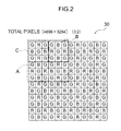
- Fig. 2 illustrates a portion of a color filter 30 according to the present invention. Note that (4896 ⁇ 3264) pixels are provided as an example of the number of pixels with an aspect ratio of 3:2, however there is no limitation to such a number of pixels and aspect ratio. As illustrated in Fig.
- the color filter 30 is a color filter having a repeatedly disposed 6 ⁇ 6 pixel basic array pattern C configured with a first array pattern A and a second array pattern B disposed symmetrically about a point, wherein the first array pattern A has a first filter G (referred to below as G filter) corresponding to G (green) that contributes most to obtaining a brightness signal placed at the 4 corner and center pixels of a 3 ⁇ 3 pixel square array, a second filter R (referred to below as R filter) corresponding to R (red) placed in the line at the horizontal direction center of the square array, and a third filter B (referred to below as B filter) corresponding to B (blue) placed in the line at the vertical direction center of the square array, and the second array pattern B has the same placement of the G filter as that of the first basic array pattern A and has the placement of the R filter and the placement of the B filter swapped over thereto.
- G filter first filter G
- R filter corresponding to R (red) placed in the line at the horizontal direction center of the square array
- the color filter 30 has the following features (1), (2), (3), (4) and (5).
- the color filter 30 illustrated in Fig. 2 includes the basic array pattern C formed from square placement patterns corresponding to 6 ⁇ 6 pixels, with the basic array pattern C disposed so as to repeat in both the horizontal direction and the vertical direction.
- the color filter array is an array in which each of the filters R, G, B (the R filter, G filter, B filter) has a specific periodicity.
- the color filter array of the thinning processed reduced image can be made similar to the color filter array prior to thinning processing, enabling a common processing circuit to be employed.
- the color filter 30 illustrated in Fig. 2 has the G filter, that corresponds to the color contributing the most to obtaining a brightness signal (the color G in the present exemplary embodiment), placed in each line in the horizontal direction, vertical direction and diagonal directions of the color filter array.
- the G filter corresponding to the brightness system pixels are placed in every line in the horizontal direction, vertical direction and diagonal directions of the color filter array, thereby enabling the reproduction precision of synchronization processing to be raised in the high frequency region, irrespective of the high frequency direction.
- the R filter and B filter that correspond to the two or more other colors than the G color (the R and B colors in the present exemplary embodiment), are placed in each line in the horizontal direction and vertical direction of the color filter array.
- the R filter and B filter are placed in each line in the horizontal direction and vertical direction of the color filter array, thereby enabling color moire (false color) generation to be suppressed.
- an optical low pass filter for suppressing false color generation may be omitted from placement on the optical path of the optical system from the incident face to the imaging plane.
- the basic array pattern C such as illustrated in Fig. 2 can be considered as an array of alternate first array pattern A and second array pattern B in the horizontal direction and vertical direction, wherein the first array pattern A is the 3 ⁇ 3 pixels surrounded by the frame of the broken line, and the second array pattern B is the 3 ⁇ 3 pixels surrounded by the frame of the single dot intermittent line.
- the first array pattern A and the second array pattern B both have the G filters for the respective brightness system pixels placed at their 4 corners and center, so as to be placed along their two diagonals. Moreover, in the first array pattern A, the B filters are arrayed in the horizontal direction on each side of the central G filter, and the R filters are arrayed in the vertical direction. However, in the second array pattern B, the R filters are arrayed on each side of the central G filter in the horizontal direction, and the B filters are arrayed in the vertical direction. Namely, the first array pattern A and the second array pattern B have reverse positional relationships for the R filters and the B filters, but have the same placement otherwise.
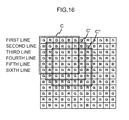
- the G filters at the 4 corners of the first array pattern A and the second array pattern B configure G filters that are arrayed in a square array corresponding to 2 ⁇ 2 pixels by disposing the first array pattern A and the second array pattern B alternately along the horizontal and vertical directions as illustrated in Fig. 16 .
- the color filter 30 illustrated in Fig. 2 contains a square array corresponding to 2 ⁇ 2 pixels formed from the G filters.
- the data of the G pixels with the smallest inter pixel separations are employed, thereby enabling determination of the direction with the highest correlation out of the horizontal direction, vertical direction and diagonal directions.
- the result of this directional determination can then be employed in interpolation processing from the peripheral pixels (synchronization processing).
- the basic array pattern C of the color filter 30 illustrated in Fig. 2 has point symmetry about the center of the basic array pattern C (the center of the 4 G filters). Moreover, as illustrated in Fig. 2 , the first array pattern A and the second array pattern B inside the basic array pattern C also each have respective point symmetry about the G filters at their respective centers.
- the color filter arrays of the first and third lines out of the first to sixth horizontal direction lines are GRGGBG
- the color filter array of the second line is BGBRGR
- the color filter arrays of the fourth and sixth lines are GBGGRG
- the color filter array of the fifth line is RGRBGB.
- the basic array pattern C that is the basic array pattern with point symmetry is, for convenience, referred to as the basic array pattern.
- the image pickup device 14 has phase difference detection pixels placed in a predetermined pattern.
- Light-blocking portions 40 containing light-blocking films 40A that block light to the horizontal direction left half of a pixel, and light-blocking films 40B that block light to the horizontal direction right half of a pixel are formed on the phase difference detection pixels as illustrated in Fig. 3 .
- phase difference AF control a phase shift amount is detected based on pixel data from the phase difference detection pixels provided with the light-blocking films 40A and based on pixel data from the phase difference detection pixels provided with the light-blocking films 40B.
- the focal position of the imaging lens is then adjusted based thereon.
- the light-blocking portions 40 are respectively provided on the phase difference detection pixels at the centers of 2 pairs of a first array pattern A and a second array pattern B, and are placed in all of the basic array patterns C.
- a light-blocking film 40A is provided to the phase difference detection pixel at (2, 2) and a light-blocking film 40B is provided to the phase difference detection pixel at (5, 5).
- a light-blocking film 40A is provided to the phase difference detection pixel at (5, 2) and a light-blocking film 40B is provided to the phase difference detection pixel at (2, 5).
- the light-blocking films 40A and the light-blocking films 40B are respectively formed on each of the phase difference detection pixels at the centers of the two pairs of first array pattern A and second array pattern B, as pairs of the first array pattern A and second array pattern B respectively disposed on the diagonals of the basic array pattern C.
- Such basic array patterns C are then disposed in rows in the horizontal direction and the vertical direction. Note that in Fig.
- the light-blocking portions 40 are provided in all of the basic array patterns C, however there is no limitation thereto, and they may be provided only in the basic array patterns C within a specific region of a section of the image pickup device. This also applies to other exemplary embodiments below.
- the light-blocking films 40A or the light-blocking films 40B are accordingly placed on the center pixels where the G filters are placed in the first array pattern A and the second array pattern B, with these pixels serving as the phase difference detection pixels.
- 4 individual G filters are placed at the periphery of these phase difference detection pixels.
- the pixel data of the phase difference detection pixels needs to be interpolated from the peripheral pixels, however there are the 4 individual G filters placed at the periphery thereof.
- the interpolation precision can accordingly be raised in cases in which for example video image capture and still image capture is carried out while performing phase difference AF control.
- the image capture processing section 16 subjects the image capture signals that have been output from the image pickup device 14 to predetermined processing, such as amplification processing and correlated double sampling, and A/D conversion processing, then outputs these as pixel data to the image processing section 20.
- predetermined processing such as amplification processing and correlated double sampling, and A/D conversion processing
- the image processing section 20 subjects the pixel data that has been output from the image capture processing section 16 to what is referred to as synchronization processing. Namely, for all the pixels, interpolation is performed of pixel data for colors other than the corresponding respective color from pixel data of peripheral pixels, so as to generate R, G, B pixel data for all pixels. Then, what is referred to as YC conversion processing is performed to the generated R, G, B pixel data, to generate brightness data Y and color difference data Cr, Cb. Then resizing processing is performed to re-size these signals to a size according to the image capture mode.
- the drive section 22 performs for example driving to read image capture signals from the image pickup device 14 according to instruction from the controller 24.
- the controller 24 performs overall control of the drive section 22 and the image processing section 20 according to the image capture mode. Although discussed in detail later, put briefly the controller 24 instructs the drive section 22 to read image capture signals with a reading method corresponding to the image capture mode, and instructs the image processing section 20 to perform image processing corresponding to the image capture mode.
- the controller 24 instructs the drive section 22 so as to thin and read image capture signals using a thinning method corresponding to the instructed image capture mode.
- image capture modes include a still image mode that captures still images, and video modes such as an HD video mode that thins the captured image and generates High Definition (HD) video data at a comparatively high definition and records this on a recording medium such as a memory card, not illustrated in the drawings, and a through video mode (live view mode) in which a captured image is thinned and a through video of comparatively low definition is output to a display section, not illustrated in the drawings.
- HD High Definition
- the drive section 22 is instructed to read pixel data by a thinning method corresponding to the image capture mode.
- Phase difference AF control is performed based on the pixel data of these lines, and other lines, namely at least some of the normal pixel lines, are also read and video data generated.
- interpolation is performed for the phase difference detection pixels from the pixel data of the normal pixels in their periphery.
- the phase difference detection pixels are placed on the pixels disposed with the G filters at the center of the first array patterns A and the second array patterns B, with 4 individual G filters placed at their periphery.
- the interpolation precision can accordingly be raised when pixel data for the phase difference detection pixels is interpolated from the peripheral pixels in cases in which for example video image capture and still image capture is carried out while performing phase difference AF control.
- the filter disposed on the phase difference detection pixels is the filter corresponding to G to which the human eye is particularly sensitive, thereby enabling the precision of phase difference AF control to be raised.
- the image processing section 20 is instructed to execute image processing (synchronization processing and YC conversion processing) and resizing processing corresponding to the image capture mode.
- the image pickup device 14 is a single-chip color image pickup device and so the output image thereof is a RAW image (mosaic image), with the need to obtain a multi-channel image by interpolation processing (synchronization processing) of missing color pixels from pixels at their periphery.
- the issue here is in the regeneration characteristics of high frequency image signals.
- the color filter 30 has the 2 ⁇ 2 G filters placed at the center of the basic array pattern C, and these pixels are normal pixels rather than phase difference detection pixels.
- the brightness correlation direction is determined based on pixel data of G pixels that are normal pixels where the 2 ⁇ 2 G filter described above is placed, and the pixel values of the other color pixels can be estimated with good precision by employing the pixel values of the other color pixels present in the direction determined to be the correlation direction, thereby suppressing false color from occurring in high frequency portions.
- G pixels of 2 ⁇ 2 pixels corresponding to G filters are extracted from a mosaic image output from the image pickup device 14, and when the pixel values of each of the G pixels are denoted G1, G2, G3, G4, in sequence from the top left to the bottom right, a direction determination circuit contained in the synchronization processing circuit computes the difference absolute values separately for each of the directions.
- the vertical direction difference absolute value is (
- the horizontal direction difference absolute value is (
- the bottom left-top right diagonal direction difference absolute value is (
- the top left-bottom right diagonal direction difference absolute value is (
- the direction determination circuit determines correlation (the correlation direction) as the direction having the smallest difference absolute value from out of these four correlation absolute values.
- a 5 ⁇ 5 pixel local region is extracted from the mosaic image such that the 3 ⁇ 3 pixel array A (see Fig. 2 ) is positioned at its center, there are 2 ⁇ 2 pixels of G pixels placed at the 4 corners of the 5 ⁇ 5 pixel local region. Consequently, when the 3 ⁇ 3 pixels of the array A inside the above local region are pixels subject to synchronization processing, the sums (or the average values) of the correlation absolute values of the 4 corners are derived separately for each direction, and the direction having the smallest value out of the sums (or the average values) of the correlation absolute values of the 4 corners for each of the directions is determined as the brightness correlation direction of the pixels subject to synchronization processing.
- the vertical direction difference absolute value sum of the pixel values of the 4 corner 2 ⁇ 2 G pixels illustrated in Fig. 7B is
- ⁇ 8 2040
- the horizontal direction difference absolute value sum is also
- ⁇ 8 2040.
- the bottom left-top right diagonal direction difference absolute value sum is
- ⁇ 2 0, and the top left-bottom right diagonal direction difference absolute value sum is
- ⁇ 2 0.
- the directions with the smallest difference absolute value sums are the 2 directions of the bottom left-top right diagonal direction and the top left-bottom right diagonal direction.
- the directions with the smallest difference absolute value sums are the 2 directions of the bottom left-top right diagonal direction and the top left-bottom right diagonal direction.
- either of the diagonal directions may be employed without a problem arising.
- the correlation direction is determined from the mutually adjacent 2 ⁇ 2 pixels of G pixels as described above, the correlation direction can be determined using the minimum pixel separation. Namely, the correlation direction can be determined with good precision without being influenced by high frequencies.
- the synchronization processing circuit When the correlation direction of the pixels subject to synchronization processing has been determined, the synchronization processing circuit then employs the pixel values of the other color pixels present in the determined correlation direction during computation of the other color pixel values of the pixel positions of the pixels subject to synchronization processing.
- the R pixel value at the pixel position of the G22 pixel is taken to be the unadjusted R12 or R32 pixel value, or determined by interpolation from the R12 and R32 pixel values.
- the B pixel value at the pixel position of the G22 pixel is taken to be the unadjusted B02 or B42 pixel value, or determined by interpolation from the B02 and B42 pixel values.
- the R pixel value at the pixel position of the B02 pixel is taken to be the unadjusted R12 pixel value, or determined by interpolation from the R12 and R32 pixel values.
- the G pixel value at the pixel position of the B02 pixel is taken to be the unadjusted G22 pixel value, or determined by interpolation from the pixel value of the G pixel in the same horizontal position in the adjacent array B and the pixel value of the G22.
- the other color pixel values are computed by interpolating pixel values of subject pixels by computing color differences of pixel values of the R, B pixels in the vicinity of the G pixels.
- the pixel values G12', G21' are G pixel values at pixel positions of the R12, B21 pixels estimated by top left-bottom right diagonal direction determination.
- the pixel values R22', B22' of the R, B pixels at the pixel position of the G22 pixel employ color differences between each of the pixel positions of the B21, B23 pixels and the R12, R32 pixels in the vicinity thereof to interpolate the pixel value G22 of G22, and compute the R, G pixel values R22', B22' at the pixel position of the G22 pixel.
- R ⁇ 22 ⁇ ⁇ G ⁇ 22 + R ⁇ 12 + R ⁇ 32 / 2 - G ⁇ 12 ⁇ ⁇ + G ⁇ 32 ⁇ ⁇ / 2
- B ⁇ 22 ⁇ ⁇ G ⁇ 22 + B ⁇ 21 + B ⁇ 23 / 2 - G ⁇ 21 ⁇ ⁇ + G ⁇ 23 ⁇ ⁇ / 2
- the other color pixel values can be computed by interpolating the pixel values of subject pixels using color differences of the pixel values of pixels in the vicinity for which RGB pixel values have been computed.
- the method for computing other color pixel values by interpolating the pixel values of subject pixels using color difference of pixels in the vicinity is as set out below.
- a pixel subject to synchronization processing is a G pixel and its pixel value is denoted G and there are no R or B pixels present in the correlation direction determined by the direction determination circuit
- the pixel values of the R, B pixels in the vicinity of the G pixel are denoted R, B
- the G pixel values at the pixel positions of these pixels are denoted GR, GB
- the R, B pixel values RG, BG at the position of the subject pixel are computed according to the following equations.
- Equations (1) correspond to the equations (a) and (b) described above.
- the pixel subject to synchronization processing is an R pixel and its pixel value is denoted R and there are no G or B pixels present in the correlation direction determined by the direction determination circuit
- the pixel values of the G, B pixels in the vicinity of the R pixel are denoted G, B
- the R pixel values at the pixel positions of these pixels are denoted RG, RB
- the G, B pixel values GR, BR at the position of the subject pixel are computed according to the following equations.
- GR R + G - RG
- BR R + B - RB
- the pixel subject to synchronization processing is a B pixel and its pixel value is denoted B and there are no G or R pixels present in the correlation direction determined by the direction determination circuit
- the pixel values of the G, R pixels in the vicinity of the B pixel are denoted G. R
- the B pixel values at the pixel positions of these pixels are denoted BG, BR
- the G, R pixel values GB, RB at the position of the subject pixel are computed according to the following equations.
- GB B + G - BG
- RB B + R - BR
- the other color pixel values are computed by interpolation of the pixel values of the subject pixels using the color difference of other color pixels in the vicinity
- Configuration may be made such that the other color pixel values are computed by interpolating the pixel values of the subject pixels by a color ratio of other color pixels in the vicinity.
- a specific example is given below of a method for interpolating pixel values for a subject pixel to so at to compute the other color pixel values using a color ratio of pixels in the vicinity.
- a pixel subject to synchronization processing is a G pixel and its pixel value is denoted G and there are no R or B pixels present in the correlation direction determined by the direction determination circuit
- the pixel values of the R, B pixels in the vicinity of the G pixel are denoted R, B
- the G pixel values at the pixel positions of these pixels are denoted GR, GB
- the R, B pixel values RG, BG at the position of the subject pixel are computed according to the following equations.
- the pixel subject to synchronization processing is an R pixel and its pixel value is denoted R and there are no G or B pixels present in the correlation direction determined by the direction determination circuit
- the pixel values of the G, B pixels in the vicinity of the R pixel are denoted G, B
- the R pixel values at the pixel positions of these pixels are denoted RG, RB
- the G, B pixel values GR, BR at the position of the subject pixel are computed according to the following equations.
- GR R ⁇ G / RG
- BR R ⁇ B / RB
- the pixel subject to synchronization processing is a B pixel and its pixel value is denoted B and there are no G or R pixels present in the correlation direction determined by the direction determination circuit
- the pixel values of the G, R pixels in the vicinity of the B pixel are denoted G, R
- the B pixel values at the pixel positions of these pixels are denoted BG, BR
- the G, R pixel values GB, RB at the position of the subject pixel are computed according to the following equations.
- GB B ⁇ G / BG
- RB B ⁇ R / BR
- the direction determination circuit determines that there is no correlation direction.
- the other color pixel values at the pixel positions of the pixels subject to synchronization processing employ the pixel values of the other color pixels present in the vicinity of these pixel positions.
- controller 24 may be configured with a computer that includes a CPU, ROM, RAM and non-volatile ROM.
- a processing program for the above processing may, for example, be pre-stored on the non-volatile ROM, and then executed by reading into the CPU.
- Fig. 9 illustrates a placement of light-blocking films 40A, 40B according to the present exemplary embodiment.
- a point of difference of the present exemplary embodiment to the first exemplary embodiment is the placement of the light-blocking films 40A, 40B.
- the light-blocking portions 40 are respectively provided on the phase difference detection pixels at the center of 2 pairs a first array pattern A and a second array pattern B that configure a basic array pattern C, with horizontal direction array lines of the first array pattern A and the second array pattern B that are placed with the light-blocking portions 40 alternating in the vertical direction with horizontal direction array lines of the first array pattern A and the second array pattern B that are not placed with the light-blocking portions 40.
- a first array pattern A and a second array pattern B that configure a basic array pattern C, with horizontal direction array lines of the first array pattern A and the second array pattern B that are placed with the light-blocking portions 40 alternating in the vertical direction with horizontal direction array lines of the first array pattern A and the second array pattern B that are not placed with the light-blocking portions 40.
- the light-blocking films 40A, 40B are placed in the vertical direction (2n + 1) th lines of the basic array patterns C, and the light-blocking films 40A, 40B are not placed in the (2n + 2) th lines of the basic array patterns C.
- the controller 24 reads pixel data of the phase difference detection pixels placed with the light-blocking films 40A, 40B in the vertical direction (2n + 1) th lines of the basic array patterns C and performs phase difference AF control, and also reads pixel data of normal pixels in the vertical direction (2n + 2) th lines of the basic array patterns C and generates video data.
- the pixel data from the phase difference detection pixels is only employed for phase difference AF control, and is not used in generating video data and so there is no need for interpolation from the peripheral pixels.
- the video data is generated from pixel data of normal pixels.
- the processing speed for phase difference AF control can be raised in comparison to cases in which the phase difference detection pixels are generated based on video data.
- the processing speed for video data generation can be raised in comparison to cases in which interpolated video data is generated.
- Fig. 10 illustrates a placement of light-blocking films 40A, 40B according to the present exemplary embodiment.
- a point of difference of the present exemplary embodiment to the first exemplary embodiment is the placement of the light-blocking films 40A, 40B.
- Thinning driving is similar to that of the second exemplary embodiment.
- the light-blocking portions 40 are provided on the phase difference detection pixels at the center of a first array pattern C and a second array pattern B on one horizontal direction side out of two pairs of the array pattern A and the second array pattern B that configure a basic array pattern C, with horizontal direction array lines of the first array patterns A and the second array patterns B that are placed with the light-blocking portions 40 disposed alternately in the vertical direction with horizontal direction array lines of the first array patterns A and the second array patterns B that are not placed with the light-blocking portions 40.
- the precision of interpolation can be raised, enabling image quality to be raised.
- Fig. 11 illustrates a placement of light-blocking films 40A, 40B according to the present exemplary embodiment.
- a point of difference of the present exemplary embodiment to the above exemplary embodiment is the placement of the light-blocking films 40A, 40B.
- Thinning driving is similar to that of the first exemplary embodiment.
- the light-blocking portions 40 are provided on the phase difference detection pixels at the centers of 2 first array patterns A disposed on one diagonal of a basic array pattern C, and are placed in all the basic array patterns.
- the horizontal direction adjacent pixel on the side provided with the light-blocking film 40A of the phase difference detection pixels where the light-blocking films 40A are provided and the horizontal direction adjacent pixel on the side provided with the light-blocking film 40B of the phase difference detection pixels where the light-blocking films 40B are provided are both the same as each other, namely B pixels.
- the influence from color mixing can accordingly be cancelled out, and the image quality can be raised compared to cases in which the horizontal direction adjacent pixel on the side provided with the light-blocking film 40A of the phase difference detection pixels where the light-blocking films 40A are provided and the horizontal direction adjacent pixel on the side provided with the light-blocking film 40B of the phase difference detection pixels where the light-blocking films 40B are provided are not the same as each other.
- configuration may be made with provision on the phase difference detection pixels at the center of the 2 second array patterns B disposed on the other diagonal of the basic array pattern C, and are placed in all the basic array patterns.
- the horizontal direction adjacent pixel on the side provided with the light-blocking film 40A of the phase difference detection pixels where the light-blocking films 40A are provided and the horizontal direction adjacent pixel on the side provided with the light-blocking film 40B of the phase difference detection pixels where the light-blocking films 40B are provided are both the same as each other, namely R pixels. Since the wavelength of R is particularly susceptible to being incident to the adjacent pixels, color mixing can be even more efficiently prevented, enabling the image quality to be raised.
- Fig. 13 illustrates a placement of the light-blocking films 40A, 40B according to the present exemplary embodiment.
- a point of difference of the present exemplary embodiment to the above exemplary embodiment is the placement of the light-blocking films 40A, 40B.
- the thinning driving is similar to that of the second and third exemplary embodiments.
- the light-blocking portions 40 are respectively provided on the phase difference detection pixels at the centers of 2 first array patterns B that are disposed on one of the diagonals of a basic array pattern C, with horizontal direction array lines of the basic array patterns C that are placed with the light-blocking portions 40 arrayed alternating in the vertical direction with horizontal direction array lines of the basic array patterns C that are not placed with the light-blocking portions 40.
- the horizontal direction adjacent pixel on the side provided with the light-blocking film 40A of the phase difference detection pixels where the light-blocking films 40A are provided and the horizontal direction adjacent pixel on the side provided with the light-blocking film 40B of the phase difference detection pixels where the light-blocking films 40B are provided are both the same as each other, namely B pixels.
- the influence from color mixing can accordingly be cancelled out, and the image quality can be raised compared to cases in which the horizontal direction adjacent pixel on the side provided with the light-blocking film 40A of the phase difference detection pixels where the light-blocking films 40A are provided and the horizontal direction adjacent pixel on the side provided with the light-blocking film 40B of the phase difference detection pixels where the light-blocking films 40B are not the same as each other.
- the controller 24 reads pixel data of the phase difference detection pixels placed with the light-blocking films 40A, 40B in the vertical direction (2n + 1) th lines of the basic array patterns C to perform phase difference AF control, and also reads pixel data of normal pixels in the vertical direction (2n + 2) th lines of the basic array patterns C to generate video data.
- the pixel data from the phase difference detection pixels is only employed for phase difference AF control, and is not used in generating video data and so the there is no need for interpolation from the peripheral pixels.
- the video data is generated from pixel data of normal pixels.
- the processing speed for phase difference AF control can be raised in comparison to cases in which the phase difference detection pixels are based on video data generation.
- the processing speed for video data generation can be raised in comparison to cases in which video data is generated by interpolation.
- configuration may be made such respective provision is made on the phase difference detection pixels at the centers of 2 second array patterns B that are disposed on the other of the diagonals, with horizontal direction array lines of the basic array patterns C that are placed with the light-blocking portions 40 arrayed alternating in the vertical direction with horizontal direction array lines of the basic array patterns C that are not placed with the light-blocking portions 40.
- the horizontal direction adjacent pixel on the side provided with the light-blocking film 40A of the phase difference detection pixels where the light-blocking films 40A are provided and the horizontal direction adjacent pixel on the side provided with the light-blocking film 40B of the phase difference detection pixels where the light-blocking films 40B are provided are both the same as each other, namely R pixels. Since the wavelength of R is particularly susceptible to being incident to the adjacent pixels, color mixing can be even more efficiently prevented, enabling the image quality to be raised.
- phase difference detection pixels may be formed by adopting the configuration described in Japanese Patent Application 2009-227338 .
- an image pickup device configured by top microlenses, inner microlenses, and the light receiving elements of similar shape, configured to include first pixels D1 that receive light rays that have passed through the entire region of the imaging lens eye, second pixels D2 that receive only light rays that passed through a portion of a half region of the imaging lens eye, and third pixels D3 that receive only light rays that have passed through a portion of a half region of the imaging lens eye that is different to the second pixels D2.
- top microlenses L2, L3 are disposed on the second pixels D2 and the third pixels D3, the top microlenses L2, L3 having a smaller diameter than top microlenses L1 for the first pixels D1 and being respectively shifted in different directions with respect to the optical axes of the inner microlenses.
- the top microlenses and the light receiving elements are disposed shifted with respect to each other.
- the second pixels D2 and the third D3 can accordingly be formed in this manner as the phase difference detection pixels.
- the present invention is also applicable to such a configuration.
- an embodiment may also be implemented without provision of the inner lenses.
- the configuration of the phase difference pixels is not limited to the configuration described above, and it is possible to substitute any configuration capable of partitioning the eye.
- phase difference detection pixels have a lower sensitivity than normal pixels, and their characteristics are also differ, there is a need to correct the pixel data from phase difference detection pixels when the pixel data of the phase difference detection pixels is employed as imaging data for a still image or a video image.
- a pixel data correction method for phase difference detection pixels in the present exemplary embodiment.
- Average value correction is a method in which an average value of the pixel values of normal pixels at the periphery of the phase difference detection pixels is taken as pixel data for these phase difference detection pixels.
- Gain correction is a method by which pixel data for the phase difference detection pixels is raised by multiplying pixel data for the phase difference detection pixels by a specific gain equivalent to the difference in level between the normal pixels and the phase difference detection pixels.
- Fig. 17 illustrates a placement of G pixels in 3 ⁇ 3 pixels that are centered on a G pixel at the center of an array A and an array B.
- the G pixel at the center is G1
- the G pixels at the periphery thereof are respectively G2, G3, G4, G5, clockwise from the top left.
- the phase difference detection pixels are each placed at the G1 pixel of Fig. 17 .
- the average value of the pixel data of each of the G2, G3, G4 and G5 pixels that are normal pixels at the periphery thereof is taken as the pixel data for the G1 pixel.
- Average value correction for the pixel data of phase difference detection pixels is accordingly performed as above based on the pixel data of the peripheral normal pixels.
- gain correction or average value correction may be chosen according to the contents of the captured image.
Landscapes
- Engineering & Computer Science (AREA)
- Multimedia (AREA)
- Signal Processing (AREA)
- Physics & Mathematics (AREA)
- Spectroscopy & Molecular Physics (AREA)
- General Physics & Mathematics (AREA)
- Color Television Image Signal Generators (AREA)
- Focusing (AREA)
- Automatic Focus Adjustment (AREA)
- Transforming Light Signals Into Electric Signals (AREA)
Applications Claiming Priority (3)
| Application Number | Priority Date | Filing Date | Title |
|---|---|---|---|
| JP2011066629 | 2011-03-24 | ||
| JP2011163308 | 2011-07-26 | ||
| PCT/JP2011/067546 WO2012127699A1 (ja) | 2011-03-24 | 2011-07-29 | カラー撮像素子、撮像装置、及び撮像プログラム |
Publications (2)
| Publication Number | Publication Date |
|---|---|
| EP2690873A1 true EP2690873A1 (de) | 2014-01-29 |
| EP2690873A4 EP2690873A4 (de) | 2014-10-08 |
Family
ID=46878890
Family Applications (1)
| Application Number | Title | Priority Date | Filing Date |
|---|---|---|---|
| EP11861733.1A Withdrawn EP2690873A4 (de) | 2011-03-24 | 2011-07-29 | Bildgebungselement, bildgebungsvorrichtung und bildgebungsprogramm |
Country Status (5)
| Country | Link |
|---|---|
| US (1) | US8723991B2 (de) |
| EP (1) | EP2690873A4 (de) |
| JP (1) | JP5547338B2 (de) |
| CN (1) | CN103444183B (de) |
| WO (1) | WO2012127699A1 (de) |
Families Citing this family (12)
| Publication number | Priority date | Publication date | Assignee | Title |
|---|---|---|---|---|
| WO2012127701A1 (ja) * | 2011-03-24 | 2012-09-27 | 富士フイルム株式会社 | カラー撮像素子、撮像装置、及び撮像プログラム |
| WO2014007279A1 (ja) * | 2012-07-06 | 2014-01-09 | 富士フイルム株式会社 | カラー撮像素子および撮像装置 |
| JP5777825B2 (ja) * | 2012-12-05 | 2015-09-09 | 富士フイルム株式会社 | 撮像装置、異常斜め入射光検出方法及びプログラム、並びに記録媒体 |
| CN104838646B (zh) * | 2012-12-07 | 2016-11-23 | 富士胶片株式会社 | 图像处理装置、图像处理方法、程序及记录介质 |
| JP6630058B2 (ja) * | 2014-06-16 | 2020-01-15 | キヤノン株式会社 | 撮像装置、撮像装置の制御方法、及び、プログラム |
| JP6364259B2 (ja) * | 2014-07-02 | 2018-07-25 | オリンパス株式会社 | 撮像装置、画像処理方法、及び画像処理プログラム |
| KR102346622B1 (ko) * | 2014-08-04 | 2022-01-04 | 엘지이노텍 주식회사 | 이미지 센서 및 이를 포함하는 촬상 장치 |
| KR102269600B1 (ko) * | 2014-08-05 | 2021-06-25 | 삼성전자주식회사 | 위상차 포커스 검출 가능한 촬상소자 |
| JP2018046394A (ja) * | 2016-09-14 | 2018-03-22 | オリンパス株式会社 | 撮像素子、撮像装置 |
| US10366674B1 (en) | 2016-12-27 | 2019-07-30 | Facebook Technologies, Llc | Display calibration in electronic displays |
| US11245878B2 (en) * | 2019-02-28 | 2022-02-08 | Qualcomm Incorporated | Quad color filter array image sensor with aperture simulation and phase detection |
| KR102926334B1 (ko) * | 2021-07-01 | 2026-02-13 | 삼성전자주식회사 | 이미지 센서 |
Family Cites Families (26)
| Publication number | Priority date | Publication date | Assignee | Title |
|---|---|---|---|---|
| JPH0823543A (ja) | 1994-07-07 | 1996-01-23 | Canon Inc | 撮像装置 |
| JPH0823542A (ja) | 1994-07-11 | 1996-01-23 | Canon Inc | 撮像装置 |
| JP3935548B2 (ja) | 1997-02-27 | 2007-06-27 | オリンパス株式会社 | 画像信号処理装置 |
| EP0930789B1 (de) | 1998-01-20 | 2005-03-23 | Hewlett-Packard Company, A Delaware Corporation | Farbbildaufnahmegerät |
| JP3592147B2 (ja) | 1998-08-20 | 2004-11-24 | キヤノン株式会社 | 固体撮像装置 |
| JP4098438B2 (ja) | 1999-04-15 | 2008-06-11 | オリンパス株式会社 | カラー撮像素子及びカラー撮像装置 |
| US6707937B1 (en) * | 2000-07-14 | 2004-03-16 | Agilent Technologies, Inc. | Interpolation of edge portions of a digital image |
| JP4088959B2 (ja) * | 2001-01-09 | 2008-05-21 | ソニー株式会社 | 画像処理装置および方法、並びに記録媒体 |
| JP4019417B2 (ja) | 2003-01-14 | 2007-12-12 | ソニー株式会社 | 画像処理装置および方法、記録媒体、並びにプログラム |
| JP2004266369A (ja) | 2003-02-21 | 2004-09-24 | Sony Corp | 固体撮像装置およびその駆動方法 |
| JP4385282B2 (ja) | 2003-10-31 | 2009-12-16 | ソニー株式会社 | 画像処理装置および画像処理方法 |
| JP4797606B2 (ja) | 2005-12-01 | 2011-10-19 | 株式会社ニコン | 撮像装置 |
| US7821553B2 (en) | 2005-12-30 | 2010-10-26 | International Business Machines Corporation | Pixel array, imaging sensor including the pixel array and digital camera including the imaging sensor |
| JP4662883B2 (ja) | 2006-05-15 | 2011-03-30 | 富士フイルム株式会社 | 二次元カラー固体撮像素子 |
| US7769230B2 (en) * | 2006-11-30 | 2010-08-03 | Eastman Kodak Company | Producing low resolution images |
| US7701496B2 (en) * | 2006-12-22 | 2010-04-20 | Xerox Corporation | Color filter pattern for color filter arrays including a demosaicking algorithm |
| JP5082528B2 (ja) | 2007-03-23 | 2012-11-28 | ソニー株式会社 | 固体撮像装置及び撮像装置 |
| JP5040458B2 (ja) | 2007-06-16 | 2012-10-03 | 株式会社ニコン | 固体撮像素子及びこれを用いた撮像装置 |
| WO2009020031A1 (en) * | 2007-08-06 | 2009-02-12 | Canon Kabushiki Kaisha | Image sensing apparatus |
| JP5029268B2 (ja) * | 2007-10-01 | 2012-09-19 | 株式会社ニコン | 電子カメラ |
| JP5092685B2 (ja) | 2007-10-23 | 2012-12-05 | 株式会社ニコン | 撮像素子および撮像装置 |
| JP5063627B2 (ja) | 2008-02-28 | 2012-10-31 | 中国電力株式会社 | 作業服類の保管袋及びこれを用いた保管方法 |
| EP3328048B1 (de) | 2008-05-20 | 2021-04-21 | FotoNation Limited | Aufnahme und verarbeitung von bildern mittels monolithischer kamera anordnung mit heterogenem bildwandler |
| JP2010066494A (ja) | 2008-09-10 | 2010-03-25 | Olympus Corp | 固体撮像素子及びデジタルカメラ |
| JP5149143B2 (ja) | 2008-12-24 | 2013-02-20 | シャープ株式会社 | 固体撮像素子およびその製造方法、電子情報機器 |
| JP5471117B2 (ja) * | 2009-07-24 | 2014-04-16 | ソニー株式会社 | 固体撮像装置とその製造方法並びにカメラ |
-
2011
- 2011-07-29 EP EP11861733.1A patent/EP2690873A4/de not_active Withdrawn
- 2011-07-29 JP JP2013505761A patent/JP5547338B2/ja not_active Expired - Fee Related
- 2011-07-29 CN CN201180069495.8A patent/CN103444183B/zh not_active Expired - Fee Related
- 2011-07-29 WO PCT/JP2011/067546 patent/WO2012127699A1/ja not_active Ceased
-
2013
- 2013-09-19 US US14/031,822 patent/US8723991B2/en not_active Expired - Fee Related
Also Published As
| Publication number | Publication date |
|---|---|
| CN103444183A (zh) | 2013-12-11 |
| EP2690873A4 (de) | 2014-10-08 |
| US8723991B2 (en) | 2014-05-13 |
| JPWO2012127699A1 (ja) | 2014-07-24 |
| US20140043508A1 (en) | 2014-02-13 |
| CN103444183B (zh) | 2015-01-28 |
| WO2012127699A1 (ja) | 2012-09-27 |
| JP5547338B2 (ja) | 2014-07-09 |
Similar Documents
| Publication | Publication Date | Title |
|---|---|---|
| EP2690873A1 (de) | Bildgebungselement, bildgebungsvorrichtung und bildgebungsprogramm | |
| US8730545B2 (en) | Color imaging element, imaging device, and storage medium storing a control program for imaging device | |
| JP5572765B2 (ja) | 固体撮像素子、撮像装置、及び合焦制御方法 | |
| US8736743B2 (en) | Color imaging element, imaging device, and storage medium storing a control program for imaging device | |
| US8723992B2 (en) | Color imaging element, imaging device, and storage medium storing an imaging program | |
| US8928785B2 (en) | Imaging device and storage medium storing an imaging program | |
| US8842214B2 (en) | Color imaging element, imaging device, and storage medium storing an imaging program | |
| US8723993B2 (en) | Imaging device and storage medium storing an imaging program | |
| US8804016B2 (en) | Color imaging element, imaging device, and storage medium storing an imaging program | |
| US9485482B2 (en) | Imaging device, method for controlling imaging device, and storage medium storing a control program for color mixing correction | |
| JP5607266B2 (ja) | 撮像装置、撮像装置の制御方法、及び制御プログラム | |
| JP5634614B2 (ja) | 撮像素子及び撮像装置 | |
| US8958000B2 (en) | Imaging device, method for controlling imaging device, and storage medium storing a control program | |
| US9113027B2 (en) | Imaging device, method for controlling imaging device, and storage medium storing a control program |
Legal Events
| Date | Code | Title | Description |
|---|---|---|---|
| PUAI | Public reference made under article 153(3) epc to a published international application that has entered the european phase |
Free format text: ORIGINAL CODE: 0009012 |
|
| 17P | Request for examination filed |
Effective date: 20130923 |
|
| AK | Designated contracting states |
Kind code of ref document: A1 Designated state(s): AL AT BE BG CH CY CZ DE DK EE ES FI FR GB GR HR HU IE IS IT LI LT LU LV MC MK MT NL NO PL PT RO RS SE SI SK SM TR |
|
| DAX | Request for extension of the european patent (deleted) | ||
| A4 | Supplementary search report drawn up and despatched |
Effective date: 20140910 |
|
| RIC1 | Information provided on ipc code assigned before grant |
Ipc: H04N 5/232 20060101ALI20140904BHEP Ipc: H04N 9/07 20060101AFI20140904BHEP |
|
| 17Q | First examination report despatched |
Effective date: 20151027 |
|
| STAA | Information on the status of an ep patent application or granted ep patent |
Free format text: STATUS: THE APPLICATION IS DEEMED TO BE WITHDRAWN |
|
| 18D | Application deemed to be withdrawn |
Effective date: 20161103 |