EP2693263A1 - Anzeigevorrichtung - Google Patents
Anzeigevorrichtung Download PDFInfo
- Publication number
- EP2693263A1 EP2693263A1 EP12190521.0A EP12190521A EP2693263A1 EP 2693263 A1 EP2693263 A1 EP 2693263A1 EP 12190521 A EP12190521 A EP 12190521A EP 2693263 A1 EP2693263 A1 EP 2693263A1
- Authority
- EP
- European Patent Office
- Prior art keywords
- cover member
- display device
- panel assembly
- display panel
- speaker
- Prior art date
- Legal status (The legal status is an assumption and is not a legal conclusion. Google has not performed a legal analysis and makes no representation as to the accuracy of the status listed.)
- Withdrawn
Links
Images


Classifications
-
- G—PHYSICS
- G02—OPTICS
- G02F—OPTICAL DEVICES OR ARRANGEMENTS FOR THE CONTROL OF LIGHT BY MODIFICATION OF THE OPTICAL PROPERTIES OF THE MEDIA OF THE ELEMENTS INVOLVED THEREIN; NON-LINEAR OPTICS; FREQUENCY-CHANGING OF LIGHT; OPTICAL LOGIC ELEMENTS; OPTICAL ANALOGUE/DIGITAL CONVERTERS
- G02F1/00—Devices or arrangements for the control of the intensity, colour, phase, polarisation or direction of light arriving from an independent light source, e.g. switching, gating or modulating; Non-linear optics
- G02F1/01—Devices or arrangements for the control of the intensity, colour, phase, polarisation or direction of light arriving from an independent light source, e.g. switching, gating or modulating; Non-linear optics for the control of the intensity, phase, polarisation or colour
- G02F1/13—Devices or arrangements for the control of the intensity, colour, phase, polarisation or direction of light arriving from an independent light source, e.g. switching, gating or modulating; Non-linear optics for the control of the intensity, phase, polarisation or colour based on liquid crystals, e.g. single liquid crystal display cells
- G02F1/133—Constructional arrangements; Operation of liquid crystal cells; Circuit arrangements
- G02F1/1333—Constructional arrangements; Manufacturing methods
- G02F1/133308—Support structures for LCD panels, e.g. frames or bezels
-
- H—ELECTRICITY
- H04—ELECTRIC COMMUNICATION TECHNIQUE
- H04N—PICTORIAL COMMUNICATION, e.g. TELEVISION
- H04N5/00—Details of television systems
- H04N5/64—Constructional details of receivers, e.g. cabinets or dust covers
-
- G—PHYSICS
- G02—OPTICS
- G02F—OPTICAL DEVICES OR ARRANGEMENTS FOR THE CONTROL OF LIGHT BY MODIFICATION OF THE OPTICAL PROPERTIES OF THE MEDIA OF THE ELEMENTS INVOLVED THEREIN; NON-LINEAR OPTICS; FREQUENCY-CHANGING OF LIGHT; OPTICAL LOGIC ELEMENTS; OPTICAL ANALOGUE/DIGITAL CONVERTERS
- G02F1/00—Devices or arrangements for the control of the intensity, colour, phase, polarisation or direction of light arriving from an independent light source, e.g. switching, gating or modulating; Non-linear optics
- G02F1/01—Devices or arrangements for the control of the intensity, colour, phase, polarisation or direction of light arriving from an independent light source, e.g. switching, gating or modulating; Non-linear optics for the control of the intensity, phase, polarisation or colour
- G02F1/13—Devices or arrangements for the control of the intensity, colour, phase, polarisation or direction of light arriving from an independent light source, e.g. switching, gating or modulating; Non-linear optics for the control of the intensity, phase, polarisation or colour based on liquid crystals, e.g. single liquid crystal display cells
- G02F1/133—Constructional arrangements; Operation of liquid crystal cells; Circuit arrangements
- G02F1/1333—Constructional arrangements; Manufacturing methods
- G02F1/133308—Support structures for LCD panels, e.g. frames or bezels
- G02F1/133311—Environmental protection, e.g. against dust or humidity
-
- G—PHYSICS
- G02—OPTICS
- G02F—OPTICAL DEVICES OR ARRANGEMENTS FOR THE CONTROL OF LIGHT BY MODIFICATION OF THE OPTICAL PROPERTIES OF THE MEDIA OF THE ELEMENTS INVOLVED THEREIN; NON-LINEAR OPTICS; FREQUENCY-CHANGING OF LIGHT; OPTICAL LOGIC ELEMENTS; OPTICAL ANALOGUE/DIGITAL CONVERTERS
- G02F1/00—Devices or arrangements for the control of the intensity, colour, phase, polarisation or direction of light arriving from an independent light source, e.g. switching, gating or modulating; Non-linear optics
- G02F1/01—Devices or arrangements for the control of the intensity, colour, phase, polarisation or direction of light arriving from an independent light source, e.g. switching, gating or modulating; Non-linear optics for the control of the intensity, phase, polarisation or colour
- G02F1/13—Devices or arrangements for the control of the intensity, colour, phase, polarisation or direction of light arriving from an independent light source, e.g. switching, gating or modulating; Non-linear optics for the control of the intensity, phase, polarisation or colour based on liquid crystals, e.g. single liquid crystal display cells
- G02F1/133—Constructional arrangements; Operation of liquid crystal cells; Circuit arrangements
- G02F1/1333—Constructional arrangements; Manufacturing methods
- G02F1/133308—Support structures for LCD panels, e.g. frames or bezels
- G02F1/133314—Back frames
-
- G—PHYSICS
- G02—OPTICS
- G02F—OPTICAL DEVICES OR ARRANGEMENTS FOR THE CONTROL OF LIGHT BY MODIFICATION OF THE OPTICAL PROPERTIES OF THE MEDIA OF THE ELEMENTS INVOLVED THEREIN; NON-LINEAR OPTICS; FREQUENCY-CHANGING OF LIGHT; OPTICAL LOGIC ELEMENTS; OPTICAL ANALOGUE/DIGITAL CONVERTERS
- G02F1/00—Devices or arrangements for the control of the intensity, colour, phase, polarisation or direction of light arriving from an independent light source, e.g. switching, gating or modulating; Non-linear optics
- G02F1/01—Devices or arrangements for the control of the intensity, colour, phase, polarisation or direction of light arriving from an independent light source, e.g. switching, gating or modulating; Non-linear optics for the control of the intensity, phase, polarisation or colour
- G02F1/13—Devices or arrangements for the control of the intensity, colour, phase, polarisation or direction of light arriving from an independent light source, e.g. switching, gating or modulating; Non-linear optics for the control of the intensity, phase, polarisation or colour based on liquid crystals, e.g. single liquid crystal display cells
- G02F1/133—Constructional arrangements; Operation of liquid crystal cells; Circuit arrangements
- G02F1/1333—Constructional arrangements; Manufacturing methods
- G02F1/133308—Support structures for LCD panels, e.g. frames or bezels
- G02F1/13332—Front frames
-
- G—PHYSICS
- G02—OPTICS
- G02F—OPTICAL DEVICES OR ARRANGEMENTS FOR THE CONTROL OF LIGHT BY MODIFICATION OF THE OPTICAL PROPERTIES OF THE MEDIA OF THE ELEMENTS INVOLVED THEREIN; NON-LINEAR OPTICS; FREQUENCY-CHANGING OF LIGHT; OPTICAL LOGIC ELEMENTS; OPTICAL ANALOGUE/DIGITAL CONVERTERS
- G02F2201/00—Constructional arrangements not provided for in groups G02F1/00 - G02F7/00
- G02F2201/50—Protective arrangements
- G02F2201/505—Arrangements improving the resistance to acoustic resonance like noise
Definitions
- the present invention relates to a display device such as a monitor or a television receiver that displays a video picture thereon.
- a thin display device with a liquid crystal cell having a small depth compared to the height and the width has been widely used.
- Such a thin display device is equipped with a circuit board which supplies power or a circuit board which controls a signal input from the outside and displays a video picture in the liquid crystal cell. Then, there have been various attempts to simplify a structure of the display device, realize a decrease in the weight and the thickness of the display device, or improve the designability of the display device.
- Japanese Patent Application Laid-Open No. 2000-315054 discloses a structure in which the inside of a casing formed by a front cabinet having a display window and a back cabinet disposed behind the front cabinet is provided with various circuit boards integrated with a display panel assembly having a member for displaying a video picture thereon and built in a space formed by a front bezel and a back chassis on the basis of a reinforcement plate. Accordingly, it is possible to decrease the number of steps of assembling the display device and to decrease the thickness of the display device.
- Japanese Patent Application Laid-Open No. 2007-163861 discloses a structure in which a display panel assembly, various substrates, and all inner components including a speaker are attached on the chassis as a reference and a front cabinet and a back cabinet are attached thereto. Accordingly, it is possible to simplify the assembly operation and the maintenance operation of the display device and to simplify the shapes of the front cabinet and the back cabinet.
- the assembly workability may be improved by attaching a part or the entirety of the inner components constituting the display device to the reinforcement plate or the chassis.
- the number of components consequently increases.
- the inner components are attached on the basis of the reinforcement plate or the chassis and the exterior of the device is formed by the front cabinet and the back cabinet, a decrease in thickness is difficult.
- the front cabinet and the back cabinet are formed with a size to be attached with the inner components integrated with the reinforcement plate or the chassis.
- the front cabinet which is positioned at the front surface of the display panel depends on the size of the back cabinet attached from the rear side. As a result, it is difficult to decrease the width of the peripheral edge of the display unit.
- the speaker is disposed in the space formed by the front cabinet and the back cabinet.
- a large speaker needs to be adopted so as to improve the quality of the sound or the sound needs to be electrically improved.
- it is difficult to decrease the size and the thickness of the display device.
- there is a need to provide a separate cushion member for suppressing a chatter noise phenomenon caused by the interference between the components through the vibration of the speaker there is a concern that the number of components increases.
- the invention is made in view of the above-described circumstances, and it is an object of the invention to provide a display device which may be decreased in thickness and weight by a minimum number of components. Further, it is an object of the invention to provide a display device which may be assembled with satisfactory workability at low cost. Furthermore, it is an object of the invention to provide a display device which realizes a narrow frame by decreasing a width of a peripheral edge of a display unit and improves designability. Moreover, it is an object of the invention to provide a stable display device even when the size of a stand decreases by lowering a gravity center position of the display device.
- a display device including: a display panel assembly in which a member displaying a video picture is built in a space formed by a resinous front bezel and a metallic back chassis, in which the front bezel and the back chassis form an exterior of the device.
- a display device including: a display panel assembly in which a member displaying a video picture is built in a space formed by a resinous front bezel and a metallic back chassis, in which the front bezel and the back chassis form an exterior of the device, in which a first cover member which covers at least a control substrate and a second cover member which is formed so as to be longer than the first cover member in the horizontal direction at a position lower than the first cover member and covers the other component are disposed at a rear surface of the display panel assembly, and in which the first cover member and the second cover member substantially form an inverse T-shape.
- a display device including: a display panel assembly in which a member displaying a video picture is built in a space formed by a resinous front bezel and a metallic back chassis, in which the front bezel and the back chassis form an exterior of the device, in which a first cover member which covers at least a control substrate and a second cover member which is formed so as to be longer than the first cover member in the horizontal direction at a position lower than the first cover member and covers the other component including at least a speaker are disposed at a rear surface of the display panel assembly, and in which the first cover member and the second cover member substantially form an inverse T-shape.
- the display device in which the component of the display panel assembly includes a light source, a liquid crystal cell, and a driving circuit board connected to the liquid crystal cell through a flexible printed interconnection board, and in which the light source is disposed at the lower side of the display panel assembly, the driving circuit board is disposed at the lower side of the rear surface of the display panel assembly, and at least the driving circuit board is covered by the second cover member.
- the display device in which a step integrated with the back chassis is formed in the rear surface of the display panel assembly except for the installation position of the first cover member and/or the second cover member.
- the display device in which the component of the display panel assembly includes a light source, a liquid crystal cell, and a driving circuit board connected to the liquid crystal cell through a flexible printed interconnection board, in which the light source is disposed at the lower side of the display panel assembly, the driving circuit board is disposed at the lower side of the rear surface of the display panel assembly, and at least the driving circuit board is covered by the second cover member, and in which a step is formed in the rear surface of the display panel assembly integrally with the back chassis except for the installation position of the first cover member and/or the second cover member.
- the display device in which at least a speaker and a second cover member partially covering the speaker with respect to the back chassis are disposed in a rear surface of the display panel assembly, and in which a bottom surface of the second cover member is provided with an output hole which outputs a sound of the speaker to the outside, and a plurality of small holes are provided behind the second cover member.
- the display device in which at least a speaker and a second cover member partially covering the speaker with respect to the back chassis are disposed in a rear surface of the display panel assembly, in which a bottom surface of the second cover member is provided with an output hole which outputs a sound of the speaker to the outside, and a plurality of small holes are provided behind the second cover member, in which the second cover member is positioned at the lower side of the rear surface of the display panel assembly, in which at least a control substrate and a first cover member covering the control substrate are disposed at a position above the second cover member, and in which the first cover member and the second cover member substantially form an inverse T-shape, and the first cover member and the second cover member form a connection hole therein.
- the display device in which at least a speaker and a second cover member partially covering the speaker with respect to the back chassis are disposed in a rear surface of the display panel assembly, in which a bottom surface of the second cover member is provided with an output hole which outputs a sound of the speaker to the outside, and a plurality of small holes are provided behind the second cover member, and in which a plurality of protrusion portions are formed in a contact portion between the second cover member and the back chassis.
- the display device in which at least a speaker and a second cover member partially covering the speaker with respect to the back chassis are disposed in a rear surface of the display panel assembly, in which a bottom surface of the second cover member is provided with an output hole which outputs a sound of the speaker to the outside, and a plurality of small holes are provided behind the second cover member, in which a plurality of protrusion portions are formed in a contact portion between the second cover member and the back chassis, in which the second cover member is positioned at the lower side of the rear surface of the display panel assembly, in which at least a control substrate and a first cover member covering the control substrate are disposed at a position above the second cover member, and in which the first cover member and the second cover member substantially form an inverse T-shape, and the first cover member and the second cover member form a connection hole therein.
- the display device in which at least a speaker and a second cover member partially covering the speaker with respect to the back chassis are disposed in a rear surface of the display panel assembly, and in which the speaker is attached to the second cover member through a cushion member, a bottom surface of the second cover member is provided with an output hole which outputs a sound of the speaker to the outside, and a plurality of small holes are provided behind the second cover member.
- the display device in which at least a speaker and a second cover member partially covering the speaker with respect to the back chassis are disposed in a rear surface of the display panel assembly, in which the speaker is attached to the second cover member through a cushion member, a bottom surface of the second cover member is provided with an output hole which outputs a sound of the speaker to the outside, and a plurality of small holes are provided behind the second cover member, in which the second cover member is positioned at the lower side of the rear surface of the display panel assembly, in which at least a control substrate and a first cover member covering the control substrate are disposed at a position above the second cover member, and in which the first cover member and the second cover member substantially form an inverse T-shape, and the first cover member and the second cover member form a connection hole therein.
- the display device in which at least a speaker and a second cover member partially covering the speaker with respect to the back chassis are disposed in a rear surface of the display panel assembly, in which the speaker is attached to the second cover member through a cushion member, a bottom surface of the second cover member is provided with an output hole which outputs a sound of the speaker to the outside, and a plurality of small holes are provided behind the second cover member, and in which a plurality of protrusion portions are formed in a contact portion between the second cover member and the back chassis.
- the display device in which at least a speaker and a second cover member partially covering the speaker with respect to the back chassis are disposed in a rear surface of the display panel assembly, in which the speaker is attached to the second cover member through a cushion member, a bottom surface of the second cover member is provided with an output hole which outputs a sound of the speaker to the outside, and a plurality of small holes are provided behind the second cover member, in which a plurality of protrusion portions are formed in a contact portion between the second cover member and the back chassis, in which the second cover member is positioned at the lower side of the rear surface of the display panel assembly, in which at least a control substrate and a first cover member covering the control substrate are disposed at a position above the second cover member, and in which the first cover member and the second cover member substantially form an inverse T-shape, and the first cover member and the second cover member form a connection hole therein.
- the resinous front bezel constituting the display panel assembly serves as the front cabinet of the related art and the metallic back chassis serves as the back cabinet of the related art, it is possible to manufacture the display device by assembling a minimum number of components on the basis of the display panel assembly and hence to provide the display device which is thin and light. Further, it is possible to assemble the display device by a simple operation of just sequentially assembling the components such as the speaker constituting the display device or various substrates on the basis of the display panel assembly and to provide a display device which has improved workability and low cost.
- the front bezel constitutes the exterior of the display device instead of the front cabinet of the related art and the width of the front bezel directly becomes the width of the peripheral edge of the display unit in the display device, it is possible to narrow the frame of the peripheral edge of the display unit and hence to provide a display device having excellent designability.
- the components of the display device may be integrally disposed at the comparatively lower side of the display panel assembly, it is possible to define the gravity center of the display device at a low position. Accordingly, it is possible to provide a stable display device which does not easily fall, for example, even when the installation area of the stand decreases.
- the small hole is formed in the second cover member disposed at the rear surface of the display panel assembly, it is possible to improve the quality of the sound of the speaker while realizing a decrease in the size of the display device. Furthermore, since the inner spaces of the second cover member and the first cover member are shared by providing the connection hole, it is possible to further improve the quality of the sound of the speaker. Moreover, since the plurality of protrusion portions are provided in the second cover member so as to contact the back chassis, it is possible to suppress the vibration of the speaker and hence to suppress the generation of the chatter noise caused by the interference between the components without providing a separate vibration-proof member.
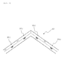
- Fig. 1 is a front perspective view illustrating a display device of an embodiment of the invention
- Fig. 2 is an exploded perspective view illustrating a configuration of a display panel assembly of the embodiment of the invention.
- a display device 100 a display panel assembly 200 which constitutes a display unit of the display device 100
- a front bezel 201 a liquid crystal cell 202 which displays a video picture thereon
- a light source 203 which causes light to be transmitted through the liquid crystal cell 202 from the rear side thereof
- a back chassis 204 a light guiding plate 205 which receives the light emitted from the light source 203 from one end surface so as to evenly brighten a screen
- an optical sheet 206 which diffuses and condenses the light guided by the light guiding plate 205
- a middle frame 207 which is positioned before the optical sheet 206
- a reflection sheet 208 which is positioned between the back chassis 204 and the light guiding plate 205.
- the front bezel 201 is formed by molding a resin material such as polystyrene.
- Fig. 3 is a schematic side cross-sectional view illustrating a molding die for the front bezel of the embodiment of the invention
- Fig. 4 is a schematic rear partially enlarged perspective view illustrating a material injection position of a front bezel unit of the embodiment of the invention.
- a plurality of material injection positions 201j, 201j, ... are provided near the rear surface side edge of the front bezel 201.
- the front bezel 201 is formed by hot runner molding that injects a material into a fixed die 800b and separates a molded product.
- the hot runner molding only the front bezel 201 as the molded product is discharged by suppressing the discharge of a sprue and a runner, whereby an extra material cost may be suppressed. Further, since the material injection positions 201j, 201j, ... are provided near the peripheral edge of the front bezel 201, it is possible to prevent the interference between the material injection positions 201j and components such as the liquid crystal cell 202 constituting the display panel assembly 200.
- the front bezel 201 serves as the front surface of the display panel assembly 200 and also serves as a front surface side outer casing of the display device 100, there is no need to provide a front cabinet constituting an additional front surface side outer casing and to provide a display device that decreases the thickness thereof and narrows the frame thereof.
- the material of the front bezel 201 of the invention is not limited to polystyrene, and a material which is generally called a resin may be appropriately used.
- the back chassis 204 is molded by a metal member such as a steel plate. Then, since the back chassis 204 serves as the rear surface of the display panel assembly 200 and also serves as a part of the rear surface side outer casing of the display device 100, there is no need to provide an additional back cabinet constituting the rear surface side outer casing and hence to provide a display device that further decreases the thickness thereof. Furthermore, the material of the back chassis 204 of the invention is not limited to the steel plate, and a material which is generally called metal may be appropriately used.
- the display panel assembly 200 is made by attaching various components including the liquid crystal cell 202 and the light source 203 to display a video picture into a space which is formed by assembling the front bezel 201 and the back chassis 204. Further, the liquid crystal cell 202 and a driving circuit board 202b are connected to each other through flexible printed interconnection boards 202c and 202c. Then, the light source 203 is disposed at the lower end inside the space of the display panel assembly 200, and the driving circuit board 202b is attached to the lower side of the rear surface of the back chassis 204 by screwing.
- the light source 203 and the driving circuit board 202b are disposed at one side of the display panel assembly 200, it is possible to decrease the thickness of the other side of the display panel assembly 200 and hence to further narrow the frame of the peripheral edge of the display unit. Furthermore, in the case of the embodiment, the thickness of the upper side of the display panel assembly 200 is decreased by integrating the light source 203 and the driving circuit board 202b at the lower side of the display panel assembly 200, but the invention is not limited to the above-described configuration. Those components may be integrated at any one side in the vertical and horizontal directions, and the integration position may be appropriately selected depending on the structure of the display device.
- the resinous front bezel 201 serves as the front cabinet of the related art and the metallic back chassis 204 serves as the back cabinet of the related art. Accordingly, it is possible to decrease the number of exterior components which is needed in the related art. In addition, it is possible to decrease the thickness and the weight of the display device and to narrow the frame of the peripheral edge of the display unit.
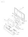
- FIG. 5 is a rear exploded perspective view illustrating a configuration of the display device of the embodiment of the invention.
- the above-described driving circuit board 202b is attached to the lower side of the rear surface of the display panel assembly 200, and a substrate attachment portion (not illustrated) is substantially formed at the center thereof by raising or bending.
- a control substrate 300 which includes a power supply unit and a control unit of the display device 100 is attached to the substrate attachment portion.
- the control substrate 300 may be one substrate or a plurality of substrates.
- a description will be continued on the assumption that the control substrate is formed as two substrates, that is, a substrate (hereinafter, simply referred to as a power circuit board) 302 which includes a power supply circuit for supplying a power to the display device 100 and a substrate (hereinafter, simply referred to as a control circuit board) 301 which includes a control circuit for controlling a signal input from the outside and performing a display on the liquid crystal cell 202 as the display unit of the display panel assembly 200.
- a cover member (hereinafter, referred to as a first cover member) 401 having a size of covering the power circuit board 302 and the control circuit board 301 attached to the substrate attachment portion of the back chassis 204 is attached thereto.
- Fig. 6 is a perspective view illustrating an inner surface of a first cover member of the embodiment of the invention.
- a partition rib 401 a which divides the power circuit board 302 and the control circuit board 301 is formed inside the first cover member 401. This is provided so as to prevent the breakage or the malfunction caused when the components or the wires of the control circuit board 301 contact the components of the high-voltage power circuit board 302.
- the method of attaching the power circuit board 302 and the control circuit board 301 is not limited to the configuration of the embodiment.
- the substrate attachment portion may be formed at the inner surface of the first cover member 401 and the control substrate 300 may be attached thereto.
- the power supply circuit and the control circuit are formed as different substrates, but the power supply circuit and the control circuit may be integrated into one substrate.
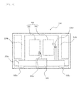
- Fig. 7 is a schematic rear transparent view of a display panel assembly of the embodiment of the invention
- Fig. 8 is a rear view of the display panel assembly of the embodiment of the invention.
- an LED substrate hereinafter, referred to as an LED substrate 203 having a plurality of LEDs arranged thereon is used as the light source 203 inside the display panel assembly 200, and the LED substrate 203 and the control circuit board 301 are connected to each other by a flexible flat cable 202d.
- the flexible flat cable 202d passes through a hole (hereinafter, referred to as an insertion hole) 204j which is formed in a rear surface 204a of the back chassis 204 so as to cause a wire to pass therethrough.
- the insertion hole 204j through which the end of the flexible flat cable 202d protrudes is formed in the rear surface 204a of the back chassis 204 in the vicinity of the control circuit board 301 attached through the flexible flat cable 202d connected to the LED substrate 203 between the back chassis 204 and the reflection sheet 208. Furthermore, the flexible flat cable 202d is disposed between the back chassis 204 and the reflection sheet 208 at the step of assembling the display panel assembly 200.
- a support plate 500 is attached so as to traverse a part of the driving circuit board 202b attached to the lower side of the rear surface of the display panel assembly 200.
- the support plate 500 is formed of metal, and is provided so as to detachably attach a stand 600 thereto by a user from the bottom surface of the display panel assembly 200. Also, it is possible to prevent an unnecessary radiation of a connection wire 202e which connects the driving circuit board 202b and the power circuit board 302 to each other.
- connection wire 202e it is possible to prevent an unnecessary radiation by connecting the connection wire 202e to the power circuit board 302 through a gap between the driving circuit board 202b and the support plate 500, and to reduce an operation and a member that coats the connection wire 202e by a tape having a high insulation property.
- the back chassis 204 is provided with steps 204k, 204k, ... which are continuously formed by drawing.
- the steps 204k, 204k, ... are respectively formed at the entire circumference of the back chassis 204 and positions which substantially trisect the back chassis 204.
- the steps 204k, 204k, ... reinforce the display panel assembly 200, and remove a gap between the rear surface 204a of the back chassis 204 and the first cover member 401 attached to the rear surface 204a so as to prevent the light emitted from the LED substrate 203 from leaking to the outside of the display device 100 from the substrate attachment portion and the like.
- Fig. 9 is a rear view of a display panel assembly of another embodiment of the invention. As illustrated in the drawing, it is possible to further improve the strength of the display panel assembly 200 by providing substantially triangular steps 204m and 204m.
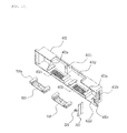
- Fig. 10 is an exploded perspective view illustrating an inner surface of a second cover member of the embodiment of the invention
- Fig. 11 is a partially enlarged perspective view illustrating the inner surface of the second cover member of the embodiment of the invention
- Fig. 12 is a schematic partially cross-sectional perspective view illustrating a connection position between a first cover member and the second cover member of the embodiment of the invention
- Fig. 13 is a schematic rear view illustrating the display device of the embodiment of the invention
- Fig. 14 is a schematic side cross-sectional view illustrating the second cover member of the embodiment of the invention
- Fig. 15 is a schematic rear transparent view of the display device of the embodiment of the invention.
- the second cover member 402 is provided with speaker attachment portions 402a and 402a, an operation portion 402b, an operation substrate attachment portion 402c, and a light receiving and emitting substrate attachment portion 402d.
- Speakers 700 and 700 are attached to the speaker attachment portions 402a and 402a formed in the second cover member 402 through dampers 700a, 700a, ..., and the bottom surface of the second cover member 402 is provided with output holes 402h and 402h which output a sound output from the speakers 700 and 700 to the outside of the display device 100.
- the sound output portion of the speaker 700 faces downward, but the output hole 402h is formed forward-slantingly at the bottom surface of the second cover member 402 so that the sound is output to the front side of the display device 1. For this reason, when attaching the second cover member 402 to the display device assembly 200, the bottom surface of the second cover member 402 is slightly inclined.
- a plurality of small holes 402e, 402e, ... are formed at the rear side of the speaker attachment portion 402a. Then, the first cover member 401 and the second cover member 402 are connected to each other, and a sound output from the speakers 700 and 700 attached to the speaker attachment portions 402a and 402a of the second cover member 402 is output through the inside of the first cover member 401, thereby improving the quality of the sound without additionally providing a speaker box. Further, it is possible to cause a heat generated inside the first cover member 401 and the second cover member 402 to dissipate through the small holes 402e, 402e, ... by the vibration of the speaker 700. Furthermore, a connection structure between the first cover member 401 and the second cover member 402 will be described later.
- a plurality of convex portions 402f, 402f, ... are formed in the upper portion of the second cover member 402.
- the convex portions 402f, 402f, ... are attached so as to contact the back chassis 204, and are provided so as to suppress an unpleasant sound such as chatter noise which is generated when the second cover member 402 interferes with the back chassis 204 by the vibration of the speakers 700 and 700.
- chatter noise may be suppressed without the non-woven cloth by adopting a contact structure using the plurality of convex portions 402f, 402f, ...
- the convex portion 402f for suppressing the chatter noise is formed only at the upper portion of the second cover member 402.
- the invention is not limited to the above-described configuration, and if necessary, the convex portion 402f may be formed at a position where the second cover member 402 and the back chassis 204 contact each other.
- one side surface of the second cover member 402 is integrated with the operation portion 402b having a plurality of pressing portions, and the inner surface of the operation portion 402b is provided with the operation substrate attachment portion 402c for attaching the operation substrate 303 provided with a plurality of switches. Then, the operation substrate 303 is attached to the operation substrate attachment portion 402c. Further, the second cover member 402 is provided with the light receiving and emitting substrate attachment portion 402d for attaching the light receiving and emitting substrate 304 provided with a light receiving portion and a light emitting portion. Then, the light receiving and emitting substrate 304 is attached to the light receiving and emitting substrate attachment portion 402d.
- the front bezel 201 which is present at a position facing the light receiving and emitting substrate 304 is provided with a light receiving guide portion 201 h which guides a signal of a remote controller for remotely controlling the display device 100 to the light receiving portion and a light emitting guide portion 201 i which guides the light of the light emitting portion for visually recognizing the state of the display device 100 to the outside.
- first cover member 401 and the second cover member 402 are connected to each other by being attached to the rear surface of the display panel assembly 200. That is, the lower side of the first cover member 401 is provided with a fastening boss 401c through which a screw is inserted, and the upper side of the second cover member 402 is provided with a connection boss 402i through which a screw is inserted while overlapping the fastening boss 401c.
- first cover member 401 and the second cover member 402 are attached to the rear surface of the display panel assembly 200, the fastening boss 401c and the connection boss 402i overlap each other, and then the bosses are screw-fastened to each other, thereby attaching the first cover member 401 and the second cover member 402 in a connected state.
- the display device 100 may be reinforced. Specifically, since the second cover member 402 substantially having the same width as that of the display panel assembly 200 is attached, the horizontal rigidity of the display device 100 may be obtained. Further, since the first cover member 401 and the second cover member 402 are connected to each other, the vertical rigidity of the display device 100 may be obtained.
- the back chassis 204 constituting the rear surface of the display panel assembly 200 by the same color as those of the first cover member 401 and the second cover member 402.
- black painting is desirable. This is because a part of the back chassis 204 becomes the rear surface exterior portion of the display device 100 along with the first cover member 401 and the second cover member 402.
- the back chassis 204 is painted in black, a heat dissipation effect for heat radiating components arranged on various substrates may be expected.
Landscapes
- Physics & Mathematics (AREA)
- Nonlinear Science (AREA)
- Engineering & Computer Science (AREA)
- Multimedia (AREA)
- Signal Processing (AREA)
- Mathematical Physics (AREA)
- Chemical & Material Sciences (AREA)
- Crystallography & Structural Chemistry (AREA)
- General Physics & Mathematics (AREA)
- Optics & Photonics (AREA)
- Devices For Indicating Variable Information By Combining Individual Elements (AREA)
- Liquid Crystal (AREA)
Applications Claiming Priority (2)
| Application Number | Priority Date | Filing Date | Title |
|---|---|---|---|
| JP2012170185 | 2012-07-31 | ||
| JP2012004667U JP3179027U (ja) | 2012-07-31 | 2012-07-31 | 表示装置 |
Publications (1)
| Publication Number | Publication Date |
|---|---|
| EP2693263A1 true EP2693263A1 (de) | 2014-02-05 |
Family
ID=47257454
Family Applications (1)
| Application Number | Title | Priority Date | Filing Date |
|---|---|---|---|
| EP12190521.0A Withdrawn EP2693263A1 (de) | 2012-07-31 | 2012-10-30 | Anzeigevorrichtung |
Country Status (2)
| Country | Link |
|---|---|
| EP (1) | EP2693263A1 (de) |
| CN (1) | CN202975526U (de) |
Cited By (2)
| Publication number | Priority date | Publication date | Assignee | Title |
|---|---|---|---|---|
| US20200204893A1 (en) * | 2017-08-03 | 2020-06-25 | Lg Display Co., Ltd. | Display apparatus |
| CN113766388A (zh) * | 2020-06-05 | 2021-12-07 | 船井电机株式会社 | 显示装置和用于显示装置的扬声器 |
Families Citing this family (1)
| Publication number | Priority date | Publication date | Assignee | Title |
|---|---|---|---|---|
| CN104269109B (zh) | 2014-09-25 | 2017-02-15 | 高创(苏州)电子有限公司 | 一种显示装置后壳和显示装置 |
Citations (5)
| Publication number | Priority date | Publication date | Assignee | Title |
|---|---|---|---|---|
| JP2000315054A (ja) | 1999-04-30 | 2000-11-14 | Citizen Watch Co Ltd | 液晶表示装置 |
| EP1494467A1 (de) * | 2003-07-02 | 2005-01-05 | Pioneer Corporation | Flache Anzeigevorrichtung |
| JP2007163861A (ja) | 2005-12-14 | 2007-06-28 | Orion Denki Kk | 表示装置 |
| JP2009171520A (ja) * | 2008-01-21 | 2009-07-30 | Funai Electric Co Ltd | 薄型表示装置 |
| US20100033641A1 (en) * | 2008-08-08 | 2010-02-11 | Panasonic Corporation | Image display device |
-
2012
- 2012-10-30 EP EP12190521.0A patent/EP2693263A1/de not_active Withdrawn
- 2012-10-31 CN CN2012205755907U patent/CN202975526U/zh not_active Expired - Fee Related
Patent Citations (5)
| Publication number | Priority date | Publication date | Assignee | Title |
|---|---|---|---|---|
| JP2000315054A (ja) | 1999-04-30 | 2000-11-14 | Citizen Watch Co Ltd | 液晶表示装置 |
| EP1494467A1 (de) * | 2003-07-02 | 2005-01-05 | Pioneer Corporation | Flache Anzeigevorrichtung |
| JP2007163861A (ja) | 2005-12-14 | 2007-06-28 | Orion Denki Kk | 表示装置 |
| JP2009171520A (ja) * | 2008-01-21 | 2009-07-30 | Funai Electric Co Ltd | 薄型表示装置 |
| US20100033641A1 (en) * | 2008-08-08 | 2010-02-11 | Panasonic Corporation | Image display device |
Cited By (4)
| Publication number | Priority date | Publication date | Assignee | Title |
|---|---|---|---|---|
| US20200204893A1 (en) * | 2017-08-03 | 2020-06-25 | Lg Display Co., Ltd. | Display apparatus |
| US10966009B2 (en) * | 2017-08-03 | 2021-03-30 | Lg Display Co., Ltd. | Display apparatus |
| CN113766388A (zh) * | 2020-06-05 | 2021-12-07 | 船井电机株式会社 | 显示装置和用于显示装置的扬声器 |
| CN113766388B (zh) * | 2020-06-05 | 2024-05-24 | 船井电机株式会社 | 显示装置和用于显示装置的扬声器 |
Also Published As
| Publication number | Publication date |
|---|---|
| CN202975526U (zh) | 2013-06-05 |
Similar Documents
| Publication | Publication Date | Title |
|---|---|---|
| US7760491B2 (en) | Display apparatus | |
| US7889484B2 (en) | Display apparatus | |
| US7697272B2 (en) | Display apparatus | |
| US7663870B2 (en) | Display apparatus | |
| JP5496542B2 (ja) | 画像表示装置 | |
| KR101621794B1 (ko) | 디스플레이장치 | |
| EP4283982A2 (de) | Anzeigevorrichtung | |
| JP2006106618A (ja) | 表示装置 | |
| KR20090080009A (ko) | 패널형 디스플레이장치 | |
| EP4509910A2 (de) | Anzeigevorrichtung | |
| JP5519758B2 (ja) | 液晶表示装置 | |
| EP2693263A1 (de) | Anzeigevorrichtung | |
| KR20180067143A (ko) | 디스플레이 장치 | |
| US20140036178A1 (en) | Display device | |
| EP2790401A1 (de) | Anzeigegerät | |
| CN107277407A (zh) | 液晶电视机 | |
| KR20110035649A (ko) | 디스플레이 장치 | |
| CN206948482U (zh) | 液晶电视机 | |
| JP2014029421A (ja) | 表示装置 | |
| JP3179027U (ja) | 表示装置 | |
| KR20100122305A (ko) | 디스플레이 기기 | |
| JP2015011040A (ja) | 液晶表示装置 | |
| KR101801094B1 (ko) | 디스플레이장치 | |
| JPWO2019043789A1 (ja) | 操作機器 | |
| KR20110017162A (ko) | 디스플레이 장치 |
Legal Events
| Date | Code | Title | Description |
|---|---|---|---|
| AK | Designated contracting states |
Kind code of ref document: A1 Designated state(s): AL AT BE BG CH CY CZ DE DK EE ES FI FR GB GR HR HU IE IS IT LI LT LU LV MC MK MT NL NO PL PT RO RS SE SI SK SM TR |
|
| AX | Request for extension of the european patent |
Extension state: BA ME |
|
| PUAI | Public reference made under article 153(3) epc to a published international application that has entered the european phase |
Free format text: ORIGINAL CODE: 0009012 |
|
| STAA | Information on the status of an ep patent application or granted ep patent |
Free format text: STATUS: THE APPLICATION IS DEEMED TO BE WITHDRAWN |
|
| 18D | Application deemed to be withdrawn |
Effective date: 20140806 |