EP2695207B1 - Puce semi-conductrice optoélectronique - Google Patents
Puce semi-conductrice optoélectronique Download PDFInfo
- Publication number
- EP2695207B1 EP2695207B1 EP12708853.2A EP12708853A EP2695207B1 EP 2695207 B1 EP2695207 B1 EP 2695207B1 EP 12708853 A EP12708853 A EP 12708853A EP 2695207 B1 EP2695207 B1 EP 2695207B1
- Authority
- EP
- European Patent Office
- Prior art keywords
- layer
- semiconductor chip
- electrical contact
- semiconductor
- chip according
- Prior art date
- Legal status (The legal status is an assumption and is not a legal conclusion. Google has not performed a legal analysis and makes no representation as to the accuracy of the status listed.)
- Active
Links
Images






Classifications
-
- H—ELECTRICITY
- H10—SEMICONDUCTOR DEVICES; ELECTRIC SOLID-STATE DEVICES NOT OTHERWISE PROVIDED FOR
- H10H—INORGANIC LIGHT-EMITTING SEMICONDUCTOR DEVICES HAVING POTENTIAL BARRIERS
- H10H20/00—Individual inorganic light-emitting semiconductor devices having potential barriers, e.g. light-emitting diodes [LED]
- H10H20/80—Constructional details
- H10H20/85—Packages
- H10H20/855—Optical field-shaping means, e.g. lenses
- H10H20/856—Reflecting means
-
- H—ELECTRICITY
- H10—SEMICONDUCTOR DEVICES; ELECTRIC SOLID-STATE DEVICES NOT OTHERWISE PROVIDED FOR
- H10H—INORGANIC LIGHT-EMITTING SEMICONDUCTOR DEVICES HAVING POTENTIAL BARRIERS
- H10H20/00—Individual inorganic light-emitting semiconductor devices having potential barriers, e.g. light-emitting diodes [LED]
- H10H20/80—Constructional details
- H10H20/83—Electrodes
- H10H20/831—Electrodes characterised by their shape
-
- H—ELECTRICITY
- H10—SEMICONDUCTOR DEVICES; ELECTRIC SOLID-STATE DEVICES NOT OTHERWISE PROVIDED FOR
- H10H—INORGANIC LIGHT-EMITTING SEMICONDUCTOR DEVICES HAVING POTENTIAL BARRIERS
- H10H20/00—Individual inorganic light-emitting semiconductor devices having potential barriers, e.g. light-emitting diodes [LED]
- H10H20/80—Constructional details
- H10H20/83—Electrodes
- H10H20/832—Electrodes characterised by their material
- H10H20/835—Reflective materials
-
- H—ELECTRICITY
- H10—SEMICONDUCTOR DEVICES; ELECTRIC SOLID-STATE DEVICES NOT OTHERWISE PROVIDED FOR
- H10H—INORGANIC LIGHT-EMITTING SEMICONDUCTOR DEVICES HAVING POTENTIAL BARRIERS
- H10H20/00—Individual inorganic light-emitting semiconductor devices having potential barriers, e.g. light-emitting diodes [LED]
- H10H20/80—Constructional details
- H10H20/84—Coatings, e.g. passivation layers or antireflective coatings
-
- H—ELECTRICITY
- H10—SEMICONDUCTOR DEVICES; ELECTRIC SOLID-STATE DEVICES NOT OTHERWISE PROVIDED FOR
- H10H—INORGANIC LIGHT-EMITTING SEMICONDUCTOR DEVICES HAVING POTENTIAL BARRIERS
- H10H20/00—Individual inorganic light-emitting semiconductor devices having potential barriers, e.g. light-emitting diodes [LED]
- H10H20/80—Constructional details
- H10H20/85—Packages
- H10H20/852—Encapsulations
-
- H—ELECTRICITY
- H10—SEMICONDUCTOR DEVICES; ELECTRIC SOLID-STATE DEVICES NOT OTHERWISE PROVIDED FOR
- H10H—INORGANIC LIGHT-EMITTING SEMICONDUCTOR DEVICES HAVING POTENTIAL BARRIERS
- H10H20/00—Individual inorganic light-emitting semiconductor devices having potential barriers, e.g. light-emitting diodes [LED]
- H10H20/01—Manufacture or treatment
- H10H20/011—Manufacture or treatment of bodies, e.g. forming semiconductor layers
- H10H20/018—Bonding of wafers
-
- H—ELECTRICITY
- H10—SEMICONDUCTOR DEVICES; ELECTRIC SOLID-STATE DEVICES NOT OTHERWISE PROVIDED FOR
- H10H—INORGANIC LIGHT-EMITTING SEMICONDUCTOR DEVICES HAVING POTENTIAL BARRIERS
- H10H20/00—Individual inorganic light-emitting semiconductor devices having potential barriers, e.g. light-emitting diodes [LED]
- H10H20/01—Manufacture or treatment
- H10H20/032—Manufacture or treatment of electrodes
-
- H—ELECTRICITY
- H10—SEMICONDUCTOR DEVICES; ELECTRIC SOLID-STATE DEVICES NOT OTHERWISE PROVIDED FOR
- H10H—INORGANIC LIGHT-EMITTING SEMICONDUCTOR DEVICES HAVING POTENTIAL BARRIERS
- H10H20/00—Individual inorganic light-emitting semiconductor devices having potential barriers, e.g. light-emitting diodes [LED]
- H10H20/80—Constructional details
- H10H20/81—Bodies
- H10H20/819—Bodies characterised by their shape, e.g. curved or truncated substrates
- H10H20/82—Roughened surfaces, e.g. at the interface between epitaxial layers
-
- H—ELECTRICITY
- H10—SEMICONDUCTOR DEVICES; ELECTRIC SOLID-STATE DEVICES NOT OTHERWISE PROVIDED FOR
- H10H—INORGANIC LIGHT-EMITTING SEMICONDUCTOR DEVICES HAVING POTENTIAL BARRIERS
- H10H20/00—Individual inorganic light-emitting semiconductor devices having potential barriers, e.g. light-emitting diodes [LED]
- H10H20/80—Constructional details
- H10H20/83—Electrodes
- H10H20/831—Electrodes characterised by their shape
- H10H20/8312—Electrodes characterised by their shape extending at least partially through the bodies
-
- H—ELECTRICITY
- H10—SEMICONDUCTOR DEVICES; ELECTRIC SOLID-STATE DEVICES NOT OTHERWISE PROVIDED FOR
- H10H—INORGANIC LIGHT-EMITTING SEMICONDUCTOR DEVICES HAVING POTENTIAL BARRIERS
- H10H20/00—Individual inorganic light-emitting semiconductor devices having potential barriers, e.g. light-emitting diodes [LED]
- H10H20/80—Constructional details
- H10H20/85—Packages
- H10H20/852—Encapsulations
- H10H20/853—Encapsulations characterised by their shape
-
- H—ELECTRICITY
- H10—SEMICONDUCTOR DEVICES; ELECTRIC SOLID-STATE DEVICES NOT OTHERWISE PROVIDED FOR
- H10H—INORGANIC LIGHT-EMITTING SEMICONDUCTOR DEVICES HAVING POTENTIAL BARRIERS
- H10H20/00—Individual inorganic light-emitting semiconductor devices having potential barriers, e.g. light-emitting diodes [LED]
- H10H20/80—Constructional details
- H10H20/85—Packages
- H10H20/852—Encapsulations
- H10H20/854—Encapsulations characterised by their material, e.g. epoxy or silicone resins
-
- H—ELECTRICITY
- H10—SEMICONDUCTOR DEVICES; ELECTRIC SOLID-STATE DEVICES NOT OTHERWISE PROVIDED FOR
- H10H—INORGANIC LIGHT-EMITTING SEMICONDUCTOR DEVICES HAVING POTENTIAL BARRIERS
- H10H20/00—Individual inorganic light-emitting semiconductor devices having potential barriers, e.g. light-emitting diodes [LED]
- H10H20/80—Constructional details
- H10H20/85—Packages
- H10H20/857—Interconnections, e.g. lead-frames, bond wires or solder balls
Definitions
- the invention relates to an optoelectronic semiconductor chip.
- an optoelectronic semiconductor chip in which a first and a second electrical contact layer are arranged between the semiconductor layer sequence and the carrier substrate.
- the first and the second electrical contact layer are insulated from each other by means of an electrically insulating layer.
- a mirror layer may adjoin the semiconductor layer sequence on a side facing the carrier substrate in order to deflect the radiation emitted by the active zone in the direction of the carrier substrate to a radiation coupling-out surface opposite the carrier substrate.
- DE 10 2009 022 966 A1 and DE 10 2008 030 584 A1 disclose similar optoelectronic semiconductor chips.
- the risk may exist that moisture is transported from the edges of the semiconductor chip through the electrically insulating layer into the region of the mirror layer, which would result in degradation of the mirror layer and thus a reduction in the radiation yield.
- the invention has for its object to provide an improved optoelectronic semiconductor chip, wherein the Mirror layer is effectively protected from the ingress of moisture and at the same time an efficient electrical contacting of the semiconductor chip is achieved with relatively little manufacturing effort.
- the optoelectronic semiconductor chip comprises a semiconductor layer sequence which has a first semiconductor region of a first conductivity type, a second semiconductor region of a second conductivity type and an active zone arranged between the first and the second semiconductor region.
- the optoelectronic semiconductor chip comprises a carrier substrate, wherein the semiconductor layer sequence has a first main area facing the carrier substrate and an opposite second main area.
- a first electrical contact layer and a second electrical contact layer are arranged at least in regions between the carrier substrate and the first main surface of the semiconductor layer sequence, wherein the second electrical contact layer is guided through an opening in the first semiconductor region and the active zone into the second semiconductor region.
- the first and second electrical contact layers are insulated from each other by an electrically insulating layer.
- a mirror layer is arranged between the semiconductor layer sequence and the carrier substrate.
- the mirror layer can in particular adjoin the semiconductor layer sequence on the first main surface. Radiation, which is emitted from the active zone in the direction of the carrier substrate, is advantageously reflected by the mirror layer to the second main area of the semiconductor layer sequence serving as the radiation coupling-out area.
- the mirror layer is in particular adjacent to partial regions of the first electrical contact layer and to partial regions of the electrically insulating layer, wherein the carrier substrate facing the interface of the mirror layer is covered by the first electrical contact layer.
- the optoelectronic semiconductor chip according to the present invention comprises a transparent encapsulation layer covering side surfaces of the semiconductor layer sequence, side surfaces of the mirror layer, and side surfaces of the electrically insulating layer facing the side surfaces of the semiconductor chip. Furthermore, the transparent encapsulation layer completely covers the semiconductor layer sequence. The side surfaces of the mirror layer are also surrounded on all sides by the transparent encapsulation layer.
- the transparent encapsulation layer covers the side surfaces of the semiconductor layer sequence and the mirror layer protects the mirror layer from the penetration of moisture.
- This protective effect of the transparent encapsulation layer is further improved in that the transparent encapsulation layer also covers the side surfaces of the electrically insulating layer facing the side surfaces of the semiconductor chip. In this way, in particular the penetration of moisture into the electrically insulating layer is prevented, thereby reducing the risk that moisture will pass through the electrically insulating layer all the way to the surface Mirror layer spreads.
- the electrically insulating layer preferably does not adjoin an ambient medium of the optoelectronic semiconductor chip at any point. Thus, it is advantageously ensured that moisture can not penetrate from the outside into the electrically insulating layer and can propagate in the layer system of the semiconductor chip.
- the transparent encapsulation layer preferably contains or consists of an aluminum oxide such as Al 2 O 3 or a silicon oxide such as SiO 2 .
- the transparent encapsulant layer comprises an AlD layer, i. an atomic layer deposition (ALD) layer.
- the transparent encapsulation layer has a spin-on glass.
- An ALD layer or a spin-on glass is advantageously distinguished by a low defect density and offers good protection against the penetration of moisture.
- the application of the transparent encapsulation layer by means of ALD or as spin-on glass also has the advantage that the transparent encapsulation view can be introduced into small intermediate spaces.
- the mirror layer has a smaller lateral extent than the semiconductor layer sequence, and partial regions of the transparent encapsulation layer extend below the semiconductor layer sequence. In this way, a particularly good protection of the mirror layer from oxidation and / or the ingress of moisture is achieved.
- the Semiconductor layer sequence on all side surfaces on a supernatant on the mirror layer.
- a gap which is formed between the semiconductor layer sequence and a layer sequence applied to the carrier substrate, advantageously adjoins the side surfaces of the mirror layer. This gap is advantageously filled by the transparent encapsulation layer.
- the second main surface of the semiconductor layer sequence which serves in particular as a radiation exit surface, is completely covered by the transparent encapsulation layer.
- the semiconductor layer sequence is complete, i. including the side surfaces covered by the transparent encapsulation layer.
- the semiconductor layer sequence has a mesa structure, wherein the first and the second electrical contact layer extend into regions of the semiconductor chip arranged laterally next to the mesa structure.
- the transparent encapsulation layer preferably has, in addition to the mesa structure, an opening in which a connection contact for the first electrical contact layer is arranged.
- the connection contact is advantageously arranged next to the semiconductor layer sequence, so that, in particular, a second main surface of the semiconductor layer sequence acting as a radiation exit surface is free of connection contacts. This has the advantage that the radiation exit surface is not shadowed by the connection contact and thus the efficiency of the Semiconductor chips increased.
- the connection contact is preferably arranged outside the center of the semiconductor chip, in particular in a corner of the semiconductor chip.
- the first electrical contact layer is advantageously used for electrical contacting of the semiconductor chip and for protecting the mirror layer from corrosion.
- at least part of the substrate surface facing the interface of the mirror layer is covered by the first electrical contact layer.
- the first electrical contact layer preferably contains or consists of gold, titanium, chromium, platinum, titanium nitride, titanium tungsten nitride or nickel. These materials are characterized on the one hand by a good electrical conductivity and on the other by their suitability as a diffusion barrier.
- the first electrical contact layer may comprise a plurality of sub-layers, which preferably each contain at least one of these materials.
- the mirror layer preferably contains or consists of silver, aluminum or a silver or aluminum alloy.
- Silver and aluminum are characterized by a high reflection in the visible spectral range. Furthermore, these materials have good electrical conductivity and form a metal-semiconductor contact with low contact resistance. This is advantageous since the mirror layer advantageously adjoins the semiconductor layer sequence and in this way electrically conductively connects the first semiconductor region to the first electrical contact layer.
- the second electrical contact layer like the mirror layer, preferably contains or consists of silver, aluminum or one or a silver or aluminum alloy. A high reflection in the visible spectral range and a good electrical conductivity are advantageous for the second electrical contact layer, since the second electrical contact layer is at least partially adjacent to the semiconductor layer sequence and thus electrically contacted the second semiconductor region.
- the electrically insulating layer which isolates the first electrical contact layer and the second electrical contact layer from one another, preferably contains a silicon oxide, a silicon nitride, a silicon oxynitride or an aluminum oxide.
- the first semiconductor region is a p-type semiconductor region and the second semiconductor region is an n-type semiconductor region.
- the mirror layer adjoins the p-type semiconductor region, and the second electrical contact layer is led through the aperture into the n-type semiconductor region.
- the p-type semiconductor region faces the carrier substrate and the n-type semiconductor region faces the second main surface of the semiconductor layer sequence serving as the radiation exit surface.
- the semiconductor layer sequence of the optoelectronic semiconductor chip has no growth substrate.
- the semiconductor chip is a so-called thin-film light-emitting diode chip in which the chip used for the epitaxial growth of the semiconductor layer sequence Waxing substrate was detached after connecting the semiconductor layer sequence with the carrier substrate.
- the semiconductor chip is preferably connected to the carrier substrate by means of a solder layer.
- the semiconductor chip may be connected to the carrier substrate at the side opposite the original growth substrate.
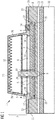
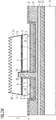
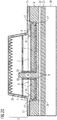
- FIG. 1 schematically illustrated in cross section optoelectronic semiconductor chip 1 contains a Semiconductor layer sequence 2, which has a first semiconductor region 3 of a first conductivity type and a second semiconductor region 5 of a second conductivity type.
- the first semiconductor region 3 is a p-type semiconductor region and the second semiconductor region 5 is an n-type semiconductor region.
- an active zone 4 is arranged between the first semiconductor region 3 and the second semiconductor region 5.
- the active zone 4 of the optoelectronic semiconductor chip 1 may in particular be an active zone suitable for the emission of radiation.
- the optoelectronic semiconductor chip 1 is a light-emitting diode, in particular an LED.
- the active zone 4 is a radiation-detecting layer, wherein the optoelectronic semiconductor chip 1 in this case is a detector component.
- the active zone 4 may be formed, for example, as a pn junction, as a double heterostructure, as a single quantum well structure or a multiple quantum well structure.
- the semiconductor layer sequence 2 of the semiconductor chip 1 is preferably based on a III-V compound semiconductor material, in particular on an arsenide, nitride or phosphide compound semiconductor material.
- the semiconductor layer sequence 2 In x Al y Ga 1-xy N, In x Al y Ga 1-xy P or In x Al y Ga 1-xy As, each with 0 ⁇ x ⁇ 1, 0 ⁇ y ⁇ 1 and x + y ⁇ 1.
- the III-V compound semiconductor material does not necessarily have to have a mathematically exact composition according to one of the above formulas. Rather, it may have one or more dopants as well as additional ingredients that enhance the physical properties of the material in the not change.
- the above formulas contain only the essential constituents of the crystal lattice, even if these may be partially replaced by small amounts of other substances.
- the semiconductor chip 1 is connected to a connection layer 21, which may in particular be a solder layer made of a metal or a metal alloy, with a carrier substrate 10.
- the semiconductor chip 1 has a first electrical contact layer 7 and a second electrical contact layer 8.
- the first electrical contact layer 7 is electrically conductively connected to the first semiconductor region 3 and the second electrical contact layer 8 is electrically conductively connected to the second semiconductor region 5.
- Both the first electrical contact layer 7 and the second electrical contact layer 8 are arranged at least in regions between a first main surface 11 of the semiconductor layer sequence 2 facing the carrier substrate 10 and the carrier substrate 10.
- the first electrical contact layer 7 and the second electrical contact layer 8 are electrically insulated from one another by means of an electrically insulating layer 9.
- the electrically insulating layer 9 preferably contains or consists of a silicon oxide, a silicon nitride, a silicon oxynitride, an aluminum oxide. Alternatively, the electrically insulating layer 9 may also contain other oxides or nitrides.
- the second main surface 12 of the semiconductor layer sequence 2 opposite the carrier substrate 10 serves as Radiation decoupling surface of the optoelectronic semiconductor chip 1 and is advantageously free of electrical contact layers.
- the second main surface 12 may be provided with a decoupling structure 23 or a roughening.
- a mirror layer 6 is arranged between the semiconductor layer sequence 2 and the carrier substrate 10.
- the mirror layer 6 is arranged downstream of the first semiconductor region 3 on the side facing the carrier substrate 10 and can, in particular, adjoin the first main surface 11 of the semiconductor layer sequence 2.
- an intermediate layer is arranged between the first semiconductor region 3 and the mirror layer 6, for example a thin adhesion promoter layer.
- the mirror layer 6 contains in particular silver, aluminum or a metal alloy with silver or aluminum. These materials are characterized by a high reflectivity in the visible spectral range and a good electrical conductivity.
- the mirror layer 6 has, on the one hand, the function of reflecting radiation emitted by the active zone 4 in the direction of the carrier substrate 10 to the radiation coupling-out surface 12. Furthermore, the mirror layer 6 also serves for electrical contacting of the first semiconductor region 3. In particular, the mirror layer 6 adjoins the first electrical contact layer 7 on the side facing the carrier substrate 10 and is thus electrically conductively connected to the first electrical contact layer 7.
- the first electrical contact layer 7 preferably covers the carrier substrate 10 facing the interface of Mirror layer.
- the first electrical contact layer 7 preferably contains or consists of gold, titanium, chromium, platinum, titanium nitride, titanium tungsten nitride or nickel. These materials are characterized by being electrically conductive and also chemically inert. In this way, the mirror layer 6 is advantageously protected from corrosion in the areas in which it is covered by the first electrical contact layer 7.
- the second electrical contact layer 8 is electrically conductively connected to the second semiconductor region 5 through an opening 18 which extends through the first semiconductor region 3 and the active zone 4. In the region of the breakdown 18, the active zone 4, the first semiconductor region 3, the mirror layer 6 and the first electrical contact layer 7 are insulated from the second electrical contact layer 8 by means of the electrically insulating layer 9 or passivated regions 20 of the semiconductor layer sequence 2.
- the second electrical contact layer 8 functions in the regions in which it directly adjoins the semiconductor layer sequence 2, advantageously not only as a contact layer but also as a reflective layer, which reflects radiation toward the second main surface 12 of the semiconductor layer sequence 2 serving as the radiation exit surface.
- the second electrical contact layer 8 therefore advantageously has a metal or a metal alloy with a high reflectivity, in particular silver, aluminum or an alloy with silver or aluminum.
- the side surfaces 26 of the semiconductor layer sequence 2 and the side surfaces 16 of the Mirror layer 6 of an electrically insulating transparent encapsulation layer 13 covered.
- the encapsulation layer 13 has, on the one hand, the function of protecting the mirror layer 6 from corrosion.
- the mirror layer 6 is protected by the encapsulation layer 13 from oxidation or the ingress of moisture.
- the side surfaces 16 of the mirror layer 6 are surrounded on all sides by the encapsulation layer 13, so that the mirror layer 6 is not directly adjacent to the surrounding medium at any point.
- the transparent encapsulation layer 13 also covers the side surfaces 17 of the first contact layer 7 and the side surfaces 19 of the electrically insulating layer 9 facing the side surfaces 15 of the semiconductor chip 1. In this way, penetration of moisture into the electrically insulating layer 9 is prevented in particular.
- the electrically insulating layer 9 at no point adjoins an ambient medium of the semiconductor chip 1.
- the transparent encapsulation layer 13 is preferably an aluminum oxide layer, in particular an Al 2 O 3 layer, or a silicon oxide layer, in particular an SiO 2 layer.
- the transparent encapsulation layer is advantageously deposited by means of atomic layer deposition or as spin-on glass.
- Such a silicon oxide layer deposited by means of ALD or as a spin-on glass advantageously has a high resistance to corrosion and the penetration of moisture.
- the mirror layer 6 has a smaller lateral extent than the Semiconductor layer sequence 2, so that portions of the transparent encapsulation layer 13 extend below the semiconductor layer sequence 2.
- the side surfaces 16 of the mirror layer 6 are advantageously spaced from the side surfaces 26 of the semiconductor layer sequence 2 in this embodiment.
- the distance between the side surfaces 26 of the semiconductor layer sequence 2 and the side surfaces 16 of the mirror layer 6 is preferably between 0.5 ⁇ m and 5 ⁇ m, particularly preferably about 3 ⁇ m. In this way, the mirror layer 6 is particularly effectively protected.
- by producing the transparent encapsulation layer 13 by means of atomic layer deposition it is possible to deposit the transparent encapsulation layer 13 in such a way that it fills the gap between the semiconductor layer sequence 2 and the mirror layer 6.
- the transparent encapsulation layer 13 advantageously also covers the side surfaces 26 and the second main surface 12 of the semiconductor layer sequence 2 serving as the radiation exit surface.
- the semiconductor layer sequence 2 is thus advantageously completely covered by the transparent encapsulation layer 13.
- fine cracks which may be present on the surfaces of the semiconductor layer sequence 2 can be closed by the transparent encapsulation layer 13.
- the complete encapsulation of the semiconductor chip sequence 2 is therefore advantageous for the long-term stability of the semiconductor chip.
- the semiconductor layer sequence 2 has a mesa structure, wherein the first electrical contact layer 7 and the second electrical contact layer 8 extend laterally next to the mesa structure.
- the transparent Encapsulation layer 13 has, in addition to the mesa structure, an opening in which a connection contact 14 is arranged, which is connected to the first electrical contact layer.
- the connection contact 14 may in particular be a bonding pad, which is provided for connecting a bonding wire.
- connection contact 14 is preferably arranged outside the center of the semiconductor chip 1, in particular in the region of a corner of the semiconductor chip 1.
- the semiconductor chip 1 When the semiconductor chip 1 is viewed from above, essentially only the second electrical contact layer 8, which advantageously contains a highly reflective metal such as, for example, Ag or Al, is advantageously visible through the transparent encapsulation layer 13 in addition to the semiconductor layer sequence 2 structured as a mesa. Only in a small area around the terminal contact 14 areas of the first electrical contact layer 7 are visible, which may contain a less reflective material such as platinum.
- a highly reflective metal such as, for example, Ag or Al
- the second electrical contact layer 8 is electrically connectable from the outside, for example via the rear side of the semiconductor chip 1, in particular via an electrically conductive carrier substrate 10 and the solder layer 21. Between the solder layer 21 and the second electrical contact layer 8, a barrier layer 22 may be arranged, which in particular prevents diffusion of constituents of the solder layer 21 into the second electrical contact layer 8 and vice versa.
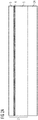
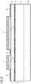
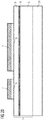
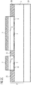
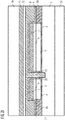
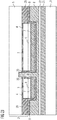
- FIGS. 2A to 2O is an embodiment of a method for producing the optoelectronic semiconductor chips described.
- the above-described advantageous embodiments of individual components of the optoelectronic semiconductor chip apply in the same way to the method described below and vice versa.
- the semiconductor layer sequence 2 which comprises the first semiconductor region 3, the active zone 4 and the second semiconductor region 5, has been grown on a growth substrate 24.
- the growth preferably takes place epitaxially, in particular by means of MOVPE.
- the semiconductor layer sequence 2 may include, for example, nitride compound semiconductor materials, and the growth substrate 24 may be a sapphire substrate.
- the first semiconductor region 3 is preferably a p-type semiconductor region, and the second semiconductor region 5 is preferably an n-type semiconductor region.
- an oxide layer 25 for example a silicon oxide layer, has been applied to the second semiconductor region 5.
- the oxide layer 25 serves to protect the first semiconductor region 3 during subsequent photolithographic and etching processes.
- the oxide layer was patterned, for example, photolithographically. Furthermore, the mirror layer 6 and the first electrical contact layer 7 were applied and lifted by lift-off technique of the still covered with the oxide layer 25 areas. Advantageously, therefore, the mirror layer 6 and the first electrical contact layer are patterned in the same process step.
- the mirror layer 6 contains in particular silver, aluminum or a metal alloy with silver or aluminum.
- the first electrical contact layer 7 covers the surface of the mirror layer 6 and in this way on the one hand establishes the electrical connection to the first semiconductor region 3, and on the other hand serves as an encapsulation for the material of the mirror layer 6.
- the first electrical contact layer 7 can in particular be gold, titanium , Chromium, platinum, titanium nitride, titanium tungsten nitride or nickel, or consist thereof. It is also possible for the first electrical contact layer 7 to comprise a plurality of partial layers. By way of example, the first electrical contact layer 7 may have a Ti / Pt / Au / Cr layer sequence.
- the p-type semiconductor region 3 has been passivated in areas 20 which are arranged between and outside the areas of the semiconductor layer sequence 2 covered by the mirror layer 6 and the first electrical contact layer 7.
- the passivated regions 20 can be produced, for example, by bombardment of the p-doped semiconductor material 3 with argon ions.
- the passivated regions 20 extend into the active layer 4, so that the pn junction is severed by the electrically insulating passivated regions 20.
- the structure prepared in this way was used in the in Figure 2F shown intermediate step applied an electrically insulating layer 9.
- the electrically insulating layer 9 may in particular be a silicon oxide or a silicon nitride layer.
- an opening 18 in the electrically insulating layer 9 and the semiconductor layer sequence 2 was generated.
- the aperture 18 is generated, for example, by photolithography and reactive ion etching.
- the breakdown 18 extends through the passivated regions 20 of the first semiconductor region 3 and the active layer 4 into the second semiconductor region 5.
- the second electrical contact layer 8 preferably contains silver, aluminum or an alloy with silver or aluminum.
- the second electrical contact layer 8 is used for electrical contacting of the second semiconductor region 5, which may in particular be an n-type semiconductor region.
- the second electrical contact layer 8 extends through the opening 18 into the second semiconductor region 5.
- the semiconductor chip has been connected to a carrier substrate 10 at a side remote from the growth substrate 24 by means of a solder layer 21.
- a barrier layer 22 is preferably applied to the second electrical contact layer 8, preferably around the silver or Aluminum-containing second electrical contact layer 8 to protect against diffusion of components of the solder layer 21.
- the solder layer 21 may in particular contain AuSn.
- the barrier layer 22 may include, for example, TiWN.
- the carrier substrate 10 is preferably an electrically conductive substrate, for example a doped semiconductor wafer made of silicon or germanium. Alternatively, the carrier substrate 10 may also be formed by an electrodeposited metal layer.
- the growth substrate 24 has been detached from the semiconductor chip.
- the semiconductor chip is shown rotated by 180 ° in comparison to the previous figures, since now the carrier substrate 10 opposite the original growth substrate acts as the sole carrier of the semiconductor chip.
- the growth substrate in particular a sapphire substrate, can be detached from the semiconductor layer sequence 2, for example, by means of a laser lift-off process.
- the main surface 12 of the semiconductor layer sequence 2, from which the growth substrate 24 was peeled off, was used in the case of FIG Figure 2K illustrated intermediate step provided with a coupling-out structure 23, for example by etching with KOH. This is advantageous since the second main surface 12 of the semiconductor layer sequence 2 in the finished optoelectronic semiconductor chip serves as a radiation output surface.
- the semiconductor layer sequence 2 was provided with a mesa structure.
- the semiconductor layer sequence 2 has been completely removed in the edge regions of the semiconductor chip in order to to produce a semiconductor layer sequence 2 having a desired shape and size.
- the structuring is preferably carried out by photolithography, it being possible to use, for example, H 3 PO 4 as etchant and SiO 2 as mask.
- the semiconductor layer sequence 2 has been removed in such a way that, in addition to the semiconductor layer sequence 2, part of the mirror layer 6 and the electrically insulating layer 9 are exposed.
- the semiconductor layer sequence 2 provided with the mesa structure may have oblique side edges 26.
- the first electrical contact layer 7 and the second electrical contact layer 8 extend into regions of the semiconductor chip lying laterally next to the mesa structure.
- a part of the mirror layer 6 has been removed with a suitable etchant for selective etching of the mirror layer 6.
- the semiconductor layer sequence 2 and the electrically insulating layer 9 act as an etching mask.
- the semiconductor layer sequence is advantageously undercut in the etching process, so that a gap between the semiconductor layer sequence 2 and the first electrical contact layer 7 is formed.
- the mirror layer 6 thus has a smaller lateral extent than the adjacent semiconductor layer sequence 2.
- the side edges 16 of the mirror layer 6 are at a distance from the side edges 26 of the semiconductor layer sequence 2. The distance is preferably between 0.5 ⁇ m and 5 ⁇ m.
- the regions of the electrically insulating layer 9 not covered by the first electrical contact layer 7 were removed. This can be done, for example, by etching using buffered Hydrofluoric acid. In this way, in particular, it is achieved that the electrical insulating layer 9 no longer extends to the side surfaces 15 of the semiconductor chip. As a result of the etching process, the side surfaces 17 of the first electrical contact layer 7 which were previously covered by the electrically insulating layer 9 are exposed. Furthermore, exposed side surfaces 19 of the electrically insulating layer 9 are produced below the first electrical contact layer 7.
- the first electrical contact layer 7 is preferably partially undercut, so that the side surfaces 19 of the electrically insulating layer 9 are laterally spaced from the side surfaces 17 of the first electrical contact layer 7.
- an electrically insulating transparent encapsulation layer 13 has been applied.
- the transparent encapsulation layer 13 preferably contains or consists of Al 2 O 3 or SiO 2 .
- the transparent encapsulation layer 13 is preferably produced at least partially by means of atomic layer deposition (ALD).
- ALD atomic layer deposition
- the transparent encapsulation layer 13 can be applied at least partially as spin-on glass.
- these methods for layer deposition particularly pure and dense layers can advantageously be deposited. Furthermore, these methods have the advantage that a layer deposition is possible even in relatively small spaces.
- the transparent encapsulation layer 13 is deposited in such a way that it completely fills the interspaces adjacent to the side surfaces 16 of the mirror layer 6 and the side surfaces 19 of the electrically insulating layer 9.
- a first part-layer of the transparent encapsulation layer 13 is applied by means of atomic layer deposition or as spin-on glass in order to fill up the cavities produced in the layer structure.
- the first partial layer produced in this way can subsequently be reinforced by a second partial layer applied, for example, by means of CVD.
- the transparent encapsulation layer 13 advantageously completely covers the semiconductor layer sequence 2, i. Both the side surfaces 26 and the second main surface 12 serving as the radiation exit surface have been found to be able to be closed by the transparent encapsulation layer 13, possibly on the surfaces of the semiconductor layer sequence 2, resulting in a risk of corrosion or moisture penetration is reduced.
- an opening is produced in the transparent encapsulation layer 13, in which the first electrical contact layer 7 is exposed.
- the opening is made for example by photolithography and reactive ion etching.
- a terminal contact 14 is applied.
- the terminal 14 may contain, for example, gold and / or platinum.
- the connection contact 14 may in particular be a bonding pad, which is provided for connecting a bonding wire.
- the connection contact 14 is preferably arranged outside the center of the semiconductor chip 1, in particular in the region of a corner of the semiconductor chip 1.
- FIG. 1 illustrated embodiment of an optoelectronic semiconductor chip 1 prepared.
- the manufacturing method is characterized in particular by the fact that only four Fotolith passing suitse are required, so that the production cost is relatively low despite the complex encapsulation of the semiconductor chip.
Landscapes
- Led Devices (AREA)
- Led Device Packages (AREA)
Claims (14)
- Puce optoélectronique à semiconducteur (1), comprenant :- une succession de couches semiconductrices (2), qui présente une première zone de semiconducteurs (3) d'un premier type de conduite, une seconde zone de semiconducteurs (5) d'un second type de conduite et une zone active disposée entre la première (3) et la seconde zone de semiconducteurs (5),- un substrat porteur (10), sachant que la succession de couches semiconductrices (2) présente une première surface principale (11) tournée vers le substrat porteur (10) et une seconde surface principale (12) située en face,- une première couche de contact électrique (7) et une seconde couche de contact électrique (8), qui sont disposées au moins par zones entre le substrat porteur (10) et la première surface principale (11) de la succession de couches semiconductrices (2), sachant que la seconde couche de contact électrique (8) est conduite à travers une percée (18) dans la première zone de semiconducteurs (3) et la zone active (4) dans la seconde zone de semiconducteurs (5),- une couche électriquement isolante (9), qui isole électriquement la première couche de contact électrique (7) et la seconde couche de contact électrique (8) l'une de l'autre,- une couche réfléchissante (6), qui est disposée entre la succession de couches semiconductrices (2) et le substrat porteur (10), et- une couche de blindage transparente (13), qui recouvre des surfaces latérales (26) de la succession de couches semiconductrices (2), des surfaces latérales (16) de la couche réfléchissante (6) et des surfaces latérales (19) de la couche électriquement isolante (9), qui sont tournées vers les surfaces latérales (15) de la puce à semiconducteur (1),sachant que les surfaces latérales (16) de la couche réfléchissante (6) sont entourées sur tous les côtés de la couche de blindage transparente (13) et que la succession de couches semiconductrices (2) est recouverte entièrement de la couche de blindage transparente (13).
- Puce optoélectronique à semiconducteur selon la revendication 1,
sachant que la couche électriquement isolante (9) n'est adjacente en aucun endroit à un milieu ambiant de la puce optoélectronique à semiconducteur (1). - Puce optoélectronique à semiconducteur selon une quelconque des revendications précédentes,
sachant que la couche de blindage transparente (13) contient un oxyde d'aluminium ou un oxyde de silicium ou en est constituée. - Puce optoélectronique à semiconducteur selon une quelconque des revendications précédentes,
sachant que la couche de blindage transparente (13) présente une couche ALD. - Puce optoélectronique à semiconducteur selon une quelconque des revendications précédentes,
sachant que la couche de blindage transparente (13) présente un verre déposé par centrifugation. - Puce optoélectronique à semiconducteur selon une quelconque des revendications précédentes,
sachant que la couche réfléchissante (6) présente une plus petite extension latérale que la succession de couches semiconductrices (2), et des zones partielles de la couche de blindage transparente (13) s'étendent au-dessous de la succession de couches semiconductrices (2). - Puce optoélectronique à semiconducteur selon une quelconque des revendications précédentes,
sachant que la seconde surface principale (12) est recouverte complètement par la couche de blindage transparente (13). - Puce optoélectronique à semiconducteur selon une quelconque des revendications précédentes,
sachant que la succession de couches semiconductrices (2) présente une structure mésa et que la première (7) et la seconde couches de contact électrique (8) s'étendent jusque dans les zones disposées latéralement à côté de la structure mésa. - Puce optoélectronique à semiconducteur selon la revendication 8,
sachant que la couche de blindage transparente (13) présente, outre la structure mésa, une ouverture, dans laquelle un contact de raccordement (14) est disposé pour la première couche de contact électrique (7). - Puce optoélectronique à semiconducteur selon la revendication 9,
sachant que le contact de connexion (14) est disposé en dehors du milieu de la puce à semiconducteur (1). - Puce optoélectronique à semiconducteur selon une quelconque des revendications précédentes,
sachant que la première couche de contact électrique (7) contient de l'or, du titane, du chrome, du platine, du nitrure de titane, du nitrure de titane-tungstène ou du nickel. - Puce optoélectronique à semiconducteur selon une quelconque des revendications précédentes,
sachant que la couche réfléchissante (6) contient de l'argent, de l'aluminium ou un alliage d'argent ou d'aluminium. - Puce optoélectronique à semiconducteur selon une quelconque des revendications précédentes,
sachant que la seconde couche de contact électrique (8) contient de l'argent, de l'aluminium ou un alliage d'argent ou d'aluminium. - Puce optoélectronique à semiconducteur selon une quelconque des revendications précédentes,
sachant que la couche électriquement isolante (9) contient un oxyde de silicium, un nitrure de silicium, un oxynitrure de silicium ou un oxyde d'aluminium.
Applications Claiming Priority (2)
| Application Number | Priority Date | Filing Date | Title |
|---|---|---|---|
| DE102011016302.6A DE102011016302B4 (de) | 2011-04-07 | 2011-04-07 | Optoelektronischer Halbleiterchip |
| PCT/EP2012/054601 WO2012136460A1 (fr) | 2011-04-07 | 2012-03-15 | Puce semi-conductrice optoélectronique |
Publications (2)
| Publication Number | Publication Date |
|---|---|
| EP2695207A1 EP2695207A1 (fr) | 2014-02-12 |
| EP2695207B1 true EP2695207B1 (fr) | 2019-08-07 |
Family
ID=45833427
Family Applications (1)
| Application Number | Title | Priority Date | Filing Date |
|---|---|---|---|
| EP12708853.2A Active EP2695207B1 (fr) | 2011-04-07 | 2012-03-15 | Puce semi-conductrice optoélectronique |
Country Status (8)
| Country | Link |
|---|---|
| US (1) | US9741912B2 (fr) |
| EP (1) | EP2695207B1 (fr) |
| JP (1) | JP5883118B2 (fr) |
| KR (1) | KR101842741B1 (fr) |
| CN (1) | CN103477452B (fr) |
| DE (1) | DE102011016302B4 (fr) |
| TW (1) | TWI499090B (fr) |
| WO (1) | WO2012136460A1 (fr) |
Families Citing this family (39)
| Publication number | Priority date | Publication date | Assignee | Title |
|---|---|---|---|---|
| DE102011015821B4 (de) * | 2011-04-01 | 2023-04-20 | OSRAM Opto Semiconductors Gesellschaft mit beschränkter Haftung | Optoelektronischer Halbleiterchip |
| JP6135213B2 (ja) * | 2012-04-18 | 2017-05-31 | 日亜化学工業株式会社 | 半導体発光素子 |
| DE102012110775A1 (de) * | 2012-11-09 | 2014-05-15 | Osram Opto Semiconductors Gmbh | Optoelektronischer Halbleiterchip und Verfahren zur Herstellung eines optoelektronischen Halbleiterchips |
| KR102008328B1 (ko) * | 2013-02-15 | 2019-08-07 | 엘지이노텍 주식회사 | 발광소자, 발광소자 패키지 및 라이트 유닛 |
| KR102065437B1 (ko) * | 2013-02-27 | 2020-01-13 | 엘지이노텍 주식회사 | 발광소자, 발광소자 패키지 및 라이트 유닛 |
| KR102008313B1 (ko) * | 2013-02-14 | 2019-08-07 | 엘지이노텍 주식회사 | 발광소자, 발광소자 패키지 및 라이트 유닛 |
| KR102065398B1 (ko) * | 2013-02-27 | 2020-01-13 | 엘지이노텍 주식회사 | 발광소자, 발광소자 패키지 및 라이트 유닛 |
| EP2755245A3 (fr) * | 2013-01-14 | 2016-05-04 | LG Innotek Co., Ltd. | Dispositif électroluminescent |
| DE102013100818B4 (de) | 2013-01-28 | 2023-07-27 | OSRAM Opto Semiconductors Gesellschaft mit beschränkter Haftung | Optoelektronischer Halbleiterchip und Verfahren zur Herstellung eines optoelektronischen Halbleiterchips |
| DE102013103079A1 (de) * | 2013-03-26 | 2014-10-02 | Osram Opto Semiconductors Gmbh | Optoelektronischer Halbleiterchip und Verfahren zur Herstellung eines optoelektronischen Halbleiterchips |
| KR102053408B1 (ko) * | 2013-07-11 | 2019-12-06 | 엘지이노텍 주식회사 | 발광 소자 |
| DE102013107531A1 (de) | 2013-07-16 | 2015-01-22 | Osram Opto Semiconductors Gmbh | Optoelektronischer Halbleiterchip |
| DE102014101896A1 (de) * | 2014-02-14 | 2015-08-20 | Osram Opto Semiconductors Gmbh | Verfahren zur Herstellung eines optoelektronischen Halbleiterbauteils sowie optoelektronisches Halbleiterbauteil |
| JP6185415B2 (ja) * | 2014-03-27 | 2017-08-23 | 株式会社東芝 | 半導体発光装置 |
| DE102014107123A1 (de) * | 2014-05-20 | 2015-11-26 | Osram Opto Semiconductors Gmbh | Verfahren zur Herstellung eines optoelektronischen Halbleiterchips sowie optoelektronischer Halbleiterchip |
| US10797188B2 (en) * | 2014-05-24 | 2020-10-06 | Hiphoton Co., Ltd | Optical semiconductor structure for emitting light through aperture |
| DE102014108373A1 (de) * | 2014-06-13 | 2015-12-17 | Osram Opto Semiconductors Gmbh | Optoelektronischer Halbleiterchip |
| DE102014111482B4 (de) * | 2014-08-12 | 2025-12-11 | OSRAM Opto Semiconductors Gesellschaft mit beschränkter Haftung | Verfahren zur Herstellung eines optoelektronischen Halbleiterchips |
| JP6912738B2 (ja) * | 2014-12-26 | 2021-08-04 | 日亜化学工業株式会社 | 発光装置 |
| CN104674162B (zh) | 2015-01-29 | 2018-06-12 | 京东方科技集团股份有限公司 | 一种掩膜板、oled器件封装方法及oled器件 |
| KR102350784B1 (ko) * | 2015-04-07 | 2022-01-13 | 쑤저우 레킨 세미컨덕터 컴퍼니 리미티드 | 자외선 발광소자 및 조명시스템 |
| DE102015114590B4 (de) * | 2015-09-01 | 2020-01-02 | Osram Opto Semiconductors Gmbh | Verfahren zur Herstellung eines optoelektronischen Bauteils |
| KR102460072B1 (ko) | 2015-09-10 | 2022-10-31 | 삼성전자주식회사 | 반도체 발광 소자 |
| DE102015116495B4 (de) * | 2015-09-29 | 2025-04-30 | OSRAM Opto Semiconductors Gesellschaft mit beschränkter Haftung | Optoelektronischer Halbleiterchip und Verfahren zum Herstellen eines optoelektronischen Halbleiterchips |
| DE102015118041B4 (de) | 2015-10-22 | 2026-01-22 | OSRAM Opto Semiconductors Gesellschaft mit beschränkter Haftung | Leuchtdiodenchip |
| DE102016106831A1 (de) * | 2016-04-13 | 2017-10-19 | Osram Opto Semiconductors Gmbh | Optoelektronischer Halbleiterchip |
| DE102016106928A1 (de) * | 2016-04-14 | 2017-10-19 | Osram Opto Semiconductors Gmbh | Optoelektronischer Halbleiterchip und Verfahren zur Herstellung eines optoelektronischen Halbleiterchips |
| JP6645486B2 (ja) * | 2017-02-13 | 2020-02-14 | 日亜化学工業株式会社 | 発光装置およびその製造方法 |
| US11177417B2 (en) * | 2017-02-13 | 2021-11-16 | Nichia Corporation | Light emitting device including phosphor layer with protrusions and recesses and method for manufacturing same |
| KR102413330B1 (ko) * | 2017-09-12 | 2022-06-27 | 엘지전자 주식회사 | 반도체 발광소자를 이용한 디스플레이 장치 |
| DE102018119688B4 (de) * | 2018-08-14 | 2024-06-27 | OSRAM Opto Semiconductors Gesellschaft mit beschränkter Haftung | Optoelektronisches Halbleiterbauelement mit einem ersten Kontaktelement, welches einen ersten und einen zweiten Abschnitt aufweist sowie Verfahren zur Herstellung des optoelektronischen Halbleiterbauelements |
| FR3090200B1 (fr) * | 2018-12-13 | 2021-01-15 | Commissariat Energie Atomique | Procede de realisation d’un dispositif a diodes photo-emettrices et/ou photo-receptrices et a grille de collimation auto-alignee |
| JP7312056B2 (ja) * | 2019-01-07 | 2023-07-20 | 日機装株式会社 | 半導体発光素子および半導体発光素子の製造方法 |
| JP7307385B2 (ja) * | 2019-07-17 | 2023-07-12 | 日亜化学工業株式会社 | 発光装置 |
| DE102020104372A1 (de) * | 2020-01-15 | 2021-07-15 | OSRAM Opto Semiconductors Gesellschaft mit beschränkter Haftung | Optoelektronischer Halbleiterchip |
| US20230049688A1 (en) * | 2021-08-13 | 2023-02-16 | Lumileds Llc | Semiconductor light-emitting device with near-field surface-lattice-resonance reflector |
| US20230049539A1 (en) * | 2021-08-13 | 2023-02-16 | Lumileds Llc | Semiconductor light-emitting device with near-field quasi-guided-mode reflector |
| DE102023116146A1 (de) * | 2023-06-20 | 2024-12-24 | Ams-Osram International Gmbh | Verfahren zum herstellen eines optoelektronischen bauelements und optoelektronisches bauelement |
| US12324252B1 (en) * | 2024-04-29 | 2025-06-03 | Globalfoundries Singapore Pte. Ltd. | Structures including a photodetector and multiple cathode contacts |
Family Cites Families (24)
| Publication number | Priority date | Publication date | Assignee | Title |
|---|---|---|---|---|
| US6744196B1 (en) * | 2002-12-11 | 2004-06-01 | Oriol, Inc. | Thin film LED |
| US20070295968A1 (en) * | 2006-06-27 | 2007-12-27 | Kheng Leng Tan | Electroluminescent device with high refractive index and UV-resistant encapsulant |
| GB2447091B8 (en) | 2007-03-02 | 2010-01-13 | Photonstar Led Ltd | Vertical light emitting diodes |
| DE102007022947B4 (de) | 2007-04-26 | 2022-05-05 | OSRAM Opto Semiconductors Gesellschaft mit beschränkter Haftung | Optoelektronischer Halbleiterkörper und Verfahren zur Herstellung eines solchen |
| JP2009076896A (ja) * | 2007-08-31 | 2009-04-09 | Panasonic Corp | 半導体発光素子 |
| WO2009061704A2 (fr) * | 2007-11-06 | 2009-05-14 | Hcf Partners, L.P. | Encapsulation par dépôt d'une couche atomique |
| US9634191B2 (en) * | 2007-11-14 | 2017-04-25 | Cree, Inc. | Wire bond free wafer level LED |
| DE102008011848A1 (de) | 2008-02-29 | 2009-09-03 | Osram Opto Semiconductors Gmbh | Optoelektronischer Halbleiterkörper und Verfahren zur Herstellung eines solchen |
| DE102008032318A1 (de) * | 2008-03-31 | 2009-10-01 | Osram Opto Semiconductors Gmbh | Optoelektronischer Halbleiterchip und Verfahren zur Herstellung eines solchen |
| DE102008022942A1 (de) * | 2008-05-09 | 2009-11-12 | Osram Opto Semiconductors Gmbh | Strahlungsemittierender Halbleiterchip |
| DE102008030584A1 (de) * | 2008-06-27 | 2009-12-31 | Osram Opto Semiconductors Gmbh | Verfahren zur Herstellung eines optoelektronischen Bauelementes und optoelektronisches Bauelement |
| DE102009022966A1 (de) * | 2009-05-28 | 2010-12-02 | Osram Opto Semiconductors Gmbh | Oberflächenmontierbarer optoelektronischer Halbleiterchip und Verfahren zur Herstellung eines oberflächenmontierbaren optoelektronischen Halbleiterchips |
| DE102009033686A1 (de) * | 2009-07-17 | 2011-01-20 | Osram Opto Semiconductors Gmbh | Optoelektronisches Halbleiterbauteil und Verfahren zur Herstellung eines anorganischen optoelektronischen Halbleiterbauteils |
| KR100986570B1 (ko) * | 2009-08-31 | 2010-10-07 | 엘지이노텍 주식회사 | 반도체 발광소자 및 그 제조방법 |
| JP5304563B2 (ja) * | 2009-09-15 | 2013-10-02 | 豊田合成株式会社 | Iii族窒化物半導体発光素子 |
| KR101106151B1 (ko) * | 2009-12-31 | 2012-01-20 | 서울옵토디바이스주식회사 | 발광 소자 및 그것을 제조하는 방법 |
| KR100986560B1 (ko) * | 2010-02-11 | 2010-10-07 | 엘지이노텍 주식회사 | 발광소자 및 그 제조방법 |
| WO2011145794A1 (fr) * | 2010-05-18 | 2011-11-24 | 서울반도체 주식회사 | Puce à diode électroluminescente avec couche de conversion de longueur d'onde, procédé pour sa fabrication, boîtier l'incluant et procédé pour la fabrication de celui-ci |
| DE102010024079B4 (de) * | 2010-06-17 | 2025-08-28 | OSRAM Opto Semiconductors Gesellschaft mit beschränkter Haftung | Verfahren zur Herstellung eines optoelektronischen Halbleiterchips und optoelektronischer Halbleiterchip |
| DE102010044986A1 (de) | 2010-09-10 | 2012-03-15 | Osram Opto Semiconductors Gmbh | Leuchtdiodenchip und Verfahren zur Herstellung eines Leuchtdiodenchips |
| EP2442374B1 (fr) * | 2010-10-12 | 2016-09-21 | LG Innotek Co., Ltd. | Dispositif électroluminescent |
| KR101868537B1 (ko) * | 2011-11-07 | 2018-06-19 | 엘지이노텍 주식회사 | 발광소자 및 이를 포함하는 발광 소자 패키지 |
| US9196807B2 (en) * | 2012-10-24 | 2015-11-24 | Nichia Corporation | Light emitting element |
| US9190270B2 (en) * | 2013-06-04 | 2015-11-17 | Samsung Electronics Co., Ltd. | Low-defect semiconductor device and method of manufacturing the same |
-
2011
- 2011-04-07 DE DE102011016302.6A patent/DE102011016302B4/de active Active
-
2012
- 2012-03-15 CN CN201280017284.4A patent/CN103477452B/zh active Active
- 2012-03-15 WO PCT/EP2012/054601 patent/WO2012136460A1/fr not_active Ceased
- 2012-03-15 JP JP2014503053A patent/JP5883118B2/ja active Active
- 2012-03-15 EP EP12708853.2A patent/EP2695207B1/fr active Active
- 2012-03-15 KR KR1020137029456A patent/KR101842741B1/ko active Active
- 2012-03-15 US US14/007,053 patent/US9741912B2/en active Active
- 2012-03-23 TW TW101109987A patent/TWI499090B/zh active
Non-Patent Citations (1)
| Title |
|---|
| None * |
Also Published As
| Publication number | Publication date |
|---|---|
| KR101842741B1 (ko) | 2018-03-27 |
| US9741912B2 (en) | 2017-08-22 |
| TW201244176A (en) | 2012-11-01 |
| KR20140021652A (ko) | 2014-02-20 |
| JP5883118B2 (ja) | 2016-03-09 |
| JP2014513420A (ja) | 2014-05-29 |
| WO2012136460A1 (fr) | 2012-10-11 |
| EP2695207A1 (fr) | 2014-02-12 |
| DE102011016302A1 (de) | 2012-10-11 |
| US20140061702A1 (en) | 2014-03-06 |
| DE102011016302B4 (de) | 2026-01-15 |
| CN103477452B (zh) | 2016-06-29 |
| TWI499090B (zh) | 2015-09-01 |
| CN103477452A (zh) | 2013-12-25 |
Similar Documents
| Publication | Publication Date | Title |
|---|---|---|
| EP2695207B1 (fr) | Puce semi-conductrice optoélectronique | |
| EP2149160B1 (fr) | Composant optoélectronique et procédé de fabrication d'une pluralité de composants optoélectroniques | |
| EP1277240B1 (fr) | Procédé de fabrication d'un composant semi-conducteur emetteur de lumière | |
| DE102007019775B4 (de) | Optoelektronisches Bauelement | |
| DE102010045784B4 (de) | Optoelektronischer Halbleiterchip | |
| EP3345225B1 (fr) | Composant semi-conducteur optoélectronique et son procédé de fabrication | |
| DE102012108879B4 (de) | Optoelektronischer Halbleiterchip mit mehreren nebeneinander angeordneten aktiven Bereichen | |
| EP2276075A1 (fr) | Disposiif semi-conducteur emetteur de rayonnements et procédé de sa manufacture | |
| DE112005003476T5 (de) | Substratentfernungsprozess für LEDs mit hoher Lichtausbeute | |
| EP2332183A1 (fr) | Procédé de fabrication d un composant optoélectronique à semi-conducteurs et composant optoélectronique à semi-conducteurs | |
| EP3381061B1 (fr) | Puce de diode électroluminescente avec une séquence de couches réfléchissantes | |
| DE102010034665A1 (de) | Optoelektronischer Halbleiterchip und Verfahren zur Herstellung von optoelektronischen Halbleiterchips | |
| EP2057696B1 (fr) | Puce de semiconducteur optoélectronique et procédé de sa fabrication | |
| WO2011128277A1 (fr) | Puce de diode électroluminescente pourvue d'une couche de propagation du courant | |
| WO2012107289A1 (fr) | Puce semiconductrice optoélectronique à couche miroir encapsulée | |
| DE102014111482B4 (de) | Verfahren zur Herstellung eines optoelektronischen Halbleiterchips | |
| WO2012107290A1 (fr) | Puce semiconductrice optoélectronique à couche miroir encapsulée | |
| WO2017158046A1 (fr) | Puce semi-conductrice électroluminescente et procédé de fabrication d'une puce semi-conductrice électroluminescente | |
| EP1794816B1 (fr) | Procédé pour fabriquer une puce semi-conductrice à couche mince | |
| DE102014114194B4 (de) | Optoelektronischer Halbleiterchip und Verfahren zu dessen Herstellung | |
| DE102017117645A1 (de) | Optoelektronischer Halbleiterchip und Verfahren zur Herstellung eines optoelektronischen Halbleiterchips |
Legal Events
| Date | Code | Title | Description |
|---|---|---|---|
| PUAI | Public reference made under article 153(3) epc to a published international application that has entered the european phase |
Free format text: ORIGINAL CODE: 0009012 |
|
| 17P | Request for examination filed |
Effective date: 20130920 |
|
| AK | Designated contracting states |
Kind code of ref document: A1 Designated state(s): AL AT BE BG CH CY CZ DE DK EE ES FI FR GB GR HR HU IE IS IT LI LT LU LV MC MK MT NL NO PL PT RO RS SE SI SK SM TR |
|
| DAX | Request for extension of the european patent (deleted) | ||
| REG | Reference to a national code |
Ref country code: DE Ref legal event code: R079 Ref document number: 502012015123 Country of ref document: DE Free format text: PREVIOUS MAIN CLASS: H01L0033000000 Ipc: H01L0033440000 |
|
| GRAP | Despatch of communication of intention to grant a patent |
Free format text: ORIGINAL CODE: EPIDOSNIGR1 |
|
| STAA | Information on the status of an ep patent application or granted ep patent |
Free format text: STATUS: GRANT OF PATENT IS INTENDED |
|
| RIC1 | Information provided on ipc code assigned before grant |
Ipc: H01L 33/38 20100101ALN20190221BHEP Ipc: H01L 33/22 20100101ALN20190221BHEP Ipc: H01L 33/40 20100101ALI20190221BHEP Ipc: H01L 33/44 20100101AFI20190221BHEP Ipc: H01L 33/54 20100101ALN20190221BHEP Ipc: H01L 33/00 20100101ALN20190221BHEP |
|
| INTG | Intention to grant announced |
Effective date: 20190312 |
|
| GRAS | Grant fee paid |
Free format text: ORIGINAL CODE: EPIDOSNIGR3 |
|
| GRAA | (expected) grant |
Free format text: ORIGINAL CODE: 0009210 |
|
| STAA | Information on the status of an ep patent application or granted ep patent |
Free format text: STATUS: THE PATENT HAS BEEN GRANTED |
|
| AK | Designated contracting states |
Kind code of ref document: B1 Designated state(s): AL AT BE BG CH CY CZ DE DK EE ES FI FR GB GR HR HU IE IS IT LI LT LU LV MC MK MT NL NO PL PT RO RS SE SI SK SM TR |
|
| RAP1 | Party data changed (applicant data changed or rights of an application transferred) |
Owner name: OSRAM OPTO SEMICONDUCTORS GMBH |
|
| REG | Reference to a national code |
Ref country code: GB Ref legal event code: FG4D Free format text: NOT ENGLISH |
|
| REG | Reference to a national code |
Ref country code: CH Ref legal event code: EP Ref country code: AT Ref legal event code: REF Ref document number: 1165170 Country of ref document: AT Kind code of ref document: T Effective date: 20190815 |
|
| REG | Reference to a national code |
Ref country code: DE Ref legal event code: R096 Ref document number: 502012015123 Country of ref document: DE |
|
| REG | Reference to a national code |
Ref country code: IE Ref legal event code: FG4D Free format text: LANGUAGE OF EP DOCUMENT: GERMAN |
|
| REG | Reference to a national code |
Ref country code: NL Ref legal event code: MP Effective date: 20190807 |
|
| REG | Reference to a national code |
Ref country code: LT Ref legal event code: MG4D |
|
| PG25 | Lapsed in a contracting state [announced via postgrant information from national office to epo] |
Ref country code: FI Free format text: LAPSE BECAUSE OF FAILURE TO SUBMIT A TRANSLATION OF THE DESCRIPTION OR TO PAY THE FEE WITHIN THE PRESCRIBED TIME-LIMIT Effective date: 20190807 Ref country code: LT Free format text: LAPSE BECAUSE OF FAILURE TO SUBMIT A TRANSLATION OF THE DESCRIPTION OR TO PAY THE FEE WITHIN THE PRESCRIBED TIME-LIMIT Effective date: 20190807 Ref country code: HR Free format text: LAPSE BECAUSE OF FAILURE TO SUBMIT A TRANSLATION OF THE DESCRIPTION OR TO PAY THE FEE WITHIN THE PRESCRIBED TIME-LIMIT Effective date: 20190807 Ref country code: PT Free format text: LAPSE BECAUSE OF FAILURE TO SUBMIT A TRANSLATION OF THE DESCRIPTION OR TO PAY THE FEE WITHIN THE PRESCRIBED TIME-LIMIT Effective date: 20191209 Ref country code: NO Free format text: LAPSE BECAUSE OF FAILURE TO SUBMIT A TRANSLATION OF THE DESCRIPTION OR TO PAY THE FEE WITHIN THE PRESCRIBED TIME-LIMIT Effective date: 20191107 Ref country code: BG Free format text: LAPSE BECAUSE OF FAILURE TO SUBMIT A TRANSLATION OF THE DESCRIPTION OR TO PAY THE FEE WITHIN THE PRESCRIBED TIME-LIMIT Effective date: 20191107 Ref country code: NL Free format text: LAPSE BECAUSE OF FAILURE TO SUBMIT A TRANSLATION OF THE DESCRIPTION OR TO PAY THE FEE WITHIN THE PRESCRIBED TIME-LIMIT Effective date: 20190807 Ref country code: SE Free format text: LAPSE BECAUSE OF FAILURE TO SUBMIT A TRANSLATION OF THE DESCRIPTION OR TO PAY THE FEE WITHIN THE PRESCRIBED TIME-LIMIT Effective date: 20190807 |
|
| PG25 | Lapsed in a contracting state [announced via postgrant information from national office to epo] |
Ref country code: IS Free format text: LAPSE BECAUSE OF FAILURE TO SUBMIT A TRANSLATION OF THE DESCRIPTION OR TO PAY THE FEE WITHIN THE PRESCRIBED TIME-LIMIT Effective date: 20191207 Ref country code: GR Free format text: LAPSE BECAUSE OF FAILURE TO SUBMIT A TRANSLATION OF THE DESCRIPTION OR TO PAY THE FEE WITHIN THE PRESCRIBED TIME-LIMIT Effective date: 20191108 Ref country code: ES Free format text: LAPSE BECAUSE OF FAILURE TO SUBMIT A TRANSLATION OF THE DESCRIPTION OR TO PAY THE FEE WITHIN THE PRESCRIBED TIME-LIMIT Effective date: 20190807 Ref country code: RS Free format text: LAPSE BECAUSE OF FAILURE TO SUBMIT A TRANSLATION OF THE DESCRIPTION OR TO PAY THE FEE WITHIN THE PRESCRIBED TIME-LIMIT Effective date: 20190807 Ref country code: LV Free format text: LAPSE BECAUSE OF FAILURE TO SUBMIT A TRANSLATION OF THE DESCRIPTION OR TO PAY THE FEE WITHIN THE PRESCRIBED TIME-LIMIT Effective date: 20190807 Ref country code: AL Free format text: LAPSE BECAUSE OF FAILURE TO SUBMIT A TRANSLATION OF THE DESCRIPTION OR TO PAY THE FEE WITHIN THE PRESCRIBED TIME-LIMIT Effective date: 20190807 |
|
| PG25 | Lapsed in a contracting state [announced via postgrant information from national office to epo] |
Ref country code: TR Free format text: LAPSE BECAUSE OF FAILURE TO SUBMIT A TRANSLATION OF THE DESCRIPTION OR TO PAY THE FEE WITHIN THE PRESCRIBED TIME-LIMIT Effective date: 20190807 |
|
| PG25 | Lapsed in a contracting state [announced via postgrant information from national office to epo] |
Ref country code: DK Free format text: LAPSE BECAUSE OF FAILURE TO SUBMIT A TRANSLATION OF THE DESCRIPTION OR TO PAY THE FEE WITHIN THE PRESCRIBED TIME-LIMIT Effective date: 20190807 Ref country code: IT Free format text: LAPSE BECAUSE OF FAILURE TO SUBMIT A TRANSLATION OF THE DESCRIPTION OR TO PAY THE FEE WITHIN THE PRESCRIBED TIME-LIMIT Effective date: 20190807 Ref country code: RO Free format text: LAPSE BECAUSE OF FAILURE TO SUBMIT A TRANSLATION OF THE DESCRIPTION OR TO PAY THE FEE WITHIN THE PRESCRIBED TIME-LIMIT Effective date: 20190807 Ref country code: EE Free format text: LAPSE BECAUSE OF FAILURE TO SUBMIT A TRANSLATION OF THE DESCRIPTION OR TO PAY THE FEE WITHIN THE PRESCRIBED TIME-LIMIT Effective date: 20190807 Ref country code: PL Free format text: LAPSE BECAUSE OF FAILURE TO SUBMIT A TRANSLATION OF THE DESCRIPTION OR TO PAY THE FEE WITHIN THE PRESCRIBED TIME-LIMIT Effective date: 20190807 |
|
| PG25 | Lapsed in a contracting state [announced via postgrant information from national office to epo] |
Ref country code: SK Free format text: LAPSE BECAUSE OF FAILURE TO SUBMIT A TRANSLATION OF THE DESCRIPTION OR TO PAY THE FEE WITHIN THE PRESCRIBED TIME-LIMIT Effective date: 20190807 Ref country code: SM Free format text: LAPSE BECAUSE OF FAILURE TO SUBMIT A TRANSLATION OF THE DESCRIPTION OR TO PAY THE FEE WITHIN THE PRESCRIBED TIME-LIMIT Effective date: 20190807 Ref country code: IS Free format text: LAPSE BECAUSE OF FAILURE TO SUBMIT A TRANSLATION OF THE DESCRIPTION OR TO PAY THE FEE WITHIN THE PRESCRIBED TIME-LIMIT Effective date: 20200224 Ref country code: CZ Free format text: LAPSE BECAUSE OF FAILURE TO SUBMIT A TRANSLATION OF THE DESCRIPTION OR TO PAY THE FEE WITHIN THE PRESCRIBED TIME-LIMIT Effective date: 20190807 |
|
| REG | Reference to a national code |
Ref country code: DE Ref legal event code: R097 Ref document number: 502012015123 Country of ref document: DE |
|
| PLBE | No opposition filed within time limit |
Free format text: ORIGINAL CODE: 0009261 |
|
| STAA | Information on the status of an ep patent application or granted ep patent |
Free format text: STATUS: NO OPPOSITION FILED WITHIN TIME LIMIT |
|
| PG2D | Information on lapse in contracting state deleted |
Ref country code: IS |
|
| 26N | No opposition filed |
Effective date: 20200603 |
|
| PG25 | Lapsed in a contracting state [announced via postgrant information from national office to epo] |
Ref country code: SI Free format text: LAPSE BECAUSE OF FAILURE TO SUBMIT A TRANSLATION OF THE DESCRIPTION OR TO PAY THE FEE WITHIN THE PRESCRIBED TIME-LIMIT Effective date: 20190807 |
|
| PG25 | Lapsed in a contracting state [announced via postgrant information from national office to epo] |
Ref country code: MC Free format text: LAPSE BECAUSE OF FAILURE TO SUBMIT A TRANSLATION OF THE DESCRIPTION OR TO PAY THE FEE WITHIN THE PRESCRIBED TIME-LIMIT Effective date: 20190807 |
|
| REG | Reference to a national code |
Ref country code: CH Ref legal event code: PL |
|
| REG | Reference to a national code |
Ref country code: BE Ref legal event code: MM Effective date: 20200331 |
|
| PG25 | Lapsed in a contracting state [announced via postgrant information from national office to epo] |
Ref country code: LU Free format text: LAPSE BECAUSE OF NON-PAYMENT OF DUE FEES Effective date: 20200315 |
|
| PG25 | Lapsed in a contracting state [announced via postgrant information from national office to epo] |
Ref country code: FR Free format text: LAPSE BECAUSE OF NON-PAYMENT OF DUE FEES Effective date: 20200331 Ref country code: LI Free format text: LAPSE BECAUSE OF NON-PAYMENT OF DUE FEES Effective date: 20200331 Ref country code: CH Free format text: LAPSE BECAUSE OF NON-PAYMENT OF DUE FEES Effective date: 20200331 Ref country code: IE Free format text: LAPSE BECAUSE OF NON-PAYMENT OF DUE FEES Effective date: 20200315 |
|
| PG25 | Lapsed in a contracting state [announced via postgrant information from national office to epo] |
Ref country code: BE Free format text: LAPSE BECAUSE OF NON-PAYMENT OF DUE FEES Effective date: 20200331 |
|
| GBPC | Gb: european patent ceased through non-payment of renewal fee |
Effective date: 20200315 |
|
| PG25 | Lapsed in a contracting state [announced via postgrant information from national office to epo] |
Ref country code: GB Free format text: LAPSE BECAUSE OF NON-PAYMENT OF DUE FEES Effective date: 20200315 |
|
| REG | Reference to a national code |
Ref country code: AT Ref legal event code: MM01 Ref document number: 1165170 Country of ref document: AT Kind code of ref document: T Effective date: 20200315 |
|
| PG25 | Lapsed in a contracting state [announced via postgrant information from national office to epo] |
Ref country code: AT Free format text: LAPSE BECAUSE OF NON-PAYMENT OF DUE FEES Effective date: 20200315 |
|
| PG25 | Lapsed in a contracting state [announced via postgrant information from national office to epo] |
Ref country code: MT Free format text: LAPSE BECAUSE OF FAILURE TO SUBMIT A TRANSLATION OF THE DESCRIPTION OR TO PAY THE FEE WITHIN THE PRESCRIBED TIME-LIMIT Effective date: 20190807 Ref country code: CY Free format text: LAPSE BECAUSE OF FAILURE TO SUBMIT A TRANSLATION OF THE DESCRIPTION OR TO PAY THE FEE WITHIN THE PRESCRIBED TIME-LIMIT Effective date: 20190807 |
|
| PG25 | Lapsed in a contracting state [announced via postgrant information from national office to epo] |
Ref country code: MK Free format text: LAPSE BECAUSE OF FAILURE TO SUBMIT A TRANSLATION OF THE DESCRIPTION OR TO PAY THE FEE WITHIN THE PRESCRIBED TIME-LIMIT Effective date: 20190807 |
|
| P01 | Opt-out of the competence of the unified patent court (upc) registered |
Effective date: 20230825 |
|
| REG | Reference to a national code |
Ref country code: DE Ref legal event code: R079 Ref document number: 502012015123 Country of ref document: DE Free format text: PREVIOUS MAIN CLASS: H01L0033440000 Ipc: H10H0020840000 |
|
| PGFP | Annual fee paid to national office [announced via postgrant information from national office to epo] |
Ref country code: DE Payment date: 20260319 Year of fee payment: 15 |