EP2696294B1 - Procédé et dispositif de prise en charge de remplacement arbitraire parmi de multiples unités de données - Google Patents
Procédé et dispositif de prise en charge de remplacement arbitraire parmi de multiples unités de données Download PDFInfo
- Publication number
- EP2696294B1 EP2696294B1 EP11863214.0A EP11863214A EP2696294B1 EP 2696294 B1 EP2696294 B1 EP 2696294B1 EP 11863214 A EP11863214 A EP 11863214A EP 2696294 B1 EP2696294 B1 EP 2696294B1
- Authority
- EP
- European Patent Office
- Prior art keywords
- data units
- replacement
- data
- module
- replacement operation
- Prior art date
- Legal status (The legal status is an assumption and is not a legal conclusion. Google has not performed a legal analysis and makes no representation as to the accuracy of the status listed.)
- Not-in-force
Links
Images


Classifications
-
- H—ELECTRICITY
- H04—ELECTRIC COMMUNICATION TECHNIQUE
- H04W—WIRELESS COMMUNICATION NETWORKS
- H04W52/00—Power management, e.g. Transmission Power Control [TPC] or power classes
- H04W52/02—Power saving arrangements
- H04W52/0209—Power saving arrangements in terminal devices
-
- G—PHYSICS
- G06—COMPUTING OR CALCULATING; COUNTING
- G06F—ELECTRIC DIGITAL DATA PROCESSING
- G06F15/00—Digital computers in general; Data processing equipment in general
- G06F15/76—Architectures of general purpose stored program computers
- G06F15/78—Architectures of general purpose stored program computers comprising a single central processing unit
- G06F15/7807—System on chip, i.e. computer system on a single chip; System in package, i.e. computer system on one or more chips in a single package
-
- G—PHYSICS
- G06—COMPUTING OR CALCULATING; COUNTING
- G06F—ELECTRIC DIGITAL DATA PROCESSING
- G06F7/00—Methods or arrangements for processing data by operating upon the order or content of the data handled
- G06F7/76—Arrangements for rearranging, permuting or selecting data according to predetermined rules, independently of the content of the data
- G06F7/762—Arrangements for rearranging, permuting or selecting data according to predetermined rules, independently of the content of the data having at least two separately controlled rearrangement levels, e.g. multistage interconnection networks
-
- H—ELECTRICITY
- H04—ELECTRIC COMMUNICATION TECHNIQUE
- H04B—TRANSMISSION
- H04B1/00—Details of transmission systems, not covered by a single one of groups H04B3/00 - H04B13/00; Details of transmission systems not characterised by the medium used for transmission
- H04B1/0003—Software-defined radio [SDR] systems, i.e. systems wherein components typically implemented in hardware, e.g. filters or modulators/demodulators, are implented using software, e.g. by involving an AD or DA conversion stage such that at least part of the signal processing is performed in the digital domain
-
- Y—GENERAL TAGGING OF NEW TECHNOLOGICAL DEVELOPMENTS; GENERAL TAGGING OF CROSS-SECTIONAL TECHNOLOGIES SPANNING OVER SEVERAL SECTIONS OF THE IPC; TECHNICAL SUBJECTS COVERED BY FORMER USPC CROSS-REFERENCE ART COLLECTIONS [XRACs] AND DIGESTS
- Y02—TECHNOLOGIES OR APPLICATIONS FOR MITIGATION OR ADAPTATION AGAINST CLIMATE CHANGE
- Y02D—CLIMATE CHANGE MITIGATION TECHNOLOGIES IN INFORMATION AND COMMUNICATION TECHNOLOGIES [ICT], I.E. INFORMATION AND COMMUNICATION TECHNOLOGIES AIMING AT THE REDUCTION OF THEIR OWN ENERGY USE
- Y02D10/00—Energy efficient computing, e.g. low power processors, power management or thermal management
-
- Y—GENERAL TAGGING OF NEW TECHNOLOGICAL DEVELOPMENTS; GENERAL TAGGING OF CROSS-SECTIONAL TECHNOLOGIES SPANNING OVER SEVERAL SECTIONS OF THE IPC; TECHNICAL SUBJECTS COVERED BY FORMER USPC CROSS-REFERENCE ART COLLECTIONS [XRACs] AND DIGESTS
- Y02—TECHNOLOGIES OR APPLICATIONS FOR MITIGATION OR ADAPTATION AGAINST CLIMATE CHANGE
- Y02D—CLIMATE CHANGE MITIGATION TECHNOLOGIES IN INFORMATION AND COMMUNICATION TECHNOLOGIES [ICT], I.E. INFORMATION AND COMMUNICATION TECHNOLOGIES AIMING AT THE REDUCTION OF THEIR OWN ENERGY USE
- Y02D30/00—Reducing energy consumption in communication networks
- Y02D30/70—Reducing energy consumption in communication networks in wireless communication networks
Definitions
- the disclosure relates to the field of a vector processor in a chip design, and in particular to a method and device of supporting arbitrary replacement of multiple data units.
- a communication protocol includes multiple modes such as a Global System for Mobile Communications (GSM), a Universal Mobile Telecommunications System (UMTS), a Wireless Local Area Network (WLAN), Time Division-Synchronization Code Division Multiple Access (TD-SCDMA), and Long Term Evolution (LTE).
- GSM Global System for Mobile Communications
- UMTS Universal Mobile Telecommunications System
- WLAN Wireless Local Area Network
- TD-SCDMA Time Division-Synchronization Code Division Multiple Access
- LTE Long Term Evolution
- ASIC Application Specific Integrated Circuit
- ASIC Application Specific Integrated Circuit
- a currently proposed Software-Defined Radio (SDR) technique is a great potential technique for solving the problem for the chip design of the multimode compatible mobile terminal, and a programmable vector processor is core architecture of the SDR.
- a vector processor In order to support processing of a multimode base band, it is required that a vector processor must be able to perform several G operations each second.
- the number of data units processed by the vector processor each time is very large and is generally 8, 16 or 32.
- One data unit is 32 bits, which represents a pair of data.
- arbitrary position replacement of data units within the vector processor is an essential operation.
- FIG. 1 A solution of arbitrary position replacement of data units proposed in the prior art is shown in Fig. 1 .
- 32 32-to-1 selectors are required.
- in0, in1, ... , and in31 denote 32 data units to be performed position replacement
- out0, out1, ... , and out31 denote a result of position replacement of the 32 data units.
- the 32 data units need to be input into 32 32-to-1 selectors respectively, each of the 32-to-1 selectors selects one data unit from the input 32 data units, and 32 data units after position replacement are finally obtained.
- this method can implement arbitrary position replacement of data units, it can be seen that the number of selectors used by an implementation procedure thereof is very large, such that an occupied area of a data unit replacement circuit in a chip is very large and power consumption is also very high.
- the present invention provides permutation instructions which can be used in software executed in a programmable processor for solving permutation problems in cryptography, multimedia and other applications.
- the permute instructions are based on an omega-flip network comprising at least two stages in which each stage can perform the function of either an omega network stage or a flip network stage.
- Intermediate sequences of bits are defined that an initial sequence of bits from a source register are transformed into.
- Each intermediate sequence of bits is used as input to a subsequent permutation instruction.
- Permutation instructions are determined for permuting the initial source sequence of bits into one or more intermediate sequence of bits until a desired sequence is obtained.
- the intermediate sequences of bits are determined by configuration bits.
- the permutation instructions form a permutation instruction sequence, of at least one instruction. At most 21 gr/m permutation instructions are used in the permutation instruction sequence, where r is the number of k-bit subwords to be permuted, and m is the number of network stages executed in one instruction.
- a main purpose of the disclosure is to provide a method and device of supporting arbitrary replacement of multiple data units, which can decrease an occupied area of a data unit replacement circuit in a chip and can reduce power consumption.
- patterns for arbitrary position replacement of N data units are configured; and during a process of data unit replacement, a replacement operation is performed on the N data units according to the configured patterns.
- the method of the disclosure is applied to perform an operation of arbitrary replacement on 32 data units, 15 orders of exchanging operations are performed, and 382 2-to-1 selectors are required.
- the number of 2-to-1 selectors required by the disclosure is much less than that required in the prior art, which is 992. Therefore, the disclosure can decrease an occupied area of a data unit replacement circuit in a chip, and power consumption can also be reduced correspondingly due to the decrease of the occupied area of the circuit.
- the basic idea of the disclosure is: patterns for arbitrary position replacement of N data units are configured; and during a process of data unit replacement, a replacement operation is performed on the N data units according to the configured patterns.
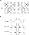
- the N denotes the number of the data units and is equal to 2 m , and the m is a positive integer. Taking 32 data units as an example, during a process of data unit replacement, a replacement operation of four data units, a replacement operation of eight data units, a replacement operation of 16 data units and a replacement operation of 32 data units is performed on the 32 data units successively according to the configured patterns.
- the patterns are: parameters corresponding to final positions obtained after position replacement of data units of an input vector processor. For example, assuming that four data units e0, e1, e2, and e3 are input from left to right, a position sequence to be output is e3, e0, e1, and e2, then the values of parameters p0, p1, p2, and p3 of patterns are configured as 1, 2, 3, and 0 respectively.
- the patterns further include cross selectors required for data exchanging, i.e., a configuration of control lines corresponding to 2-to-1 selectors.
- the disclosure is described by taking 32 data units as an example. However, the solution of the disclosure is not limited to arbitrary position replacement of 32 data units, but can also apply to arbitrary replacement of 64 or more data units. Of course, the disclosure supports arbitrary replacement of 4, 8 and 16 data units, and a specific implementation method of the disclosure is described below.
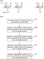
- Fig. 2 is a schematic flowchart of implementing a method of supporting arbitrary replacement of 32 data units according to an embodiment of the disclosure. As shown in Fig. 2 , an implementation flow of the method includes:
- a replacement operation is performed on the 32 data units of two groups on which the replacement operation of 16 data units has been performed in Step 204 to obtain a 32 data unit sequence according to the patterns, that is, the two groups of data units on which the replacement operation is performed in Step 204 are combined to generate one group of a 32 data unit sequence, and the replacement operation of 32 data units is performed according to the configured patterns.
- Fig. 8 is a flowchart of performing position replacement of 32 data units according to an embodiment of the disclosure.
- an replacement is performed on data units d0, d1, d2, ... , and d31.
- the 32 data units are denoted by d0 to d31 so as to distinguish 32 data units on which position replacement of 16 data units is performed in Step 204, and a result after performing the replacement operation of 16 data units on 32 data units c0, c1, c2, ..., and c31 is denoted by d0, d1, d2, ..., and d31.
- a time delay of the 2-to-1 selector is about 0.2 ns. If the 2-to-1 selector needs to operate at 500 MHz, then an arbitrary replacement operation of 32 data units needs to take two clock cycles, and is very quick.
- a time delay in a TSMC low power consumption library of 65 ns is generally less than 0.2 ns.
- the disclosure further discloses a device of supporting arbitrary replacement of multiple data units, which includes a configuring module and a replacement processing module.
- the configuring module is configured to configure patterns for arbitrary position replacement of N data units; and the replacement processing module is configured to, during a process of data unit replacement, perform a replacement operation on the N data units according to the patterns configured by the configuring module.
- the configuring module is configured to configure patterns for arbitrary position replacement of 32 data units; and the replacement processing module is configured to, during a process of data unit replacement, perform the following replacement operations successively on the 32 data units according to the patterns configured by the configuring module: a replacement operation of four data units, a replacement operation of eight data units, a replacement operation of 16 data units, and a replacement operation of 32 data units on the 32 data units.
- the configuring module can either be implemented by software or be implemented by hardware.
- the configuring module is preferably implemented by software, which can decrease an occupied area of the device in a chip.
- the replacement processing module includes a four data unit replacement module, an eight data unit replacement module, a 16 data unit replacement module, and a 32 data unit replacement module.
- the four data unit replacement module is configured to perform the replacement operation of four data units on the 32 data units according to the patterns configured by the configuring module, and send a replacement result to the eight data unit replacement module;
- the eight data unit replacement module is configured to perform the replacement operation of eight data units on 32 data units sent by the four data unit replacement module according to the patterns configured by the configuring module, and send a replacement result to the 16 data unit replacement module;
- the 16 data unit replacement module is configured to perform the replacement operation of 16 data units on 32 data units sent by the eight data unit replacement module according to the patterns configured by the configuring module, and send a replacement result to the 32 data unit replacement module;
- the 32 data unit replacement module is configured to perform the replacement operation of 32 data units on 32 data units sent by the 16 data unit replacement module according to the patterns configured by the configuring module.
- the solution of the disclosure can be extensively used to arbitrary position replacement of vector data units in a vector processor or arbitrary position replacement of parallel multiple data units in other applications.
Landscapes
- Engineering & Computer Science (AREA)
- Computer Hardware Design (AREA)
- Theoretical Computer Science (AREA)
- General Engineering & Computer Science (AREA)
- Computer Networks & Wireless Communication (AREA)
- Signal Processing (AREA)
- Physics & Mathematics (AREA)
- General Physics & Mathematics (AREA)
- Computing Systems (AREA)
- Microelectronics & Electronic Packaging (AREA)
- Design And Manufacture Of Integrated Circuits (AREA)
- Logic Circuits (AREA)
Claims (8)
- Procédé de prise en charge de remplacement arbitraire de multiples unités de données dans un processeur vectoriel, comprenant la configuration de schémas pour le remplacement arbitraire de position de 32 unités de données, caractérisé en ce que le procédé comprend :au cours d'un processus de remplacement d'unités de données, la réalisation d'une opération de remplacement sur les 32 unités de données conformément aux schémas configurés,la configuration (S201) de schémas pour le remplacement arbitraire de position de 32 unités de données, etau cours d'un processus de remplacement d'unités de données, la réalisation (S202, S203, S204, S205) des opérations de remplacement suivantes, successivement, sur les 32 unités de données conformément aux schémas configurés : une opération de remplacement de quatre unités de données, une opération de remplacement de huit unités de données, une opération de remplacement de 16 unités de données, et une opération de remplacement de 32 unités de données ;en sachant que : des opérations d'échange de trois ordres sont réalisées lors de la réalisation de l'opération de remplacement de quatre unités de données ; des opérations d'échange de trois ordres sont réalisées lors de la réalisation de l'opération de remplacement de huit unités de données ; des opérations d'échange de quatre ordres sont réalisées lors de la réalisation de l'opération de remplacement de 16 unités de données ; et des opérations d'échange de cinq ordres sont réalisées lors de la réalisation de l'opération de remplacement de 32 unités de données ; en réalisant ainsi des opérations d'échange de 3+3+4+5=15 ordres au cours du processus de remplacement d'unités de données.
- Procédé selon la revendication 1, dans lequel les schémas configurés comprennent :
une configuration de lignes de commande correspondant à des sélecteurs croisés, laquelle permet de commander une opération de remplacement de deux unités de données au cours d'un processus de remplacement. - Procédé selon la revendication 1, dans lequel l'étape de réalisation d'une opération de remplacement de quatre unités de données sur les 32 unités de données comprend :la division des 32 unités de données en huit groupes, chaque groupe comprenant quatre unités de données, etla réalisation d'une opération de remplacement sur les quatre unités de données du groupe respectif, respectivement.
- Procédé selon la revendication 1, dans lequel l'étape de réalisation d'une opération de remplacement de huit unités de données sur les 32 unités de données comprend :la réalisation d'une combinaison par paires sur quatre groupes d'unités de données sur lesquels l'opération de remplacement de huit unités de données est réalisée, pour produire quatre groupes de séquences de huit unités de données, etla réalisation de l'opération de remplacement de huit unités de données sur les quatre groupes de séquences d'unités de données, respectivement, conformément aux schémas configurés.
- Procédé selon la revendication 1, dans lequel l'étape de réalisation d'une opération de remplacement de 16 unités de données sur les 32 unités de données comprend :la réalisation d'une combinaison par paires sur quatre groupes d'unités de données sur lesquels l'opération de remplacement de huit unités de données est réalisée, pour produire deux groupes de séquences de 16 unités de données, etla réalisation de l'opération de remplacement de 16 unités de données sur les deux groupes de séquences d'unités de données, respectivement, conformément aux schémas configurés.
- Procédé selon la revendication 1, dans lequel l'étape de réalisation d'une opération de remplacement de 32 unités de données sur les 32 unités de données comprend :la combinaison de deux groupes d'unités de données sur lesquels l'opération de remplacement de 16 unités de données est réalisée, pour produire un groupe d'une séquence de 32 unités de données, etla réalisation de l'opération de remplacement de 32 unités de données sur le groupe de séquence d'unité de données conformément aux schémas configurés.
- Dispositif de prise en charge de remplacement arbitraire de multiples unités de données, caractérisé en ce qu'il comprend un module de configuration et un module de traitement de remplacement, et dans lequel
le module de configuration est conçu pour configurer des schémas pour le remplacement arbitraire de position de 32 unités de données, et
le module de traitement de remplacement est conçu pour, au cours d'un processus de remplacement d'unités de données, réaliser une opération de remplacement sur les 32 unités de données conformément aux schémas configurés par le module de configuration ;
le module de configuration est conçu pour configurer des schémas pour le remplacement arbitraire de position de 32 unités de données, et
le module de traitement de remplacement est conçu pour, au cours d'un processus de remplacement d'unités de données, réaliser les opérations de remplacement suivantes, successivement, sur les 32 unités de données conformément aux schémas configurés par le module de configuration : une opération de remplacement de quatre unités de données, une opération de remplacement de huit unités de données, une opération de remplacement de 16 unités de données, et une opération de remplacement de 32 unités de données ;
en sachant que : le module de traitement de remplacement est conçu en outre pour réaliser des opérations d'échange de trois ordres lors de la réalisation de l'opération de remplacement de quatre unités de données ; réaliser des opérations d'échange de trois ordres lors de la réalisation de l'opération de remplacement de huit unités de données ; réaliser des opérations d'échange de quatre ordres lors de la réalisation de l'opération de remplacement de 16 unités de données ; et réaliser des opérations d'échange de cinq ordres lors de la réalisation de l'opération de remplacement de 32 unités de données ; en réalisant ainsi des opérations d'échange de 3+3+4+5=15 ordres au cours du processus de remplacement d'unités de données. - Dispositif selon la revendication 7, dans lequel le module de traitement de remplacement comprend : un module de remplacement de quatre unités de données, un module de remplacement de huit unités de données, un module de remplacement de 16 unités de données, et un module de remplacement de 32 unités de données, et dans lequel
le module de remplacement de quatre unités de données est conçu pour réaliser l'opération de remplacement de quatre unités de données sur les 32 unités de données conformément aux schémas configurés par le module de configuration, et envoyer le résultat de remplacement au module de remplacement de huit unités de données,
le module de remplacement de huit unités de données est conçu pour réaliser l'opération de remplacement de huit unités de données sur 32 unités de données envoyées par le module de remplacement de quatre unités de données conformément aux schémas configurés par le module de configuration, et envoyer le résultat de remplacement au module de remplacement de 16 unités de données,
le module de remplacement de 16 unités de données est conçu pour réaliser l'opération de remplacement de 16 unités de données sur 32 unités de données envoyées par le module de remplacement de huit unités de données conformément aux schémas configurés par le module de configuration, et envoyer le résultat de remplacement au module de remplacement de 32 unités de données, et
le module de remplacement de 32 unités de données est conçu pour réaliser l'opération de remplacement de 32 unités de données sur 32 unités de données envoyées par le module de remplacement de 16 unités de données conformément aux schémas configurés par le module de configuration.
Applications Claiming Priority (2)
| Application Number | Priority Date | Filing Date | Title |
|---|---|---|---|
| CN201110086318.2A CN102737007B (zh) | 2011-04-07 | 2011-04-07 | 一种支持多个数据单元任意置换的方法和装置 |
| PCT/CN2011/082944 WO2012136065A1 (fr) | 2011-04-07 | 2011-11-25 | Procédé et dispositif de prise en charge de remplacement arbitraire parmi de multiples unités de données |
Publications (3)
| Publication Number | Publication Date |
|---|---|
| EP2696294A1 EP2696294A1 (fr) | 2014-02-12 |
| EP2696294A4 EP2696294A4 (fr) | 2017-03-01 |
| EP2696294B1 true EP2696294B1 (fr) | 2019-11-13 |
Family
ID=46968571
Family Applications (1)
| Application Number | Title | Priority Date | Filing Date |
|---|---|---|---|
| EP11863214.0A Not-in-force EP2696294B1 (fr) | 2011-04-07 | 2011-11-25 | Procédé et dispositif de prise en charge de remplacement arbitraire parmi de multiples unités de données |
Country Status (4)
| Country | Link |
|---|---|
| US (1) | US9332495B2 (fr) |
| EP (1) | EP2696294B1 (fr) |
| CN (1) | CN102737007B (fr) |
| WO (1) | WO2012136065A1 (fr) |
Families Citing this family (3)
| Publication number | Priority date | Publication date | Assignee | Title |
|---|---|---|---|---|
| CN109614365B (zh) * | 2018-11-14 | 2022-12-27 | 青岛海信日立空调系统有限公司 | Hbs芯片数据接收兼容电路 |
| CN109582635B (zh) * | 2018-11-14 | 2022-12-27 | 青岛海信日立空调系统有限公司 | Hbs芯片数据发送兼容电路 |
| CN110320957B (zh) * | 2019-08-05 | 2022-01-07 | 北京中科银河芯科技有限公司 | 一种电压选择电路 |
Family Cites Families (17)
| Publication number | Priority date | Publication date | Assignee | Title |
|---|---|---|---|---|
| US4078260A (en) * | 1976-05-12 | 1978-03-07 | International Business Machines Corporation | Apparatus for transposition sorting of equal length records in overlap relation with record loading and extraction |
| JP3344383B2 (ja) * | 1999-10-04 | 2002-11-11 | 日本電気株式会社 | スケジューラ |
| US6622242B1 (en) * | 2000-04-07 | 2003-09-16 | Sun Microsystems, Inc. | System and method for performing generalized operations in connection with bits units of a data word |
| CA2375058A1 (fr) * | 2000-05-05 | 2001-11-22 | Ruby B. Lee | Procede et systeme pour effectuer des permutations au moyen d'instructions de permutation basees sur un etage omega et un etage commute modifies |
| JP2003007065A (ja) * | 2001-06-21 | 2003-01-10 | Nec Microsystems Ltd | データ記憶回路、データ処理装置 |
| US7631025B2 (en) * | 2001-10-29 | 2009-12-08 | Intel Corporation | Method and apparatus for rearranging data between multiple registers |
| US6990552B2 (en) * | 2002-10-31 | 2006-01-24 | Mosaid Technologies, Inc. | Sorting method and apparatus using a CAM |
| DE112004000026D2 (de) * | 2003-04-04 | 2006-06-14 | Pact Xpp Technologies Ag | Verfahren und Vorrichtung für die Datenverarbeitung |
| CN100353702C (zh) * | 2004-01-20 | 2007-12-05 | 海信集团有限公司 | 可重构密码协处理器的可重构置换模块 |
| EP1769391A1 (fr) * | 2004-07-08 | 2007-04-04 | Asocs Ltd. | Procede et appareil pour la mise en oeuvre de transformees orthogonales rapides de taille variable |
| US7496590B2 (en) | 2005-07-26 | 2009-02-24 | Invensys Systems, Inc. | System and method for applying deadband filtering to time series data streams to be stored within an industrial process manufacturing/production database |
| JP4911223B2 (ja) * | 2007-06-06 | 2012-04-04 | 富士通株式会社 | 中継装置および端末装置 |
| US20090106525A1 (en) * | 2007-10-23 | 2009-04-23 | David Arnold Luick | Design structure for scalar precision float implementation on the "w" lane of vector unit |
| US8151031B2 (en) * | 2007-10-31 | 2012-04-03 | Texas Instruments Incorporated | Local memories with permutation functionality for digital signal processors |
| US8140932B2 (en) * | 2007-11-26 | 2012-03-20 | Motorola Mobility, Inc. | Data interleaving circuit and method for vectorized turbo decoder |
| CN101453292B (zh) * | 2007-11-30 | 2011-09-28 | 大唐移动通信设备有限公司 | 信道交织方法及装置 |
| JP2011023975A (ja) * | 2009-07-15 | 2011-02-03 | Seiko Epson Corp | データ転送装置、データ転送プログラム、データ転送システム、画像表示システム及びデータ転送方法 |
-
2011
- 2011-04-07 CN CN201110086318.2A patent/CN102737007B/zh not_active Expired - Fee Related
- 2011-11-25 US US14/008,562 patent/US9332495B2/en not_active Expired - Fee Related
- 2011-11-25 EP EP11863214.0A patent/EP2696294B1/fr not_active Not-in-force
- 2011-11-25 WO PCT/CN2011/082944 patent/WO2012136065A1/fr not_active Ceased
Non-Patent Citations (1)
| Title |
|---|
| None * |
Also Published As
| Publication number | Publication date |
|---|---|
| WO2012136065A1 (fr) | 2012-10-11 |
| EP2696294A4 (fr) | 2017-03-01 |
| EP2696294A1 (fr) | 2014-02-12 |
| US9332495B2 (en) | 2016-05-03 |
| CN102737007A (zh) | 2012-10-17 |
| US20140022971A1 (en) | 2014-01-23 |
| CN102737007B (zh) | 2015-01-28 |
Similar Documents
| Publication | Publication Date | Title |
|---|---|---|
| Lin et al. | Wireless network cloud: Architecture and system requirements | |
| JP7706569B2 (ja) | 端末能力レポート方法、ユーザ端末、及び通信システム | |
| US20080242347A1 (en) | Fast multiradio context switching | |
| US8989242B2 (en) | Encoding/decoding processor and wireless communication apparatus | |
| EP2696294B1 (fr) | Procédé et dispositif de prise en charge de remplacement arbitraire parmi de multiples unités de données | |
| US11206045B1 (en) | Efficient determination of parity bit location for polar codes | |
| WO2023009337A1 (fr) | Systèmes et procédés de partage de liaison ethernet pour simultanément prendre en charge de multiples radios | |
| CN115801016A (zh) | 可编程的数模转换器解码器系统和方法 | |
| EP3843272A1 (fr) | Convertisseur numérique-analogique, émetteur, station de base et dispositif mobile | |
| US8346182B2 (en) | Method and a device for dynamic reconfiguration of a radio communications system | |
| JP2011503913A (ja) | 異なる通信標準間のハンドオフのシステムおよび方法 | |
| Cabal et al. | High-speed computation of crc codes for fpgas | |
| US9824044B2 (en) | Common public radio interface (CPRI) lane controller coupled to direct memory access (DMA) wherein a time division duplex (TDD) steers control of CPRI | |
| US20040025004A1 (en) | Reconfigurable logic signal processor (RLSP) and method of configuring same | |
| US10075778B2 (en) | Base station with baseband bypass | |
| CN113452381B (zh) | 基于fpga的crc实现系统 | |
| CN119402914B (zh) | 基站前传接口封装处理器及报文封装方法 | |
| Sánchez-Ortiz et al. | Design and implementation of a multi-standard interleaver for 802.11 a, 802.11 n, 802.16 e & dvb standards | |
| EP3235335B1 (fr) | Appareil et procédé de commutation d'interface radio (ri) | |
| Zhai et al. | General Galois processor for transmitters in 5G/6G base stations | |
| US20090198973A1 (en) | Processing circuit | |
| JP4410842B2 (ja) | 演算装置 | |
| CN100596136C (zh) | 一种数据通道分组选择方法及装置 | |
| CN107547149B (zh) | 射频测试芯片 | |
| US20120293199A1 (en) | Programmable Priority Encoder |
Legal Events
| Date | Code | Title | Description |
|---|---|---|---|
| PUAI | Public reference made under article 153(3) epc to a published international application that has entered the european phase |
Free format text: ORIGINAL CODE: 0009012 |
|
| 17P | Request for examination filed |
Effective date: 20131010 |
|
| AK | Designated contracting states |
Kind code of ref document: A1 Designated state(s): AL AT BE BG CH CY CZ DE DK EE ES FI FR GB GR HR HU IE IS IT LI LT LU LV MC MK MT NL NO PL PT RO RS SE SI SK SM TR |
|
| DAX | Request for extension of the european patent (deleted) | ||
| RAP1 | Party data changed (applicant data changed or rights of an application transferred) |
Owner name: ZTE MICROELECTRONICS TECHNOLOGY CO., LTD |
|
| RA4 | Supplementary search report drawn up and despatched (corrected) |
Effective date: 20170131 |
|
| RIC1 | Information provided on ipc code assigned before grant |
Ipc: G06F 7/76 20060101ALI20170125BHEP Ipc: G06F 15/78 20060101AFI20170125BHEP |
|
| RAP1 | Party data changed (applicant data changed or rights of an application transferred) |
Owner name: SANECHIPS TECHNOLOGY CO., LTD. |
|
| STAA | Information on the status of an ep patent application or granted ep patent |
Free format text: STATUS: EXAMINATION IS IN PROGRESS |
|
| 17Q | First examination report despatched |
Effective date: 20190220 |
|
| GRAP | Despatch of communication of intention to grant a patent |
Free format text: ORIGINAL CODE: EPIDOSNIGR1 |
|
| STAA | Information on the status of an ep patent application or granted ep patent |
Free format text: STATUS: GRANT OF PATENT IS INTENDED |
|
| INTG | Intention to grant announced |
Effective date: 20190612 |
|
| GRAS | Grant fee paid |
Free format text: ORIGINAL CODE: EPIDOSNIGR3 |
|
| GRAA | (expected) grant |
Free format text: ORIGINAL CODE: 0009210 |
|
| STAA | Information on the status of an ep patent application or granted ep patent |
Free format text: STATUS: THE PATENT HAS BEEN GRANTED |
|
| AK | Designated contracting states |
Kind code of ref document: B1 Designated state(s): AL AT BE BG CH CY CZ DE DK EE ES FI FR GB GR HR HU IE IS IT LI LT LU LV MC MK MT NL NO PL PT RO RS SE SI SK SM TR |
|
| REG | Reference to a national code |
Ref country code: CH Ref legal event code: EP Ref country code: AT Ref legal event code: REF Ref document number: 1202401 Country of ref document: AT Kind code of ref document: T Effective date: 20191115 |
|
| REG | Reference to a national code |
Ref country code: DE Ref legal event code: R096 Ref document number: 602011063419 Country of ref document: DE |
|
| REG | Reference to a national code |
Ref country code: IE Ref legal event code: FG4D |
|
| REG | Reference to a national code |
Ref country code: CH Ref legal event code: NV Representative=s name: MURGITROYD AND COMPANY, CH |
|
| REG | Reference to a national code |
Ref country code: NL Ref legal event code: MP Effective date: 20191113 |
|
| REG | Reference to a national code |
Ref country code: LT Ref legal event code: MG4D |
|
| PG25 | Lapsed in a contracting state [announced via postgrant information from national office to epo] |
Ref country code: ES Free format text: LAPSE BECAUSE OF FAILURE TO SUBMIT A TRANSLATION OF THE DESCRIPTION OR TO PAY THE FEE WITHIN THE PRESCRIBED TIME-LIMIT Effective date: 20191113 Ref country code: LV Free format text: LAPSE BECAUSE OF FAILURE TO SUBMIT A TRANSLATION OF THE DESCRIPTION OR TO PAY THE FEE WITHIN THE PRESCRIBED TIME-LIMIT Effective date: 20191113 Ref country code: SE Free format text: LAPSE BECAUSE OF FAILURE TO SUBMIT A TRANSLATION OF THE DESCRIPTION OR TO PAY THE FEE WITHIN THE PRESCRIBED TIME-LIMIT Effective date: 20191113 Ref country code: NL Free format text: LAPSE BECAUSE OF FAILURE TO SUBMIT A TRANSLATION OF THE DESCRIPTION OR TO PAY THE FEE WITHIN THE PRESCRIBED TIME-LIMIT Effective date: 20191113 Ref country code: LT Free format text: LAPSE BECAUSE OF FAILURE TO SUBMIT A TRANSLATION OF THE DESCRIPTION OR TO PAY THE FEE WITHIN THE PRESCRIBED TIME-LIMIT Effective date: 20191113 Ref country code: NO Free format text: LAPSE BECAUSE OF FAILURE TO SUBMIT A TRANSLATION OF THE DESCRIPTION OR TO PAY THE FEE WITHIN THE PRESCRIBED TIME-LIMIT Effective date: 20200213 Ref country code: PT Free format text: LAPSE BECAUSE OF FAILURE TO SUBMIT A TRANSLATION OF THE DESCRIPTION OR TO PAY THE FEE WITHIN THE PRESCRIBED TIME-LIMIT Effective date: 20200313 Ref country code: GR Free format text: LAPSE BECAUSE OF FAILURE TO SUBMIT A TRANSLATION OF THE DESCRIPTION OR TO PAY THE FEE WITHIN THE PRESCRIBED TIME-LIMIT Effective date: 20200214 Ref country code: PL Free format text: LAPSE BECAUSE OF FAILURE TO SUBMIT A TRANSLATION OF THE DESCRIPTION OR TO PAY THE FEE WITHIN THE PRESCRIBED TIME-LIMIT Effective date: 20191113 Ref country code: FI Free format text: LAPSE BECAUSE OF FAILURE TO SUBMIT A TRANSLATION OF THE DESCRIPTION OR TO PAY THE FEE WITHIN THE PRESCRIBED TIME-LIMIT Effective date: 20191113 Ref country code: BG Free format text: LAPSE BECAUSE OF FAILURE TO SUBMIT A TRANSLATION OF THE DESCRIPTION OR TO PAY THE FEE WITHIN THE PRESCRIBED TIME-LIMIT Effective date: 20200213 |
|
| PG25 | Lapsed in a contracting state [announced via postgrant information from national office to epo] |
Ref country code: HR Free format text: LAPSE BECAUSE OF FAILURE TO SUBMIT A TRANSLATION OF THE DESCRIPTION OR TO PAY THE FEE WITHIN THE PRESCRIBED TIME-LIMIT Effective date: 20191113 Ref country code: RS Free format text: LAPSE BECAUSE OF FAILURE TO SUBMIT A TRANSLATION OF THE DESCRIPTION OR TO PAY THE FEE WITHIN THE PRESCRIBED TIME-LIMIT Effective date: 20191113 Ref country code: IS Free format text: LAPSE BECAUSE OF FAILURE TO SUBMIT A TRANSLATION OF THE DESCRIPTION OR TO PAY THE FEE WITHIN THE PRESCRIBED TIME-LIMIT Effective date: 20200313 |
|
| REG | Reference to a national code |
Ref country code: DE Ref legal event code: R119 Ref document number: 602011063419 Country of ref document: DE |
|
| PG25 | Lapsed in a contracting state [announced via postgrant information from national office to epo] |
Ref country code: AL Free format text: LAPSE BECAUSE OF FAILURE TO SUBMIT A TRANSLATION OF THE DESCRIPTION OR TO PAY THE FEE WITHIN THE PRESCRIBED TIME-LIMIT Effective date: 20191113 |
|
| REG | Reference to a national code |
Ref country code: CH Ref legal event code: PL |
|
| PG25 | Lapsed in a contracting state [announced via postgrant information from national office to epo] |
Ref country code: RO Free format text: LAPSE BECAUSE OF FAILURE TO SUBMIT A TRANSLATION OF THE DESCRIPTION OR TO PAY THE FEE WITHIN THE PRESCRIBED TIME-LIMIT Effective date: 20191113 Ref country code: EE Free format text: LAPSE BECAUSE OF FAILURE TO SUBMIT A TRANSLATION OF THE DESCRIPTION OR TO PAY THE FEE WITHIN THE PRESCRIBED TIME-LIMIT Effective date: 20191113 Ref country code: LI Free format text: LAPSE BECAUSE OF NON-PAYMENT OF DUE FEES Effective date: 20191130 Ref country code: DK Free format text: LAPSE BECAUSE OF FAILURE TO SUBMIT A TRANSLATION OF THE DESCRIPTION OR TO PAY THE FEE WITHIN THE PRESCRIBED TIME-LIMIT Effective date: 20191113 Ref country code: CH Free format text: LAPSE BECAUSE OF NON-PAYMENT OF DUE FEES Effective date: 20191130 Ref country code: LU Free format text: LAPSE BECAUSE OF NON-PAYMENT OF DUE FEES Effective date: 20191125 Ref country code: CZ Free format text: LAPSE BECAUSE OF FAILURE TO SUBMIT A TRANSLATION OF THE DESCRIPTION OR TO PAY THE FEE WITHIN THE PRESCRIBED TIME-LIMIT Effective date: 20191113 |
|
| REG | Reference to a national code |
Ref country code: AT Ref legal event code: MK05 Ref document number: 1202401 Country of ref document: AT Kind code of ref document: T Effective date: 20191113 |
|
| REG | Reference to a national code |
Ref country code: BE Ref legal event code: MM Effective date: 20191130 |
|
| PG25 | Lapsed in a contracting state [announced via postgrant information from national office to epo] |
Ref country code: SM Free format text: LAPSE BECAUSE OF FAILURE TO SUBMIT A TRANSLATION OF THE DESCRIPTION OR TO PAY THE FEE WITHIN THE PRESCRIBED TIME-LIMIT Effective date: 20191113 Ref country code: SK Free format text: LAPSE BECAUSE OF FAILURE TO SUBMIT A TRANSLATION OF THE DESCRIPTION OR TO PAY THE FEE WITHIN THE PRESCRIBED TIME-LIMIT Effective date: 20191113 Ref country code: MC Free format text: LAPSE BECAUSE OF FAILURE TO SUBMIT A TRANSLATION OF THE DESCRIPTION OR TO PAY THE FEE WITHIN THE PRESCRIBED TIME-LIMIT Effective date: 20191113 |
|
| PLBE | No opposition filed within time limit |
Free format text: ORIGINAL CODE: 0009261 |
|
| STAA | Information on the status of an ep patent application or granted ep patent |
Free format text: STATUS: NO OPPOSITION FILED WITHIN TIME LIMIT |
|
| 26N | No opposition filed |
Effective date: 20200814 |
|
| GBPC | Gb: european patent ceased through non-payment of renewal fee |
Effective date: 20200213 |
|
| PG25 | Lapsed in a contracting state [announced via postgrant information from national office to epo] |
Ref country code: IE Free format text: LAPSE BECAUSE OF NON-PAYMENT OF DUE FEES Effective date: 20191125 Ref country code: DE Free format text: LAPSE BECAUSE OF NON-PAYMENT OF DUE FEES Effective date: 20200603 Ref country code: FR Free format text: LAPSE BECAUSE OF NON-PAYMENT OF DUE FEES Effective date: 20200113 |
|
| PG25 | Lapsed in a contracting state [announced via postgrant information from national office to epo] |
Ref country code: SI Free format text: LAPSE BECAUSE OF FAILURE TO SUBMIT A TRANSLATION OF THE DESCRIPTION OR TO PAY THE FEE WITHIN THE PRESCRIBED TIME-LIMIT Effective date: 20191113 Ref country code: BE Free format text: LAPSE BECAUSE OF NON-PAYMENT OF DUE FEES Effective date: 20191130 Ref country code: AT Free format text: LAPSE BECAUSE OF FAILURE TO SUBMIT A TRANSLATION OF THE DESCRIPTION OR TO PAY THE FEE WITHIN THE PRESCRIBED TIME-LIMIT Effective date: 20191113 |
|
| PG25 | Lapsed in a contracting state [announced via postgrant information from national office to epo] |
Ref country code: IT Free format text: LAPSE BECAUSE OF FAILURE TO SUBMIT A TRANSLATION OF THE DESCRIPTION OR TO PAY THE FEE WITHIN THE PRESCRIBED TIME-LIMIT Effective date: 20191113 Ref country code: GB Free format text: LAPSE BECAUSE OF NON-PAYMENT OF DUE FEES Effective date: 20200213 |
|
| PG25 | Lapsed in a contracting state [announced via postgrant information from national office to epo] |
Ref country code: CY Free format text: LAPSE BECAUSE OF FAILURE TO SUBMIT A TRANSLATION OF THE DESCRIPTION OR TO PAY THE FEE WITHIN THE PRESCRIBED TIME-LIMIT Effective date: 20191113 |
|
| PG25 | Lapsed in a contracting state [announced via postgrant information from national office to epo] |
Ref country code: MT Free format text: LAPSE BECAUSE OF FAILURE TO SUBMIT A TRANSLATION OF THE DESCRIPTION OR TO PAY THE FEE WITHIN THE PRESCRIBED TIME-LIMIT Effective date: 20191113 Ref country code: HU Free format text: LAPSE BECAUSE OF FAILURE TO SUBMIT A TRANSLATION OF THE DESCRIPTION OR TO PAY THE FEE WITHIN THE PRESCRIBED TIME-LIMIT; INVALID AB INITIO Effective date: 20111125 |
|
| PG25 | Lapsed in a contracting state [announced via postgrant information from national office to epo] |
Ref country code: TR Free format text: LAPSE BECAUSE OF FAILURE TO SUBMIT A TRANSLATION OF THE DESCRIPTION OR TO PAY THE FEE WITHIN THE PRESCRIBED TIME-LIMIT Effective date: 20191113 |
|
| PG25 | Lapsed in a contracting state [announced via postgrant information from national office to epo] |
Ref country code: MK Free format text: LAPSE BECAUSE OF FAILURE TO SUBMIT A TRANSLATION OF THE DESCRIPTION OR TO PAY THE FEE WITHIN THE PRESCRIBED TIME-LIMIT Effective date: 20191113 |