EP2700984A1 - Film prismatique et procédé et appareil de fabrication de celui-ci - Google Patents
Film prismatique et procédé et appareil de fabrication de celui-ci Download PDFInfo
- Publication number
- EP2700984A1 EP2700984A1 EP13181248.9A EP13181248A EP2700984A1 EP 2700984 A1 EP2700984 A1 EP 2700984A1 EP 13181248 A EP13181248 A EP 13181248A EP 2700984 A1 EP2700984 A1 EP 2700984A1
- Authority
- EP
- European Patent Office
- Prior art keywords
- prism
- laser
- photoresist
- reflecting
- unit
- Prior art date
- Legal status (The legal status is an assumption and is not a legal conclusion. Google has not performed a legal analysis and makes no representation as to the accuracy of the status listed.)
- Ceased
Links
Images

Classifications
-
- G—PHYSICS
- G02—OPTICS
- G02B—OPTICAL ELEMENTS, SYSTEMS OR APPARATUS
- G02B5/00—Optical elements other than lenses
- G02B5/04—Prisms
- G02B5/045—Prism arrays
-
- G—PHYSICS
- G02—OPTICS
- G02B—OPTICAL ELEMENTS, SYSTEMS OR APPARATUS
- G02B3/00—Simple or compound lenses
- G02B3/0006—Arrays
- G02B3/0037—Arrays characterized by the distribution or form of lenses
- G02B3/0043—Inhomogeneous or irregular arrays, e.g. varying shape, size, height
-
- G—PHYSICS
- G03—PHOTOGRAPHY; CINEMATOGRAPHY; ANALOGOUS TECHNIQUES USING WAVES OTHER THAN OPTICAL WAVES; ELECTROGRAPHY; HOLOGRAPHY
- G03B—APPARATUS OR ARRANGEMENTS FOR TAKING PHOTOGRAPHS OR FOR PROJECTING OR VIEWING THEM; APPARATUS OR ARRANGEMENTS EMPLOYING ANALOGOUS TECHNIQUES USING WAVES OTHER THAN OPTICAL WAVES; ACCESSORIES THEREFOR
- G03B27/00—Photographic printing apparatus
- G03B27/72—Controlling or varying light intensity, spectral composition, or exposure time in photographic printing apparatus
-
- G—PHYSICS
- G03—PHOTOGRAPHY; CINEMATOGRAPHY; ANALOGOUS TECHNIQUES USING WAVES OTHER THAN OPTICAL WAVES; ELECTROGRAPHY; HOLOGRAPHY
- G03F—PHOTOMECHANICAL PRODUCTION OF TEXTURED OR PATTERNED SURFACES, e.g. FOR PRINTING, FOR PROCESSING OF SEMICONDUCTOR DEVICES; MATERIALS THEREFOR; ORIGINALS THEREFOR; APPARATUS SPECIALLY ADAPTED THEREFOR
- G03F7/00—Photomechanical, e.g. photolithographic, production of textured or patterned surfaces, e.g. printing surfaces; Materials therefor, e.g. comprising photoresists; Apparatus specially adapted therefor
- G03F7/0005—Production of optical devices or components in so far as characterised by the lithographic processes or materials used therefor
- G03F7/001—Phase modulating patterns, e.g. refractive index patterns
-
- G—PHYSICS
- G03—PHOTOGRAPHY; CINEMATOGRAPHY; ANALOGOUS TECHNIQUES USING WAVES OTHER THAN OPTICAL WAVES; ELECTROGRAPHY; HOLOGRAPHY
- G03F—PHOTOMECHANICAL PRODUCTION OF TEXTURED OR PATTERNED SURFACES, e.g. FOR PRINTING, FOR PROCESSING OF SEMICONDUCTOR DEVICES; MATERIALS THEREFOR; ORIGINALS THEREFOR; APPARATUS SPECIALLY ADAPTED THEREFOR
- G03F7/00—Photomechanical, e.g. photolithographic, production of textured or patterned surfaces, e.g. printing surfaces; Materials therefor, e.g. comprising photoresists; Apparatus specially adapted therefor
- G03F7/70—Microphotolithographic exposure; Apparatus therefor
- G03F7/70408—Interferometric lithography; Holographic lithography; Self-imaging lithography, e.g. utilizing the Talbot effect
Definitions
- Embodiments of the present invention relate to a prism film and a method and an apparatus for manufacturing the same.
- FIG. 1 illustrates a structure of a backlight in a LCD module.
- the backlight comprises a liquid crystal panel 1, a protective film 2, an upper prism film 3, a lower prism film 4, a diffusing film 5, a light guiding plate 6 and a bottom reflecting sheet 8 successively from top to bottom.
- the backlight further comprises a light source 9 located at least one side of the light guiding plate 6, a reflector 10 surrounding the light source 9 and open to the light guiding plate 6, and grids 7 disposed on the bottom surface of the light guiding plate 6.
- the protective film 2 may be unnecessary in some backlights.
- the structure of backlight can be in forms of any combination of the elements mentioned.
- the backlight is not limited to be applicable to a liquid crystal display device, but can be applicable to other display devices such as an electronic paper etc.
- the upper prism film 3 as shown in Figure 1 is mainly used for converging light.
- Fig.2 shows a conventional technology for fabricating the upper prism film; firstly a photoresist is formed on a surface of a substrate which may be composed of macromolecule polymers, for instance, the substrate may be composed of one layer or multi-layers of macromolecule polymers.
- the macromolecule polymers may be PET (polyethylene terephthalate) etc.
- the photoresist can be formed on the surface of the substrate by coating, sputtering or depositing, and then passing the substrate through a rotary wheel 13 with prism teeth.
- the shape defined by adjacent prism teeth on the rotary wheel 13 corresponds to the shape of the prism to be formed, and these prism teeth can form a prism structure on the photoresist.
- the photoresist is cured by a curing light source, such that the substrate and the structures of prism thereon constitute a prism film.
- the photoresist may be an UV photoresist
- the curing light source may be an UV curing light source accordingly. It can also adopt photoresists of other types as well as the corresponding curing light sources.
- the above technology for manufacturing prism film has the following disadvantages in practice: (1) the prism teeth of the rotary wheel are worn and deformed in use, so as to degrade the prism film; (2) when repairing the prism teeth or changing of the prism's parameters such as prism period, modulation depth etc., it needs to process the prism teeth with a machining method such as a laser processing method or a mechanical processing method.
- a machining method such as a laser processing method or a mechanical processing method.
- these processing methods are very complicated, as well as being high-cost and low time-efficient; (3) the modulation depth of the prism structure on the surface of prism film processed by the conventional technology is generally fixed, thereby it can not effectively avoid conglutination between the prism film and other films or the liquid crystal panel.
- embodiments of the present invention provide a prism film and a method and an apparatus for manufacturing the prism film, thereby obtaining a prism film with different modulation depths.
- Prism protrusion means a protrusion formed by the photoresist and defining the prism structure on the surface of the substrate;
- Prism period means a distance between two adjacent prism protrusions, it may be a distance between either the adjacent highest points or the lowest points of prism protrusions, but in this description it means a distance between the adjacent highest points of prism protrusions;
- Modulation depth means a protruding height of prism, and in this description it means a distance between a protruding highest point of prism and the substrate;
- Prism direction means a direction along which the prism protrusion extends on the substrate.
- the embodiments of present invention provide a prism film comprising a substrate, and a plurality of prism protrusions of photoresist disposed on the substrate; and modulation depths of at least two prism protrusions are different.
- the prism protrusions on the prism film provided by the embodiments of present invention are formed by interfering photoresist with laser beams; wherein the prism period is determined by the interference angle between the laser beams incident on the photoresist and the wavelength of the laser beam.
- the modulation depth is determined by the time of exposing the photoresist by laser and/or the time of developing the photoresist.
- a method for manufacturing a prism film comprises: coating a photoresist on a surface of a substrate; performing laser interference lithography on the photoresist; developing and fixing the photoresist processed by the laser interference lithography, and forming prism protrusions with different modulation depths on the surface of the substrate so as to obtain a fixed prism film; and performing dry-molding processing on the fixed prism film so as to obtain a final prism film.
- the laser interference lithography on the photoresist comprises the following steps: pre-heating and placing the substrate coated with the photoresist on a lithography platform; outputting a UV laser beam by a solid laser, expanding, collimating and splitting the UV laser beam to obtain two UV laser beams, and then expanding the two UV laser beams once again and converging them on a surface of the substrate coated with the photoresist at an interference angle ⁇ for the interference lithography.
- the above method further comprises the following steps: rotating the substrate coated with the photoresist in a plane perpendicular to the UV laser beams, and forming prism protrusions with different prism directions on the surface of the substrate; adjusting the prism period by changing the interference angle ⁇ and/or the wavelength of the laser beams.
- the embodiments of present invention also provide an interference lithography apparatus for manufacturing a prism film.
- the interference lithography apparatus comprises a solid laser, as well as a beam expanding unit, a collimating unit, a light splitting unit and a light converging unit; wherein, the beam expanding unit is used for expanding UV laser emitted from the solid laser, the collimating unit is used for collimating the expanded UV laser so as to obtain the collimated UV laser; the light splitting unit is used for splitting the collimated UV laser so as to obtain two collimated UV laser beams with a constant phase difference; the light converging unit is used for, on the surface of the substrate coated with the photoresist, converging the two collimated UV laser beams obtained by the splitting unit for the interference lithography.
- the beam expanding unit may be a beam expanding convex lens
- the collimating unit may be a collimating convex lens
- the focus of the beam expanding convex lens coincides with the focus of the collimating convex lens.
- the interference lithography apparatus also comprises: a reflecting unit for reflecting the collimated UV laser obtained by the collimating unit to the light splitting unit.
- the reflecting unit is a silver-plated reflector
- an included angle in a range of 10° to 170° is formed between a center axis direction of the reflecting unit and an incident direction of the collimated UV laser beam emitted from the collimating unit; the center axis direction of the reflecting unit means a normal direction perpendicular to the reflecting surface of the reflecting unit.
- An included angle of 45° is formed between the center axis direction of the reflecting unit and an incident direction of the collimated UV laser emitted from the collimating unit.
- the light converging unit comprises a first reflecting subunit, a second reflecting subunit, a first beam expanding subunit and a second beam expanding subunit.
- the light splitting unit is used for reflecting one half of the collimated UV laser beam to the first reflecting subunit, and transmitting the remaining half of the collimated UV laser beam to the second reflecting subunit.
- the first reflecting subunit is used for reflecting the incident collimated UV laser to the first beam expanding subunit;
- the second reflecting subunit is used for reflecting the incident collimated UV laser beam to the second beam expanding subunit;
- the first and second beam expanding subunits are used for expanding the incident collimated UV laser beams, and then converging the expanded UV laser beams on the surface of the substrate coated with the photoresist at an interference angle ⁇ for the interference lithography.
- the first and second reflecting subunits are reflectors
- the first and second reflecting subunits are arranged symmetrically by taking the reflecting surface of the light splitting unit as a symmetry plane.
- the positions of the first and second beam expanding subunits are determined on the basis of focal lengths thereof and sizes of the interference light spots formed on the surface of the substrate coated with the photoresist.
- the interference lithography apparatus further comprises a lithography platform, which can rotate in a plane perpendicular to an incident direction of laser beams, and move parallelly with respect to the light converging unit.
- the substrate coated with the photoresist can rotate in a plane perpendicular to the UV laser by means of rotation of the lithography platform, and the prism protrusions with different prism directions are finally formed on the surface of the substrate after the exposing, developing and fixing steps.
- the sizes of the interference light spots on the surface of the substrate coated with the photoresist can be adjusted through the moving of the lithography platform with respect to the light converging unit.
- the first and second reflecting subunits can move with respect to the reflecting surface of the light splitting unit, so as to adjust the sizes of interference light spots.
- the first and second reflecting subunits can rotate with respect to the reflecting surface of the light splitting unit, so as to adjust the interference angle between the laser beams.
- the first and second beam expanding subunits can move with respect to the first and second reflecting subunits, respectively, so as to adjust the sizes of interference light spots of the laser beams.
- the first and second beam expanding subunits can rotate with respect to the first and second reflecting subunits, respectively, so as to adjust the interference angle ⁇ .
- the embodiments of present invention manufacture a prism film by interference lithography with the advantages of high productivity and low cost. Since the modulation depth of prisms on the surface of the prism film is distributed randomly, it can effectively solve the problem of conglutination between the prism film and other films or liquid crystal panel. And moreover, since the direction and cycle of prism can be easily adjusted, it can effectively solve the problem of image display such as Morie fringe etc.
- Fig.1 illustrates a structural schematic diagram of the backlight in the liquid crystal display device
- Fig. 2 illustrates the process for manufacturing a prism film
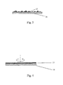
- Fig.3 illustrates a structural schematic diagram of the prism film according to one embodiment of the present invention
- Fig.4 illustrates a schematic diagram of coating a substrate with photoresist in one embodiment of the present invention
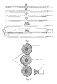
- Fig.5 illustrates a schematic diagram of Morie fringe formed by unmatched prism directions of the upper and lower prism films
- Figs.6a and 6b are schematic diagrams of the prism directions obtained before and after rotation of the substrate in one embodiment of the present invention.
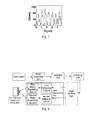
- Fig.7 is a graph showing the modulation depth of a prism film made by the method in accordance with one embodiment of the present invention and observed under an atomic force microscope;
- Fig.8 illustrates a structural schematic diagram of an interference lithography apparatus for the prism film in one embodiment of the present invention.
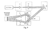
- Fig.9 illustrates a structural schematic diagram of an interference lithography apparatus for the prism film in one specific embodiment of the present invention.
- a method for manufacturing a prism film includes: coating a surface of a substrate with photoresist; performing the laser interference lithography on the photoresist; developing and fixing the photoresist processed by the laser interference lithography, forming prism protrusions with different modulation depths on the surface of the substrate, and obtaining a fixed prism film; performing dry-molding processing to the fixed prism film so as to obtain a final prism film.
- the prism film with modulation depth changed randomly can effectively prevent conglutination of films.
- Fig.3 shows that the prism film in accordance with one embodiment of the present invention comprises a substrate 16, and a plurality of prism protrusions 15 formed of photoresist on the substrate 16; at least two prism protrusions 15 have different heights.
- the prism protrusions 15 are formed by interference of laser beams on the photoresist; the prism period d is determined by the interference angle ⁇ between the incident laser beams on the photoresist for interference and/or the wavelength of the laser beam; the modulation depth M d of the prism protrusions 15 is determined by the time of exposing the photoresist to laser beams and/or the time of developing the photoresist. It is understood by those skilled in the art that the prism protrusions 15 may have various shapes, for instance, a spike protrusion or a circle protrusion etc.
- the method for manufacturing a prism film in accordance with one embodiment of the present invention shall be explained herein.
- the method comprises the steps as follows.
- the substrate is coated with photoresist.
- PET is used for making a substrate 16, and the substrate 16 is coated with the photoresist 17 such as photoresist SU8, and the substrate 16 is coated with the photoresist 17 uniformly by adjusting the rotating speed and the rotating time of a spin coater.
- the thickness of the photoresist can be adjusted by adjusting the rotating speed of the spin coater.
- the photoresist SU8 is a transparent epoxy resin; it has a small molecular weight and is a chain structure macromolecule before subject to irradiation of light; when subject to irradiation of UV rays, a polymerization occurs to SU8 and a latticed macromolecule is produced.
- the epoxy resin has a good chemical stability and high rigidity, and is a positive photoresist. It can be understood that the substrate can also be coated with other transparent photoresists with high optical transmissivity such as an UV photoresis etc.
- a laser interference lithography is performed on the photoresist.
- a pre-heated substrate coated with the photoresist is placed on a lithography platform; a UV laser beam is output by a solid laser, and then expanding, collimating and splitting the UV laser beam so as to obtain two UV laser beams, and subsequently, expanding the two UV laser beams once again, and converging them on the surface of the photoresist with an interference angle ⁇ for the interference lithography.
- the substrate coated with the photoresist can be rotated in a plane perpendicular to the UV laser, so as to form prism protrusions with different prism directions; thereby undesirable phenomenon, such as Morie fringe etc. produced in the process of developing film material of backlight, can be conveniently removed. It is noted over here that the produced Morie fringe is due to unmatched prism directions of the upper and lower prism films in the backlight, such that the fringes in periodical arrangement are formed in the display image.
- the undesirable Morie fringes can be removed through adjusting arranging angle of the prisms in the prism film, such that the prism directions of the upper and lower prism films are perpendicular to each other in theory, in this case, it can avoid the occurrence of Morie fringe in the display image.
- it needs to engrave the arranging directions of prism teeth on the rotary wheel once again so as to change the prism directions; that is, it is equivalent to make a new mould, thereby involving a long period of developing technology, a high cost and a complex procedures.
- the substrate is rotated by angle ⁇ on a plane perpendicular to a plane in which the interference laser beams are located, and then the prism direction produced by the laser interference changes with respect to the edge of the substrate.
- the prism direction is perpendicular to the bottom margin of the substrate; after rotating the substrate at angle ⁇ on a plane perpendicular to a plane on which the interference laser beams are located, the prism direction is perpendicular to the horizontal line, but having an included angel of 90- ⁇ degree with the bottom margin of the substrate (please refer to Fig.6b for the details).
- the substrate processed by the laser interference lithography is developed and fixed to form the prism protrusions with different modulation depths on the surface of photoresist on the substrate, and then a fixed prism film is obtained.
- the substrate coated with the photoresist processed by the laser interference lithography is developed and fixed, such that a plurality of microprism structures, i.e. a plurality of prism protrusions, with different modulation depths are formed on the surface of the substrate,.
- the prism protrusions may be spike protrusions or circle protrusions etc.
- the modulation depths on the surface of the prism film can be controlled by adjusting the time of the laser interference lithography for the photoresist on the substrate, i.e. adjusting the time of exposing the photoresist and/or the time of developing the photoresist. It can be understood that the modulation depths of the parims on the surface of the prism film can also be controlled by adjusting the intensity of the laser.
- the obtained modulation depth of the prism is 250 um; when exposing for 3 seconds and developing for seconds, the obtained modulation depth of the prism is 160 um.
- a better modulation depth can be obtained by optimizing the time parameters during developing a prism film. Prisms with different modulation depths can also be obtained by adopting the same exposing time and different developing times.
- the dry-molding processing is performed on the fixed prism film, so as to obtain a final prism film.
- other types of dry-shaping technology can be adopted.
- a heating technology can also be adopted for speeding up curing the photoresist and improving the rigidity of the photoresist.
- Fig.7 shows the modulation depth on the surface of the final prism film observed under an atomic force microscope (AFM), wherein the abscissa axis denotes a length direction of the prism film, i.e. a direction perpendicular to the direction of prism, and the ordinate axis denotes the modulation depth. As shown in Fig.7 , the modulation depth on the surface of the prism film is distributed randomly.
- AFM atomic force microscope
- the interference lithography apparatus comprises a solid laser, a beam expanding unit, a collimating unit, a light splitting unit and a light converging unit; wherein, the beam expanding unit is used for expanding a UV laser beam emitted from the solid laser, the collimating unit is used for collimating the expanded UV laser beam so as to obtain the collimated UV laser beam; the light splitting unit is used for splitting the collimated UV laser beam so as to obtain two collimated UV laser beams with a constant phase difference; the light converging unit is used for converging the two collimated UV laser beams obtained by the splitting unit on the surface of the substrate coated with the photoresist for the interference lithography.
- the beam expanding unit may be a beam expanding convex lens
- the collimating unit may be a collimating convex lens
- the focus of the beam expanding convex lens coincides with the focus of the collimating convex lens.
- the interference lithography apparatus also comprises a reflecting unit for reflecting the collimated UV laser obtained by the collimating unit to the light splitting unit.
- an included angle in a range of 10° to 170° is formed between a center axis direction of the reflecting unit and an incident direction of the collimated UV laser obtained by the collimating unit.
- an included angle of 45° is formed between the center axis direction of the reflecting unit and an incident direction of the collimated UV laser obtained by the collimating unit.
- the light converging unit may comprise a first reflecting subunit, a second reflecting subunit, a first beam expanding subunit and a second beam expanding subunit.
- the light splitting unit is used for reflecting one half of the collimated UV laser beam to the first reflecting subunit, and transmitting the remaining half of the collimated UV laser beam to the second reflecting subunit.
- the first reflecting subunit is used for reflecting the incident collimated UV laser beam to the first beam expanding subunit;
- the second reflecting subunit is used for reflecting the incident collimated UV laser beam to the second beam expanding subunit;
- the first and second beam expanding subunits are used for expanding the incident collimated UV laser beam, and then converging the expanded UV laser beams on the surface of the substrate coated with the photoresist at an interference angle ⁇ for the interference lithography.
- the first and second reflecting subunits are reflectors respectively
- the first and second reflecting subunits are arranged symmetrically by taking a reflecting surface of the light splitting unit as the symmetrical plane.
- the positions of the first and second beam expanding subunits are determined according to focal lengths thereof and sizes of the interference light spots formed on the surface of the substrate coated with the photoresist.
- Fig.9 illustrates the structural schematic diagram of an interference lithography apparatus for manufacturing a prism film in accordance with one specific embodiment of the present invention.
- the interference lithography apparatus comprises a solid laser, a beam expanding unit, a collimating unit, a reflecting unit, a light splitting unit and a light converging unit.
- the beam expanding unit is a convex lens L1
- the collimating unit is a convex lens L2
- the reflecting unit is a silver-plated reflector M1
- the light splitting unit is a transflective convex lens BS
- the first reflecting subunit is a reflector M2
- the first beam expanding subunit is a convex lens L3
- the second reflecting subunit is a reflector M3
- the second beam expanding subunit is a convex lens L4.
- the focus of the beam expanding unit L1 coincides with the focus of the collimating unit L2, and the focus of the beam expanding unit L1 is smaller than the focus of the collimating unit L2.
- all the optical devices are placed perpendicular to the surface of the tabletop.
- An included angle in a range of 10° to 170° is formed between the center axis direction of the reflecting unit M1 and the incident light direction.
- an included angle of 45° is formed between the center axis direction of the reflecting unit M1 and the incident light direction
- the whole interference lithography apparatus occupies a minimal area, wherein the distance between the reflecting unit M1 and the collimating unit L2 can be set flexibly according to the actual situation, for example, 5cm etc.
- the included angle between the light splitting unit and the incident light direction can be adjusted based on the interference angle ⁇ and the distance between the first and second reflecting subunits M2, M3 and the substrate coated with the photoresist.
- the first and second reflecting subunits M2 and M3 are arranged symmetrically by taking a reflecting surface of the light splitting unit as a symmetrical plane, so as to ensure the interference light beams irradiating the substrate coated with the photoresist symmetrically with respect to the reflecting surface of the light splitting unit.
- the positions of the beam expanding L1, the collimating unit L2, the first beam expanding subunit L3 and the second beam expanding subunit L4 can be adjusted according to the focal lengths of the selected convex lenses and the sizes of the interference light spots to be formed on the photoresist.
- the first reflecting subunit M2 and the second reflecting subunit M3 can move with respect to the reflecting surface of the light splitting unit in a manner of mirror image, that is to say, if the first reflecting subunit M2 get closer to the light splitting unit, the second reflecting subunit M3 also get closer to the light splitting unit, and vice versa, so as to adjust the sizes of interference light spots.
- the first reflecting subunit M2 and the second reflecting subunit M3 can rotate with respect to the each other's mirror image of the reflecting surface of the light splitting unit, so as to adjust the size of the interference angle ⁇ .
- the first beam expanding subunit L3 and the second beam expanding subunit L4 can move with respect to the first reflecting subunit M2 and the second reflecting subunit M3 respectively, so as to adjust the sizes of the interference light spots.
- the first beam expanding subunit L3 and the second beam expanding subunit L4 can rotate with respect to the first reflecting subunit M2 and the second reflecting subunit M3 respectively, so as to adjust the size of the interference angle ⁇ .
- the interference lithography apparatus further comprises a lithography platform, which can rotate, and can move with respect to the light converging unit.
- the prism direction can be adjusted by the rotation of the lithography platform; and the sizes of the interference light spots irradiated on the substrate coated with the photoresist can also be adjusted through the moving of the lithography platform with respect to the light converging unit.
- the solid laser emits an UV laser beam with a wavelength of 355nm
- the light splitting unit can be a transflective beam splitter which can split the UV laser beam with a wavelength of 355nm into two.
- the operating principle of the laser interference lithography apparatus is: Nd:YAG solid laser outputs an UV laser beam with a wavelength of 355nm; after the UV laser beam is expanded by the beam expanding unit L1, collimated by the collimating unit L2, and splitted by the light splitting unit BS, the two light beams obtained are converged by the light converging unit on the surface of the photoresist on the substrate for the interference lithography.
- the wavelength of the laser output by the solid laser is adjustable, the wavelength of the laser beam output by the solid laser can be adjusted according to the above formula in order to obtain the desired prism period d.
- the first beam expanding subunit L3 and the second beam expanding subunit L4 are used for expanding the light beams reflected by the first reflecting subunit M2 and the second reflecting subunit M3 respectively, so as to form larger interference light spots on the surface of the photoresist on the substrate to be processed, thereby reducing the length of light path.
- the light beams reflected by the first reflecting subunit M2 and the second reflecting subunit M3 are converged on the surface of the photoresist on the substrate at an included angle ⁇ , so as to form alternate dark and bright grating fringes, wherein the grating fringe of 0 grade at the central position of the long edge of the substrate coated with the photoresist has the strongest brightness, and the intensity of light is successively and symmetrically reduced towards both sides; after the developing and fixing, it may form prism protrusions, i.e. prism structure, with modulation depths distributed randomly on the surface of the substrate due to uneven coated photoresist and structural characteristics of the photoresist.
Landscapes
- Physics & Mathematics (AREA)
- General Physics & Mathematics (AREA)
- Optics & Photonics (AREA)
- Spectroscopy & Molecular Physics (AREA)
- Exposure And Positioning Against Photoresist Photosensitive Materials (AREA)
- Optical Elements Other Than Lenses (AREA)
- Exposure Of Semiconductors, Excluding Electron Or Ion Beam Exposure (AREA)
Applications Claiming Priority (1)
| Application Number | Priority Date | Filing Date | Title |
|---|---|---|---|
| CN201210301889.8A CN103630953B (zh) | 2012-08-22 | 2012-08-22 | 一种棱镜膜及其制备方法及装置 |
Publications (1)
| Publication Number | Publication Date |
|---|---|
| EP2700984A1 true EP2700984A1 (fr) | 2014-02-26 |
Family
ID=49036438
Family Applications (1)
| Application Number | Title | Priority Date | Filing Date |
|---|---|---|---|
| EP13181248.9A Ceased EP2700984A1 (fr) | 2012-08-22 | 2013-08-21 | Film prismatique et procédé et appareil de fabrication de celui-ci |
Country Status (3)
| Country | Link |
|---|---|
| US (1) | US9885811B2 (fr) |
| EP (1) | EP2700984A1 (fr) |
| CN (1) | CN103630953B (fr) |
Families Citing this family (10)
| Publication number | Priority date | Publication date | Assignee | Title |
|---|---|---|---|---|
| JP6699092B2 (ja) * | 2015-04-28 | 2020-05-27 | 大日本印刷株式会社 | 樹脂シートの製造方法 |
| CN105114833B (zh) * | 2015-07-22 | 2018-01-23 | 武汉华星光电技术有限公司 | 聚光led、背光模组及聚光led的制造方法 |
| CN105789485B (zh) * | 2016-03-14 | 2017-12-26 | 淮阴工学院 | 一种全息散斑结构有机发光二极管制作方法 |
| CN106646716A (zh) * | 2017-02-14 | 2017-05-10 | 山西大学 | 空间堆叠型光束分布式相位延迟器及其散斑消除方法 |
| CN110456558B (zh) * | 2018-05-08 | 2022-08-19 | 京东方科技集团股份有限公司 | 光学膜材、背光源及显示装置 |
| US11131929B2 (en) | 2018-11-07 | 2021-09-28 | Waymo Llc | Systems and methods that utilize angled photolithography for manufacturing light guide elements |
| US11131934B2 (en) | 2019-10-29 | 2021-09-28 | Waymo Llc | Non-telecentric light guide elements |
| CN112505811A (zh) * | 2020-10-10 | 2021-03-16 | 上海宏盾防伪材料有限公司 | 一种非对称光栅结构图案的制作方法 |
| KR102990349B1 (ko) * | 2020-12-16 | 2026-07-10 | 엘지디스플레이 주식회사 | 다각패턴 마이크로렌즈 어레이 및 이를 구비한 표시장치 |
| CN114879401B (zh) * | 2022-04-28 | 2023-10-31 | Tcl华星光电技术有限公司 | 显示模组 |
Citations (6)
| Publication number | Priority date | Publication date | Assignee | Title |
|---|---|---|---|---|
| US4013465A (en) * | 1973-05-10 | 1977-03-22 | Secretary Of State For Defence In Her Britannic Majesty's Government Of The United Kingdom Of Great Britain And Northern Ireland | Reducing the reflectance of surfaces to radiation |
| EP0271002A2 (fr) * | 1986-12-06 | 1988-06-15 | Kuraray Co., Ltd. | Photomasque de facteur de transmission modulé, procédé de sa fabrication et procédé de fabrication d'un réseau de diffraction |
| GB2349237A (en) * | 1999-04-24 | 2000-10-25 | Sharp Kk | An optical element, method of manufacture thereof and a display device incorporating said element. |
| US20040190102A1 (en) * | 2000-08-18 | 2004-09-30 | Mullen Patrick W. | Differentially-cured materials and process for forming same |
| EP1916551A1 (fr) * | 2006-10-26 | 2008-04-30 | K Laser Technology, Inc. | Matrice de prisme avec structures de phase aléatoires |
| US20110032727A1 (en) * | 2007-12-20 | 2011-02-10 | Kinder Brian A | Backlight reflectors having a prismatic structure |
Family Cites Families (12)
| Publication number | Priority date | Publication date | Assignee | Title |
|---|---|---|---|---|
| US6258443B1 (en) * | 1994-09-28 | 2001-07-10 | Reflexite Corporation | Textured retroreflective prism structures and molds for forming same |
| US7195872B2 (en) * | 2001-11-09 | 2007-03-27 | 3D Biosurfaces, Inc. | High surface area substrates for microarrays and methods to make same |
| JP2003240962A (ja) * | 2002-02-15 | 2003-08-27 | Sanyo Electric Co Ltd | 導光板およびこれを用いた面光源装置 |
| KR100432347B1 (ko) * | 2003-07-01 | 2004-05-20 | 주식회사 엘지에스 | 백라이트 유닛의 집광시트 |
| TW200600919A (en) * | 2004-06-22 | 2006-01-01 | Samsung Electronics Co Ltd | Optical film, backlight assembly and liquid crystal display device having the same |
| JP2008530346A (ja) * | 2005-02-17 | 2008-08-07 | スリーエム イノベイティブ プロパティズ カンパニー | 低ガラス転移温度を有する重合有機相を含む輝度向上フィルム |
| KR100935717B1 (ko) * | 2007-09-03 | 2010-01-08 | 제일모직주식회사 | 능선이 기울기를 가지도록 형성된 프리즘 시트 및 이를이용한 액정표시장치 |
| CN101566793A (zh) * | 2008-04-23 | 2009-10-28 | 中国科学院半导体研究所 | 用于制备二维光子晶体的双光束全息干涉多次曝光方法 |
| CN101295047A (zh) * | 2008-06-27 | 2008-10-29 | 长兴化学工业股份有限公司 | 光学膜 |
| CN201935118U (zh) * | 2010-12-29 | 2011-08-17 | 京东方科技集团股份有限公司 | 棱镜片、背光源及其液晶显示装置 |
| CN102141736A (zh) * | 2011-01-05 | 2011-08-03 | 中国科学院半导体研究所 | 紫外激光干涉条纹的辅助检测装置及方法 |
| TWI484307B (zh) * | 2012-10-29 | 2015-05-11 | Nat Univ Tsing Hua | 以光纖作為空間濾波器與擴束器之雷射干涉微影設備 |
-
2012
- 2012-08-22 CN CN201210301889.8A patent/CN103630953B/zh not_active Expired - Fee Related
-
2013
- 2013-08-21 US US13/972,142 patent/US9885811B2/en not_active Expired - Fee Related
- 2013-08-21 EP EP13181248.9A patent/EP2700984A1/fr not_active Ceased
Patent Citations (6)
| Publication number | Priority date | Publication date | Assignee | Title |
|---|---|---|---|---|
| US4013465A (en) * | 1973-05-10 | 1977-03-22 | Secretary Of State For Defence In Her Britannic Majesty's Government Of The United Kingdom Of Great Britain And Northern Ireland | Reducing the reflectance of surfaces to radiation |
| EP0271002A2 (fr) * | 1986-12-06 | 1988-06-15 | Kuraray Co., Ltd. | Photomasque de facteur de transmission modulé, procédé de sa fabrication et procédé de fabrication d'un réseau de diffraction |
| GB2349237A (en) * | 1999-04-24 | 2000-10-25 | Sharp Kk | An optical element, method of manufacture thereof and a display device incorporating said element. |
| US20040190102A1 (en) * | 2000-08-18 | 2004-09-30 | Mullen Patrick W. | Differentially-cured materials and process for forming same |
| EP1916551A1 (fr) * | 2006-10-26 | 2008-04-30 | K Laser Technology, Inc. | Matrice de prisme avec structures de phase aléatoires |
| US20110032727A1 (en) * | 2007-12-20 | 2011-02-10 | Kinder Brian A | Backlight reflectors having a prismatic structure |
Also Published As
| Publication number | Publication date |
|---|---|
| US9885811B2 (en) | 2018-02-06 |
| CN103630953A (zh) | 2014-03-12 |
| US20140055861A1 (en) | 2014-02-27 |
| CN103630953B (zh) | 2016-08-03 |
Similar Documents
| Publication | Publication Date | Title |
|---|---|---|
| US9885811B2 (en) | Prism film and method and apparatus for manufacturing the same | |
| US11378812B2 (en) | Diffuser plate and method for designing diffuser plate | |
| US20140126029A1 (en) | Method and device for the layered production of thin volume grid stacks, and beam combiner for a holographic display | |
| US20100020400A1 (en) | Diffractive optical element, method for manufacturing diffractive optical element, and laser beam machining method | |
| US8221963B2 (en) | Method for producing fine structure | |
| US20240337950A1 (en) | Apparatus and method for laser interference structuring of substrates with periodic dot structures for anti-reflection properties | |
| JP2010179496A (ja) | 光造形装置及び造形ベース | |
| JP2010079200A (ja) | 光学素子、反射防止機能付き光学部品、および原盤 | |
| JP2008525850A (ja) | 光学的基板及びその製造方法 | |
| KR20000057318A (ko) | 광 확산용 광학 구조물 | |
| US20120224263A1 (en) | Optical Systems Utilizing Diffraction Gratings To Remove Undesirable Light From A Field Of View | |
| WO2013183708A1 (fr) | Élément optique, son procédé de fabrication, élément d'affichage et dispositif d'affichage d'image par projection | |
| US20250004171A1 (en) | Optical lens, optical system, and imaging device | |
| CN113905873B (zh) | 用于通过光照图案使光敏的合成树脂光化聚合的3d打印设备 | |
| CN106066592B (zh) | 用于制造全息光学元件的方法 | |
| US20130234368A1 (en) | Apparatus and method for manufacturing fine pattern using interferogram of optical axis direction | |
| US20120299138A1 (en) | Wafer Level Optical Packaging System, And Associated Method Of Aligning Optical Wafers | |
| US20230375760A1 (en) | Method For Producing A Continuous Diffractive Optical Element, Device For Carrying Out The Production Method And Continuous Diffractive Optical Element | |
| JP4362680B2 (ja) | 微細構造体の製造方法及び製造装置 | |
| JP3504683B2 (ja) | レンズ領域の形成方法並びにレンズ及びレンズアレイ板 | |
| JP4970190B2 (ja) | 干渉縞の形成方法および干渉縞形成装置ならびに干渉縞形成媒体の製造方法 | |
| US9377567B1 (en) | Self-forming diffraction gratings | |
| JP2021186813A (ja) | 微細凹凸構造の形成方法および形成装置 | |
| KR102140675B1 (ko) | 광간섭을 이용한 준결정 표면 격자 패턴 형성방법 및 이로 형성된 준결정 표면 격자 패턴 | |
| WO2024241611A1 (fr) | Procédé de génération de lumière d'interférence et dispositif de génération de lumière d'interférence |
Legal Events
| Date | Code | Title | Description |
|---|---|---|---|
| PUAI | Public reference made under article 153(3) epc to a published international application that has entered the european phase |
Free format text: ORIGINAL CODE: 0009012 |
|
| AK | Designated contracting states |
Kind code of ref document: A1 Designated state(s): AL AT BE BG CH CY CZ DE DK EE ES FI FR GB GR HR HU IE IS IT LI LT LU LV MC MK MT NL NO PL PT RO RS SE SI SK SM TR |
|
| AX | Request for extension of the european patent |
Extension state: BA ME |
|
| 17P | Request for examination filed |
Effective date: 20140825 |
|
| RBV | Designated contracting states (corrected) |
Designated state(s): AL AT BE BG CH CY CZ DE DK EE ES FI FR GB GR HR HU IE IS IT LI LT LU LV MC MK MT NL NO PL PT RO RS SE SI SK SM TR |
|
| STAA | Information on the status of an ep patent application or granted ep patent |
Free format text: STATUS: EXAMINATION IS IN PROGRESS |
|
| 17Q | First examination report despatched |
Effective date: 20180702 |
|
| STAA | Information on the status of an ep patent application or granted ep patent |
Free format text: STATUS: THE APPLICATION HAS BEEN REFUSED |
|
| 18R | Application refused |
Effective date: 20200705 |