EP2701155B1 - Cellule de mémoire à un bit pour mémoire non volatile et procédé de commande associé - Google Patents
Cellule de mémoire à un bit pour mémoire non volatile et procédé de commande associé Download PDFInfo
- Publication number
- EP2701155B1 EP2701155B1 EP12192973.1A EP12192973A EP2701155B1 EP 2701155 B1 EP2701155 B1 EP 2701155B1 EP 12192973 A EP12192973 A EP 12192973A EP 2701155 B1 EP2701155 B1 EP 2701155B1
- Authority
- EP
- European Patent Office
- Prior art keywords
- storage unit
- memory cell
- state
- bit memory
- bit
- Prior art date
- Legal status (The legal status is an assumption and is not a legal conclusion. Google has not performed a legal analysis and makes no representation as to the accuracy of the status listed.)
- Active
Links
Images






Classifications
-
- G—PHYSICS
- G11—INFORMATION STORAGE
- G11C—STATIC STORES
- G11C17/00—Read-only memories programmable only once; Semi-permanent stores, e.g. manually-replaceable information cards
- G11C17/14—Read-only memories programmable only once; Semi-permanent stores, e.g. manually-replaceable information cards in which contents are determined by selectively establishing, breaking or modifying connecting links by permanently altering the state of coupling elements, e.g. PROM
- G11C17/16—Read-only memories programmable only once; Semi-permanent stores, e.g. manually-replaceable information cards in which contents are determined by selectively establishing, breaking or modifying connecting links by permanently altering the state of coupling elements, e.g. PROM using electrically-fusible links
-
- H—ELECTRICITY
- H10—SEMICONDUCTOR DEVICES; ELECTRIC SOLID-STATE DEVICES NOT OTHERWISE PROVIDED FOR
- H10B—ELECTRONIC MEMORY DEVICES
- H10B20/00—Read-only memory [ROM] devices
- H10B20/20—Programmable ROM [PROM] devices comprising field-effect components
-
- H—ELECTRICITY
- H10—SEMICONDUCTOR DEVICES; ELECTRIC SOLID-STATE DEVICES NOT OTHERWISE PROVIDED FOR
- H10B—ELECTRONIC MEMORY DEVICES
- H10B20/00—Read-only memory [ROM] devices
- H10B20/20—Programmable ROM [PROM] devices comprising field-effect components
- H10B20/25—One-time programmable ROM [OTPROM] devices, e.g. using electrically-fusible links
Definitions
- the present invention relates to a nonvolatile memory, and more particularly to a one-bit memory cell for a nonvolatile memory.
- the present invention also relates to a method for controlling the one-bit memory cell.
- a nonvolatile memory is able to continuously record data after the supplied power is interrupted. Consequently, the nonvolatile memory is widely used in a variety of electronic products.
- the nonvolatile memory may be implemented by floating gate transistors or anti-fuse transistors. By using a proper controlling mechanism, hot carriers may be injected into or ejected from the floating gate of the floating gate transistor. Consequently, the nonvolatile memory composed of floating gate transistors may be used as a multi-time programming memory (also referred as a MTP memory).
- MTP memory multi-time programming memory
- the storage state of the anti-fuse transistor is determined according to the ruptured state of the gate oxide layer of the anti-fuse transistor. After the gate oxide layer is ruptured, the gate oxide layer fails to be recovered. Consequently, the nonvolatile memory composed of anti-fuse transistors may be used as a one time programming memory (also referred as an OTP memory).
- the nonvolatile memory composed of anti-fuse transistors is disclosed in for example US Patent Nos. 7,402,855 and 6,791,891 .
- the one time programming memory fails to be repeatedly programmed and lacks the characteristics of the multi-time programming memory.
- the present invention provides a one-bit memory cell for a nonvolatile memory and a method for controlling the one-bit memory cell.
- the one-bit memory cell includes a plurality of storage units. Each storage unit is a combination of a control transistor and an anti-fuse transistor.
- the one-bit memory cell of the present invention may be used as a multi-time programming memory or a one time programming memory.
- a first embodiment of the present invention provides a nonvolatile memory.
- the nonvolatile memory includes a first one-bit memory cell.
- the first one-bit memory cell is formed on a substrate.
- the first one-bit memory cell includes a first bit line and N storage units.
- Each of the N storage units includes a first doped region and a second doped region, which are formed in a surface of the substrate.
- a gate structure is disposed over a channel region between the first doped region and the second doped region.
- the gate structure includes a gate oxide layer and a gate conductor layer.
- the gate oxide layer includes a first part and a second part. The first part is thicker than the second part.
- the gate conductor layer is formed over the gate oxide layer.
- the first doped region of the first storage unit is connected to the first bit line.
- the gate structure of the first storage unit is connected to a first control signal line and a first anti-fuse signal line.
- the first doped region of the m-th storage unit is connected to the second doped region of the (m-1)-th storage unit.
- the gate structure of the m-th storage unit is connected to an m-th control signal line and an m-th anti-fuse signal line, wherein m is an integer larger than or equal to 2 and smaller than or equal to N.
- a second embodiment of the present invention provides a method for controlling a one-bit memory cell of a nonvolatile memory.
- the one-bit memory cell includes a bit line and N storage units.
- the N storage units are connected with each other in series.
- the bit line is connected to the N storage units.
- the method includes the following steps. If the one-bit memory cell needs to be programmed, the N storage units are sequentially programmed in N program cycles, so that a storage state is recorded into all of the N storage units. If the one-bit memory cell needs to be read, the storage state of the N storage units is provided simultaneously.
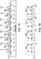
- FIG. 1A is a schematic cross-sectional view illustrating a one-bit memory cell for a nonvolatile memory according to a first example useful for the understanding of the present invention.
- the one-bit memory cell is formed on a p-substrate, and comprises a plurality of serially-connected storage units.
- serially-connected storage units For clarification and brevity, only four storage units SU1, SU2, SU3 and SU4 are shown in FIG. 1A . Of course, the number of the serially-connected storage units may be varied according to the practical requirements.
- the first storage unit SU1 comprises a first n-doped region 11, a second n-doped region 12 and a third n-doped region 13, which are formed in the surface of the p-substrate. Moreover, the first n-doped region 11 is connected to a bit line (BL). A first channel region is formed between the first n-doped region 11 and the second n-doped region 12. A first gate structure is disposed over the first channel region. A second channel region is formed between the second n-doped region 12 and the third n-doped region 13. A second gate structure is disposed over the second channel region.
- the first gate structure comprises a first gate oxide layer 14 and a first gate conductor layer 15.
- the second gate structure comprises a second gate oxide layer 16 and a second gate conductor layer 17.
- the first gate conductor layer 15 is connected to a first control signal line C1.
- the second gate conductor layer 17 is connected to a first anti-fuse signal line AF1.
- each of the other storage units SU2, SU3 and SU4 are similar to those of the first storage unit SU1. That is, the second storage unit SU2 comprises a first n-doped region 21, a second n-doped region 22, and a third n-doped region 23; the third storage unit SU3 comprises a first n-doped region 31, a second n-doped region 32, and a third n-doped region 33; and the fourth storage unit SU4 comprises a first n-doped region 41, a second n-doped region 42, and a third n-doped region 43.
- each of the storage units SU2, SU3 and SU4 has a first gate structure and a second gate structure.
- the first gate structure of the second storage unit SU2 comprises a first gate oxide layer 24 and a first gate conductor layer 25, and the second gate structure of the second storage unit SU2 comprises a second gate oxide layer 26 and a second gate conductor layer 27.
- the first gate structure of the third storage unit SU3 comprises a first gate oxide layer 34 and a first gate conductor layer 35, and the second gate structure of the third storage unit SU3 comprises a second gate oxide layer 36 and a second gate conductor layer 37.
- the first gate structure of the fourth storage unit SU4 comprises a first gate oxide layer 44 and a first gate conductor layer 45, and the second gate structure of the fourth storage unit SU4 comprises a second gate oxide layer 46 and a second gate conductor layer 47.
- the first gate conductor layer 25 is connected to a second control signal line C2, and the second gate conductor layer 27 is connected to a second anti-fuse signal line AF2.
- the first gate conductor layer 35 is connected to a third control signal line C3, and the second gate conductor layer 37 is connected to a third anti-fuse signal line AF3.
- the first gate conductor layer 45 is connected to a fourth control signal line C4, and the second gate conductor layer 47 is connected to a fourth anti-fuse signal line AF4. Please refer to FIG. 1A again.
- the third n-doped region 13 of the first storage unit SU1 and the first n-doped region 21 of the second storage unit SU2 are located adjacent to each other, so that the first storage unit SU1 and the second storage unit SU2 are connected with each other in series.
- only one n-doped region is formed, wherein a portion of this n-doped region serves as the third n-doped region 13 of the first storage unit SU1 and the other portion of this n-doped region serves as the first n-doped region 21 of the second storage unit SU2.
- the other serially-connected storage units are produced by the similar semiconductor fabricating process, and are not redundantly described herein. FIG.
- FIG. 1B is a schematic equivalent circuit of the one-bit memory cell of FIG. 1A .
- the first n-doped region 11, the second n-doped region 12 and the first gate structure of the first storage unit SU1 are collaboratively defined as a control transistor Tc.
- the second n-doped region 12, the third n-doped region 13 and the second gate structure are collaboratively defined as an anti-fuse transistor Taf.
- the control transistor Tc and the anti-fuse transistor Taf are connected with each other in series.
- each of the storage units SU2, SU3 and SU4 comprises a control transistor Tc and an anti-fuse transistor Taf, which are connected with each other in series.
- the storage unit may be considered to be in an on state or a first state.
- the anti-fuse transistor Taf may be considered to have a capacitor and a switch element, which are connected with each other in parallel. Under this circumstance, the storage unit may be considered to be in an off state or a second state.
- FIG. 2 is a schematic equivalent circuit illustrating a nonvolatile memory composed of several one-bit memory cells.
- the nonvolatile memory which acts as nand-type is composed of two or more one-bit memory cells.
- the nonvolatile memory is composed of two one-bit memory cells. Consequently, the nonvolatile memory can provide a two-bit data, including the zeroth bit data (BL0) and the first bit data (BL1).
- BL0 zeroth bit data
- BL1 first bit data
- FIG.2 is a 4 cycle sample.
- the gates of the control transistors of all first storage units are connected to the first control signal line C1, and the gates of the anti-fuse transistors of all first storage units are connected to the first anti-fuse signal line AF1.
- the gates of the control transistors of all second storage units are connected to the second control signal line C2, and the gates of the anti-fuse transistors of all second storage units are connected to the second anti-fuse signal line AF2.
- the gates of the control transistors of all third storage units are connected to the third control signal line C3, and the gates of the anti-fuse transistors of all third storage units are connected to the third anti-fuse signal line AF3.
- the gates of the control transistors of all fourth storage units are connected to the fourth control signal line C4, and the gates of the anti-fuse transistors of all fourth storage units are connected to the fourth anti-fuse signal line AF4.
- the one-bit memory cell of the present invention may be used as a multi-time programming memory (MTP memory) or a one time programming memory (OTP memory).
- MTP memory multi-time programming memory
- OTP memory one time programming memory
- FIG. 3 is flowchart illustrating a method of controlling the one-bit memory cell according to an example useful for the understanding of the present invention, in which the one-bit memory cell is used as a MTP memory. Since the one-bit memory cell is used as the MTP memory, the one-bit memory cell can be programmed and erased many times. In a case that the one-bit memory cell is composed of N serially-connected storage units, the one-bit memory cell can be programmed N times. Moreover, the storage units of the one-bit memory cell are programmed in a backward programming manner.
- Step S304 if the one-bit memory cell needs to be programmed again (Step S304), another storage unit will be programmed (Step S306).
- the one-bit memory cell is composed of four serially-connected storage units.
- the storage state (off state or on state) is recorded into the fourth storage unit. If the data of the one-bit memory cell needs to be read, the storage state of the fourth storage unit is provided.
- the storage state of the fourth storage unit is directly abandoned. That is, don't care (or ignore) the storage state of the fourth storage unit. Then, in a case that the one-bit memory cell is programmed again, the storage state (off state or on state) is recorded into the third storage unit. If the data of the one-bit memory cell needs to be read, the storage state of the third storage unit is provided.
- the storage state of the third storage unit is directly abandoned. That is, don't care the storage state of the third storage unit. Then, in a case that the one-bit memory cell is programmed again, the storage state (off state or on state) is recorded into the second storage unit. If the data of the one-bit memory cell needs to be read, the storage state of the second storage unit is provided.
- the storage state of the second storage unit is directly abandoned. That is, don't care the storage state of the second storage unit. Then, in a case that the one-bit memory cell is programmed again, the storage state (off state or on state) is recorded into the first storage unit. If the data of the one-bit memory cell needs to be read, the storage state of the first storage unit is provided.
- the one-bit memory cell can be programmed four times. That is, the one-bit memory cell of the present invention can be used as the MTP memory.
- the voltages of associated signals applied to the one-bit memory cell when the one-bit memory cell is programmed, erased or read will be illustrated in more details. It is assumed that the one-bit memory cell is produced by a standard CMOS fabricating process and the withstanding voltage of each transistor is 3.3V. If the voltage applied to a specified transistor is larger than the withstanding voltage, the gate oxide layer of the specified transistor is ruptured.
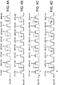
- FIGS. 4A ⁇ 4D schematically illustrate the voltages of associated signals applied to the one-bit memory cell when the one-bit memory cell is programmed and read at the first time.
- a rupture voltage (Vpp, e.g. 6V, which is varied according to the process generation) is provided to only the fourth anti-fuse signal line AF4.
- An on voltage (Vpp/2, e.g. 3V) is provided to the control signal lines C1 ⁇ C4 and the anti-fuse signal lines AF1 ⁇ AF3.
- a programmed voltage (e.g. 0V) is provided to the bit line BL.
- the gate oxide layer of the anti-fuse transistor in the fourth storage unit is ruptured. Consequently, the both ends of the capacitor in the fourth storage unit have low impedance. As shown in Fig. 4A , the capacitor is replaced by a resistor when the on state is recorded into the fourth storage unit. Under this circumstance, the fourth storage unit is considered to be in the on state or the first state.
- a rupture voltage e.g. 6V
- An on voltage e.g. 3V
- a non-programmed voltage e.g. 3V
- the gate oxide layer of the anti-fuse transistor in the fourth storage unit is not ruptured. Consequently, the both ends of the capacitor in the fourth storage unit have high impedance.
- the fourth storage unit is considered to be in the off state or the second state.
- the non-programmed voltage (e.g. 3V) provided to the bit line BL is also called as the program inhibition. That is to say, when the non-programmed voltage (e.g. 3V) is provided to the bit line BL in program inhibition, the prior programmed storage unit (in the on state or off state) is maintained and will not be influenced or programmed again.
- the one-bit memory cell is read.
- a read control voltage e.g. 1V
- a bit line reading voltage e.g. 0V
- the voltage provided to the control signal lines C1 ⁇ C4 and the anti-fuse signal lines AF1 ⁇ AF4 is the read control voltage (e.g.1V) when reading the one-bit memory cell.
- the voltages provided to the control signal lines C1 ⁇ C4 and the anti-fuse signal lines AF1 ⁇ AF4 could be different.
- a first read control voltage e.g.1V
- a second read control voltage e.g. 1.2V
- the one-bit memory cell is read.
- a read control voltage e.g. 1V
- a bit line reading voltage e.g. 0V
- a tiny reading current Ir may flow from the fourth anti-fuse signal line AF4 to the bit line BL.
- the off state i.e. the second state of the one-bit memory cell is detected.
- the storage state of the fourth storage unit is directly abandoned. Then, regardless of whether the one-bit memory cell is programmed or read, an off voltage (e.g. 0V) is provided to the fourth control signal line C4 and the fourth anti-fuse signal line AF4. Consequently, the subsequent programming actions and reading actions are not influenced by the storage state of the fourth storage unit.
- an off voltage e.g. 0V
- FIGS. 5A ⁇ 5D schematically illustrate the voltages of associated signals applied to the one-bit memory cell when the one-bit memory cell is programmed and read at the second time.
- a rupture voltage e.g. 6V
- An on voltage e.g. 3V
- a programmed voltage e.g. 0V
- the both ends of the capacitor in the third storage unit have low impedance.
- the third storage unit is considered to be in the on state or the first state.
- the off voltage (0V) is provided to the control signal line C4, the second program action is not influenced by the storage state of the fourth storage unit.
- a rupture voltage (e.g. 6V) is provided to only the third anti-fuse signal line AF3.
- An on voltage e.g. 3V
- a non-programmed voltage (e.g. 3V) is provided to the bit line BL.
- the third storage unit is considered to be in the off state or the second state.
- the non-programmed voltage e.g. 3V
- the bit line BL is capable of protecting the prior programmed storage unit from being programmed again in the program inhibition.
- the one-bit memory cell is read.
- a read control voltage e.g. 1V
- a bit line reading voltage e.g. 0V
- a larger reading current Ir may flow from the third anti-fuse signal line AF3 to the bit line BL. After the reading current Ir is sensed by a sense amplifier (not shown), the on state (i.e. the first state) of the one-bit memory cell is detected.
- the one-bit memory cell is read.
- a read control voltage e.g. 1V
- a bit line reading voltage e.g. 0V
- a tiny reading current Ir may flow from the third anti-fuse signal line AF3 to the bit line BL.
- the off state i.e. the second state of the one-bit memory cell is detected.
- the storage state of the third storage unit is directly abandoned. Then, regardless of whether the one-bit memory cell is programmed or read, an off voltage (e.g. 0V) is provided to the control signal lines C3 ⁇ C4 and the anti-fuse signal lines AF3 ⁇ AF4. Consequently, the subsequent programming actions and reading actions are not influenced by the storage states of the third storage unit and the fourth storage unit.
- an off voltage e.g. 0V
- FIGS. 6A ⁇ 6D schematically illustrate the voltages of associated signals applied to the one-bit memory cell when the one-bit memory cell is programmed and read at the third time.
- a rupture voltage e.g. 6V
- An on voltage e.g. 3V
- a programmed voltage e.g. 0V
- the gate oxide layer of the anti-fuse transistor in the second storage unit is ruptured. Consequently, the both ends of the capacitor in the second storage unit have low impedance. Under this circumstance, the second storage unit is considered to be in the on state or the first state.
- a rupture voltage (e.g. 6V) is provided to only the second anti-fuse signal line AF2.
- An on voltage e.g. 3V
- a non-programmed voltage (e.g. 3V) is provided to the bit line BL.
- the one-bit memory cell is read.
- a read control voltage e.g. 1V
- a bit line reading voltage e.g. 0V
- a larger reading current Ir may flow from the second anti-fuse signal line AF2 to the bit line BL. After the reading current Ir is sensed by a sense amplifier (not shown), the on state (i.e. the first state) of the one-bit memory cell is detected.
- the one-bit memory cell is read.
- a read control voltage e.g. 1V
- a bit line reading voltage e.g. 0V
- a tiny reading current Ir may flow from the second anti-fuse signal line AF2 to the bit line BL.
- the off state i.e. the second state of the one-bit memory cell is detected.
- the storage state of the second storage unit is directly abandoned. Then, regardless of whether the one-bit memory cell is programmed or read, an off voltage (e.g. 0V) to the control signal lines C2 ⁇ C4 and the anti-fuse signal lines AF2 ⁇ AF4. Consequently, the subsequent programming actions and reading actions are not influenced by the storage states of the second, third storage and fourth storage units.
- an off voltage e.g. 0V
- FIGS. 7A ⁇ 7D schematically illustrate the voltages of associated signals applied to the one-bit memory cell when the one-bit memory cell is programmed and read at the fourth time.
- a rupture voltage e.g. 6V
- An on voltage e.g. 3V
- a programmed voltage e.g. 0V
- the gate oxide layer of the anti-fuse transistor in the first storage unit is ruptured. Consequently, the both ends of the capacitor in the first storage unit have low impedance. Under this circumstance, the first storage unit is considered to be in the on state or the first state.
- a rupture voltage e.g. 6V
- An on voltage e.g. 3V
- a non-programmed voltage e.g. 3V
- the gate oxide layer of the anti-fuse transistor in the first storage unit is not ruptured. Consequently, the both ends of the capacitor in the first storage unit have high impedance. Under this circumstance, the first storage unit is considered to be in the off state or the second state.
- the one-bit memory cell is read.
- a read control voltage e.g. 1V
- a bit line reading voltage e.g. 0V
- a larger reading current Ir may flow from the first anti-fuse signal line AF1 to the bit line BL. After the reading current Ir is sensed by a sense amplifier (not shown), the on state (i.e. the first state) of the one-bit memory cell is detected.
- the one-bit memory cell is read.
- a read control voltage e.g. 1V
- a bit line reading voltage e.g. 0V
- a tiny reading current Ir may flow from the first anti-fuse signal line AF1 to the bit line BL.
- the off state i.e. the second state of the one-bit memory cell is detected.
- the one-bit memory cell of the present invention may be applied to a nonvolatile memory and have the function of the MTP memory.
- the one-bit memory cell of the present invention may be used as a one time programming memory (OTP memory).
- OTP memory one time programming memory
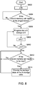
- FIG. 8 is flowchart illustrating a method of controlling the one-bit memory cell according to an embodiment of the present invention, in which the one-bit memory cell is used as an OTP memory. Since the one-bit memory cell is used as the OTP memory, the one-bit memory cell can be programmed once and cannot be erased. In a case that the one-bit memory cell is composed of N serially-connected storage units, for programming the one-bit memory cell, an identical storage state is recorded into all of the N storage units in a backward programming manner.
- the steps S806, S808 and S810 are employed to sequentially record the storage state in N storage units in N program cycles.
- Step S812 the storage state of the N storage units is provided simultaneously.
- the one-bit memory cell is composed of four serially-connected storage units.
- the storage state (off state or on state) is recorded into the all of the four storage units. If the data of the one-bit memory cell needs to be read, the identical storage state of the four storage units is provided simultaneously.
- the voltages of associated signals applied to the one-bit memory cell when the one-bit memory cell is programmed or read will be illustrated in more details. It is assumed that the one-bit memory cell is produced by a standard CMOS fabricating process and the withstanding voltage of each transistor is 3.3V. If the voltage applied to a specified transistor is larger than the withstanding voltage, the gate oxide layer of the specified transistor is ruptured.
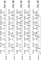
- FIGS. 9A ⁇ 9E schematically illustrate the voltages of associated signals applied to the one-bit memory cell when the one-bit memory cell is programmed and read in an on state.
- the on state i.e. the first state
- the on state i.e. the first state
- a rupture voltage e.g. 6V
- An on voltage e.g. 3V
- a programmed voltage e.g. 0V
- the gate oxide layer of the anti-fuse transistor in the fourth storage unit is ruptured. Consequently, the both ends of the capacitor in the fourth storage unit have low impedance. Under this circumstance, the fourth storage unit is considered to be in the on state or the first state.
- the on state i.e. the first state
- an off voltage e.g. 0V
- a rupture voltage e.g. 6V
- An on voltage e.g. 3V
- a programmed voltage e.g. 0V
- the third storage unit is considered to be in the on state or the first state.
- the on state i.e. the first state
- an off voltage e.g. 0V
- a rupture voltage e.g. 6V
- An on voltage e.g. 3V
- a programmed voltage e.g. 0V
- BL bit line
- the second storage unit is considered to be in the on state or the first state.
- the on state i.e. the first state
- an off voltage e.g. 0V
- a rupture voltage e.g. 6V
- An on voltage e.g. 3V
- a programmed voltage e.g. 0V
- a read control voltage (e.g. 1V) is provided to the control signal lines C1 ⁇ C4 and the anti-fuse signal lines AF1 ⁇ AF4.
- a bit line reading voltage (e.g. 0V) is provided to the bit line BL.
- the on state (i.e. the first state) of the one-bit memory cell is detected.
- the voltage provided to the control signal lines C1 ⁇ C4 and the anti-fuse signal lines AF1 ⁇ AF4 is the read control voltage (e.g.1V) when reading the one-bit memory cell.
- the voltages provided to the control signal lines C1 ⁇ C4 and the anti-fuse signal lines AF1 ⁇ AF4 could be different.
- a first read control voltage e.g.1V
- a second read control voltage e.g. 1.2V
- the one-bit memory cell of the present invention is used as the OTP memory.
- the one-bit memory cell may be considered to be in the on state (i.e. the first state) according to the reading current. Consequently, even if the semiconductor fabricating process is subject to deviation and the gate oxide layer fails to be successfully ruptured during some program periods, the storage state of the one-bit memory cell can be accurately judged.
- FIGS. 10A ⁇ 10E schematically illustrate the voltages of associated signals applied to the one-bit memory cell when the one-bit memory cell is programmed and read in an off state.
- the off state i.e. the second state
- a rupture voltage is provided to only the fourth anti-fuse signal line AF4 (e.g. 6V).
- An on voltage e.g. 3V
- a non-programmed voltage e.g. 3V
- the gate oxide layer of the anti-fuse transistor in the fourth storage unit is not ruptured. Consequently, the both ends of the capacitor in the fourth storage unit have high impedance. Under this circumstance, the fourth storage unit is considered to be in the off state or the second state.
- the off state (i.e. the second state) is recorded into the third storage unit.
- an off voltage e.g. 0V
- a rupture voltage e.g. 6V
- An on voltage e.g. 3V
- a non-programmed voltage e.g. 3V
- the gate oxide layer of the anti-fuse transistor in the third storage unit is not ruptured. Consequently, the both ends of the capacitor in the third storage unit have high impedance. Under this circumstance, the third storage unit is considered to be in the off state or the second state.
- the off state (i.e. the second state) is recorded into the second storage unit.
- an off voltage e.g. 0V
- a rupture voltage e.g. 6V
- An on voltage e.g. 3V
- a non-programmed voltage e.g. 3V
- the gate oxide layer of the anti-fuse transistor in the second storage unit is not ruptured. Consequently, the both ends of the capacitor in the second storage unit have high impedance. Under this circumstance, the second storage unit is considered to be in the off state or the second state.
- the off state (i.e. the second state) is recorded into the first storage unit.
- an off voltage e.g. 0V
- a rupture voltage e.g. 6V
- An on voltage e.g. 3V
- a non-programmed voltage e.g. 3V
- the gate oxide layer of the anti-fuse transistor in the first storage unit is not ruptured. Consequently, the both ends of the capacitor in the first storage unit have high impedance. Under this circumstance, the first storage unit is considered to be in the off state or the second state.
- a read control voltage (e.g. 1V) is provided to the control signal lines C1 ⁇ C4 and the anti-fuse signal lines AF1 ⁇ AF4.
- a bit line reading voltage (e.g. 0V) is provided to the bit line BL.
- the reading current Ir is also very low. After the reading current Ir is sensed by a sense amplifier (not shown), the off state (i.e. the second state) of the one-bit memory cell is detected.
- the one-bit memory cell of the present invention may be applied to a nonvolatile memory and have the function of the OTP memory.
- FIG. 11 is a schematic cross-sectional view illustrating a one-bit memory cell for a nonvolatile memory according to a second example useful for the understanding of the present invention. Except that the first gate oxide layers 14', 24', 34' and 44' are respectively thicker than the second gate oxide layers 16', 26', 36' and 46', the configurations of the storage units SU1, SU2, SU3 and SU4 of FIG. 11 are substantially identical to those of FIG. 1A . Consequently, during the process of programming the storage unit, the rupture voltage may be reduced or the second gate oxide layer 16', 26', 36' and 46'may be ruptured more easily.
- FIG. 12 is a schematic cross-sectional view illustrating a one-bit memory cell for a nonvolatile memory according to an embodiment of the present invention. Since the storage units SU1, SU2, SU3 and SU4 have identical configurations, only the first storage unit SU1 will be illustrated as follows.
- the first storage unit SU1 comprises a first n-doped region 91 and a second n-doped region 92, which are formed in the surface of a p-substrate. Moreover, the first n-doped region 91 is connected to a bit line (BL). A channel region is formed between the first n-doped region 91 and the second n-doped region 92. A gate structure is disposed over the channel region.
- the gate structure comprises a gate oxide layer and a gate conductor layer 98.
- the gate oxide layer comprises a first part 95 and a second part 96, wherein the first part 95 is thicker than the second part 96.
- the gate conductor layer 98 is formed over the first part 95 and the second part 96 of the gate oxide layer.
- a first control signal line C1 is connected to the portion of the gate conductor layer 98 overlying the first part 95 of the gate oxide layer.
- a first anti-fuse signal line AF1 is connected to the portion of the gate conductor layer 98 overlying the second part 96 of the gate oxide layer.
- the storage unit is implemented by a single transistor.
- the first part 95 of the gate oxide layer and the gate conductor layer 98 are collaboratively functioned as a first gate structure of the control transistor.
- the second part 96 of the gate oxide layer and the gate conductor layer 98 are collaboratively functioned as the second gate structure of an anti-fuse transistor.
- the one-bit memory cell of the embodiment may also be used an OTP memory or a MTP memory.
- the controlling mechanism of the one-bit memory cell of the embodiment is similar to that of the first example, and is not redundantly described herein.
- all storage units of the one-bit memory cell have identical configurations.
- the configuration of the last storage unit of the serially-connected storage units is different from the configurations of other storage units.
- FIG. 13 is a schematic cross-sectional view illustrating a one-bit memory cell for a nonvolatile memory according to a third example useful for the understanding of the present invention.
- the last storage unit SU5 has no third n-doped region.
- the third n-doped region is replaced by an isolation structure 53.
- the isolation structure 53 is a shallow trench isolation (STI) structure.
- the fifth storage unit SU5 comprises a first n-doped region 51, a second n-doped region 52 and the isolation structure 53, which are formed in the surface of a p-substrate.
- a first channel region is formed between the first n-doped region 51 and the second n-doped region 52.
- a first gate structure is disposed over the first channel region.
- a third channel region is formed between the second n-doped region 52 and the isolation structure 53.
- a second gate structure is disposed over the third channel region.
- the first gate structure comprises a first gate oxide layer 54 and a first gate conductor layer 55.
- the second gate structure comprises a second gate oxide layer 56 and a second gate conductor layer 57.
- the first gate conductor layer 55 is connected to a fifth control signal line C5.
- the second gate conductor layer 57 is connected to a fifth anti-fuse signal line AF5.
- the concepts of the third example may be combined with the concepts of the other examples and/or the embodiment.
- the third n-doped region of the last storage unit of the one-bit memory cell may be replaced by an isolation structure.
- the second n-doped region of the last storage unit of the one-bit memory cell may be replaced by an isolation structure.
Landscapes
- Read Only Memory (AREA)
- Semiconductor Memories (AREA)
- Non-Volatile Memory (AREA)
Claims (3)
- Mémoire non volatile comprenant une première cellule de mémoire d'un bit, dans laquelle la première cellule de mémoire d'un bit est formée sur un substrat, et la première cellule de mémoire d'un bit comprend :une première ligne de bit (BL) ; etN unités de stockage (SU1, SU2, SU3, SU4), dans laquelle chacune des N unités de stockage (SU1, SU2, SU3, SU4) comprend une première région dopée (91) et une seconde région dopée (92), qui sont formées dans une surface du substrat, dans laquelle une structure de grille est disposée par-dessus une région de canal entre la première région dopée (91) et la seconde région dopée (92), dans laquelle la structure de grille comprend une couche d'oxyde de grille et une couche de conducteur de grille (98), dans laquelle la couche d'oxyde de grille comprend une première partie (95) et une seconde partie (96), la première partie (95) est plus épaisse que la seconde partie (96), et la couche de conducteur de grille (98) est formée par-dessus la couche d'oxyde de grille,dans laquelle la première région dopée (91) de la première unité de stockage (SU1) est connectée à la première ligne de bit (BL), et la structure de grille de la première unité de stockage (SU1) est connectée à une première ligne de signal de commande (CL1) et une première ligne de signal anti-fusion (AF1), dans laquelle la première région dopée (91) de la mième unité de stockage est connectée à la seconde région dopée (92) de la (m-1)ième unité de stockage, et la structure de grille de la mième unité de stockage est connectée à une mième ligne de signal de commande et une mième ligne de signal anti-fusion, dans laquelle m est un nombre entier supérieur ou égal à 2 et inférieur ou égal à N.
- Mémoire non volatile selon la revendication 1, dans laquelle la première cellule de mémoire d'un bit comprend en outre une (N+1)ième unité de stockage, dans laquelle la (N+1)ième unité de stockage comprend la première région dopée (91) et une structure d'isolation, qui sont formées dans la surface du substrat, dans laquelle la structure de grille de la (N+1)ième unité de stockage est disposée par-dessus une autre région de canal entre la première région dopée (91) et la structure d'isolation de la (N+1)ième unité de stockage, dans laquelle la structure de grille de la (N+1)ième unité de stockage est connectée à une (N+1)ième ligne de signal de commande et une (N+1)ième ligne de signal anti-fusion, et la première région dopée (91) de la (N+1)ième unité de stockage est connectée à la seconde région dopée (92) de la Nième unité de stockage.
- Procédé de commande d'une cellule de mémoire d'un bit d'une mémoire non volatile, la cellule de mémoire d'un bit comprenant une ligne de bit et N unités de stockage (SU1, SU2, SU3, SU4), les N unités de stockage (SU1, SU2, SU3, SU4) étant connectées les unes aux autres en série, la ligne de bit étant connectée à une première unité de stockage des N unités de stockage (SU1, SU2, SU3, SU4), le procédé comprenant les étapes de :(a) si la cellule de mémoire d'un bit doit être programmée, programmation séquentielle des N unités de stockage (SU1, SU2, SU3, SU4) dans N cycles de programme, de sorte qu'un état de stockage soit enregistré dans la totalité des N unités de stockage (SU1, SU2, SU3, SU4) ; et(b) si la cellule de mémoire d'un bit doit être lue, fourniture simultanée de l'état de stockage des N unités de stockage (SU1, SU2, SU3, SU4).
Applications Claiming Priority (1)
| Application Number | Priority Date | Filing Date | Title |
|---|---|---|---|
| US13/590,392 US8681528B2 (en) | 2012-08-21 | 2012-08-21 | One-bit memory cell for nonvolatile memory and associated controlling method |
Publications (3)
| Publication Number | Publication Date |
|---|---|
| EP2701155A2 EP2701155A2 (fr) | 2014-02-26 |
| EP2701155A3 EP2701155A3 (fr) | 2018-01-10 |
| EP2701155B1 true EP2701155B1 (fr) | 2019-01-09 |
Family
ID=47215422
Family Applications (2)
| Application Number | Title | Priority Date | Filing Date |
|---|---|---|---|
| EP12192992.1A Active EP2701156B1 (fr) | 2012-08-21 | 2012-11-16 | Cellule de mémoire à un bit pour mémoire non volatile et procédé de commande associé |
| EP12192973.1A Active EP2701155B1 (fr) | 2012-08-21 | 2012-11-16 | Cellule de mémoire à un bit pour mémoire non volatile et procédé de commande associé |
Family Applications Before (1)
| Application Number | Title | Priority Date | Filing Date |
|---|---|---|---|
| EP12192992.1A Active EP2701156B1 (fr) | 2012-08-21 | 2012-11-16 | Cellule de mémoire à un bit pour mémoire non volatile et procédé de commande associé |
Country Status (5)
| Country | Link |
|---|---|
| US (1) | US8681528B2 (fr) |
| EP (2) | EP2701156B1 (fr) |
| JP (1) | JP5492285B2 (fr) |
| CN (2) | CN103633095B (fr) |
| TW (2) | TWI496154B (fr) |
Families Citing this family (14)
| Publication number | Priority date | Publication date | Assignee | Title |
|---|---|---|---|---|
| US9166149B2 (en) * | 2012-11-27 | 2015-10-20 | Industrial Technology Research Institute | Magnetic device with a substrate, a sensing block and a repair layer |
| US9281074B2 (en) * | 2013-05-16 | 2016-03-08 | Ememory Technology Inc. | One time programmable memory cell capable of reducing leakage current and preventing slow bit response |
| US9601499B2 (en) | 2013-05-16 | 2017-03-21 | Ememory Technology Inc. | One-time programmable memory cell capable of reducing leakage current and preventing slow bit response, and method for programming a memory array comprising the same |
| US9508396B2 (en) * | 2014-04-02 | 2016-11-29 | Ememory Technology Inc. | Array structure of single-ploy nonvolatile memory |
| JP6345107B2 (ja) * | 2014-12-25 | 2018-06-20 | ルネサスエレクトロニクス株式会社 | 半導体装置およびその製造方法 |
| US9799662B2 (en) * | 2015-08-18 | 2017-10-24 | Ememory Technology Inc. | Antifuse-type one time programming memory cell and array structure with same |
| US9620176B2 (en) * | 2015-09-10 | 2017-04-11 | Ememory Technology Inc. | One-time programmable memory array having small chip area |
| US9613714B1 (en) * | 2016-01-19 | 2017-04-04 | Ememory Technology Inc. | One time programming memory cell and memory array for physically unclonable function technology and associated random code generating method |
| KR102506838B1 (ko) * | 2016-09-30 | 2023-03-08 | 에스케이하이닉스 주식회사 | 반도체 장치 및 그의 동작 방법 |
| US9882566B1 (en) * | 2017-01-10 | 2018-01-30 | Ememory Technology Inc. | Driving circuit for non-volatile memory |
| US11152380B2 (en) * | 2019-08-06 | 2021-10-19 | Globalfoundries Singapore Pte. Ltd. | Memory device and a method for forming the memory device |
| US11217595B2 (en) * | 2020-01-15 | 2022-01-04 | Zhuhai Chuangfeixin Technology Co., Ltd. | Antifuse OTP structure with hybrid device and hybrid junction for select transistor |
| KR102862023B1 (ko) | 2022-07-08 | 2025-09-19 | 창신 메모리 테크놀로지즈 아이엔씨 | 반도체 구조, 메모리 및 그 작동 방법 |
| CN117425344A (zh) * | 2022-07-08 | 2024-01-19 | 长鑫存储技术有限公司 | 半导体结构、存储器及其操作方法 |
Family Cites Families (19)
| Publication number | Priority date | Publication date | Assignee | Title |
|---|---|---|---|---|
| US5469396A (en) * | 1994-06-07 | 1995-11-21 | Actel Corporation | Apparatus and method determining the resistance of antifuses in an array |
| US7157314B2 (en) * | 1998-11-16 | 2007-01-02 | Sandisk Corporation | Vertically stacked field programmable nonvolatile memory and method of fabrication |
| JP2002279787A (ja) * | 2001-03-16 | 2002-09-27 | Hitachi Ltd | 不揮発性半導体記憶装置 |
| US6791891B1 (en) | 2003-04-02 | 2004-09-14 | Kilopass Technologies, Inc. | Method of testing the thin oxide of a semiconductor memory cell that uses breakdown voltage |
| KR100558486B1 (ko) * | 2003-07-14 | 2006-03-07 | 삼성전자주식회사 | 비휘발성 반도체 메모리 장치 및 이 장치의 원 타임프로그래밍 제어방법 |
| JP2005116048A (ja) * | 2003-10-07 | 2005-04-28 | Elpida Memory Inc | アンチフューズプログラミング回路 |
| TWI227501B (en) * | 2004-04-14 | 2005-02-01 | Novatek Microelectronics Corp | Apparatus and method for reprogramming by using one-time programming element |
| WO2005109516A1 (fr) | 2004-05-06 | 2005-11-17 | Sidense Corp. | Architecture de reseau de transistors anti-fusibles a canaux partages |
| TWI293757B (en) * | 2004-05-27 | 2008-02-21 | Novatek Microelectronics Corp | Apparatus and method for reprogramming by using one-time programming element |
| US8014199B2 (en) * | 2006-05-22 | 2011-09-06 | Spansion Llc | Memory system with switch element |
| JP2008198304A (ja) * | 2007-02-15 | 2008-08-28 | Toshiba Corp | 不揮発性半導体記憶装置 |
| TW200836323A (en) * | 2007-02-27 | 2008-09-01 | Ememory Technology Inc | Apparatus and method for trimming integrated circuit |
| US7800156B2 (en) * | 2008-02-25 | 2010-09-21 | Tower Semiconductor Ltd. | Asymmetric single poly NMOS non-volatile memory cell |
| US20090283814A1 (en) * | 2008-05-19 | 2009-11-19 | Hsin-Ming Chen | Single-poly non-volatile memory cell |
| US8344445B2 (en) * | 2009-07-30 | 2013-01-01 | Ememory Technology Inc. | Non-volatile semiconductor memory cell with dual functions |
| KR101884031B1 (ko) * | 2010-04-07 | 2018-07-31 | 가부시키가이샤 한도오따이 에네루기 켄큐쇼 | 반도체 기억 장치 |
| US8283731B2 (en) * | 2010-06-02 | 2012-10-09 | Kilopass Technologies, Inc. | One-time programmable memory |
| TW201203253A (en) * | 2010-07-06 | 2012-01-16 | Maxchip Electronics Corp | One time programmable memory and the manufacturing method and operation method thereof |
| CN102324428B (zh) * | 2011-08-02 | 2013-11-27 | 长沙艾尔丰华电子科技有限公司 | 一次可编程存储单元及其制造方法和一次可编程存储阵列 |
-
2012
- 2012-08-21 US US13/590,392 patent/US8681528B2/en active Active
- 2012-11-16 EP EP12192992.1A patent/EP2701156B1/fr active Active
- 2012-11-16 EP EP12192973.1A patent/EP2701155B1/fr active Active
- 2012-12-12 TW TW101146978A patent/TWI496154B/zh active
- 2012-12-12 TW TW104113879A patent/TWI560717B/zh active
- 2012-12-25 CN CN201210571629.2A patent/CN103633095B/zh active Active
- 2012-12-25 CN CN201510696096.4A patent/CN105405467B/zh active Active
- 2012-12-26 JP JP2012282856A patent/JP5492285B2/ja active Active
Non-Patent Citations (1)
| Title |
|---|
| None * |
Also Published As
| Publication number | Publication date |
|---|---|
| EP2701155A2 (fr) | 2014-02-26 |
| TW201409478A (zh) | 2014-03-01 |
| CN105405467A (zh) | 2016-03-16 |
| TWI496154B (zh) | 2015-08-11 |
| CN105405467B (zh) | 2019-04-19 |
| EP2701155A3 (fr) | 2018-01-10 |
| EP2701156A2 (fr) | 2014-02-26 |
| EP2701156B1 (fr) | 2019-01-16 |
| JP5492285B2 (ja) | 2014-05-14 |
| CN103633095B (zh) | 2016-04-13 |
| TW201530548A (zh) | 2015-08-01 |
| CN103633095A (zh) | 2014-03-12 |
| TWI560717B (en) | 2016-12-01 |
| JP2014041684A (ja) | 2014-03-06 |
| US20140056051A1 (en) | 2014-02-27 |
| US8681528B2 (en) | 2014-03-25 |
| EP2701156A3 (fr) | 2018-01-10 |
Similar Documents
| Publication | Publication Date | Title |
|---|---|---|
| EP2701155B1 (fr) | Cellule de mémoire à un bit pour mémoire non volatile et procédé de commande associé | |
| EP3614387B1 (fr) | Cellule de mémoire de programmation en une seule fois et grille de mémoire pour technologie de fonction physiquement inclonable et procédé de génération de code aléatoire associé | |
| US9431111B2 (en) | One time programming memory cell, array structure and operating method thereof | |
| US9224497B2 (en) | One time programmable memory cell capable of reducing leakage current and preventing slow bit response | |
| US9087588B2 (en) | Programmable non-volatile memory | |
| US8045414B2 (en) | Non-volatile semiconductor memory device | |
| US9799662B2 (en) | Antifuse-type one time programming memory cell and array structure with same | |
| KR102178025B1 (ko) | 감소된 레이아웃 면적을 갖는 otp 셀 | |
| US10783960B2 (en) | Non-volatile memory cell and non-volatile cell array | |
| US20170148801A1 (en) | Antifuse-type one time programming memory cell and array structure with same | |
| US9502426B1 (en) | One time programming non-volatile memory cell | |
| TW201140602A (en) | Antifuse programmable memory array | |
| KR101958518B1 (ko) | 프로그래밍의 신뢰성이 개선된 otp 셀 | |
| CN109313924B (zh) | 减少非易失性存储器单元阵列中的编程干扰的方法和设备 | |
| JPH1083683A (ja) | 不揮発性半導体メモリ装置 | |
| US9136217B2 (en) | One-time programmable memory cell | |
| JP2013197741A (ja) | プログラマブルロジックデバイス | |
| US9058891B2 (en) | EEPROM cell and EEPROM device |
Legal Events
| Date | Code | Title | Description |
|---|---|---|---|
| PUAI | Public reference made under article 153(3) epc to a published international application that has entered the european phase |
Free format text: ORIGINAL CODE: 0009012 |
|
| AK | Designated contracting states |
Kind code of ref document: A2 Designated state(s): AL AT BE BG CH CY CZ DE DK EE ES FI FR GB GR HR HU IE IS IT LI LT LU LV MC MK MT NL NO PL PT RO RS SE SI SK SM TR |
|
| AX | Request for extension of the european patent |
Extension state: BA ME |
|
| PUAL | Search report despatched |
Free format text: ORIGINAL CODE: 0009013 |
|
| AK | Designated contracting states |
Kind code of ref document: A3 Designated state(s): AL AT BE BG CH CY CZ DE DK EE ES FI FR GB GR HR HU IE IS IT LI LT LU LV MC MK MT NL NO PL PT RO RS SE SI SK SM TR |
|
| AX | Request for extension of the european patent |
Extension state: BA ME |
|
| RIC1 | Information provided on ipc code assigned before grant |
Ipc: G11C 17/16 20060101AFI20171204BHEP Ipc: H01L 23/525 20060101ALI20171204BHEP |
|
| STAA | Information on the status of an ep patent application or granted ep patent |
Free format text: STATUS: REQUEST FOR EXAMINATION WAS MADE |
|
| 17P | Request for examination filed |
Effective date: 20180709 |
|
| RBV | Designated contracting states (corrected) |
Designated state(s): AL AT BE BG CH CY CZ DE DK EE ES FI FR GB GR HR HU IE IS IT LI LT LU LV MC MK MT NL NO PL PT RO RS SE SI SK SM TR |
|
| GRAP | Despatch of communication of intention to grant a patent |
Free format text: ORIGINAL CODE: EPIDOSNIGR1 |
|
| STAA | Information on the status of an ep patent application or granted ep patent |
Free format text: STATUS: GRANT OF PATENT IS INTENDED |
|
| INTG | Intention to grant announced |
Effective date: 20180907 |
|
| GRAS | Grant fee paid |
Free format text: ORIGINAL CODE: EPIDOSNIGR3 |
|
| GRAA | (expected) grant |
Free format text: ORIGINAL CODE: 0009210 |
|
| STAA | Information on the status of an ep patent application or granted ep patent |
Free format text: STATUS: THE PATENT HAS BEEN GRANTED |
|
| AK | Designated contracting states |
Kind code of ref document: B1 Designated state(s): AL AT BE BG CH CY CZ DE DK EE ES FI FR GB GR HR HU IE IS IT LI LT LU LV MC MK MT NL NO PL PT RO RS SE SI SK SM TR |
|
| REG | Reference to a national code |
Ref country code: GB Ref legal event code: FG4D |
|
| REG | Reference to a national code |
Ref country code: CH Ref legal event code: EP Ref country code: AT Ref legal event code: REF Ref document number: 1088313 Country of ref document: AT Kind code of ref document: T Effective date: 20190115 |
|
| REG | Reference to a national code |
Ref country code: DE Ref legal event code: R096 Ref document number: 602012055645 Country of ref document: DE |
|
| REG | Reference to a national code |
Ref country code: IE Ref legal event code: FG4D |
|
| REG | Reference to a national code |
Ref country code: NL Ref legal event code: MP Effective date: 20190109 |
|
| REG | Reference to a national code |
Ref country code: LT Ref legal event code: MG4D |
|
| PG25 | Lapsed in a contracting state [announced via postgrant information from national office to epo] |
Ref country code: NL Free format text: LAPSE BECAUSE OF FAILURE TO SUBMIT A TRANSLATION OF THE DESCRIPTION OR TO PAY THE FEE WITHIN THE PRESCRIBED TIME-LIMIT Effective date: 20190109 |
|
| REG | Reference to a national code |
Ref country code: AT Ref legal event code: MK05 Ref document number: 1088313 Country of ref document: AT Kind code of ref document: T Effective date: 20190109 |
|
| PG25 | Lapsed in a contracting state [announced via postgrant information from national office to epo] |
Ref country code: NO Free format text: LAPSE BECAUSE OF FAILURE TO SUBMIT A TRANSLATION OF THE DESCRIPTION OR TO PAY THE FEE WITHIN THE PRESCRIBED TIME-LIMIT Effective date: 20190409 Ref country code: PL Free format text: LAPSE BECAUSE OF FAILURE TO SUBMIT A TRANSLATION OF THE DESCRIPTION OR TO PAY THE FEE WITHIN THE PRESCRIBED TIME-LIMIT Effective date: 20190109 Ref country code: ES Free format text: LAPSE BECAUSE OF FAILURE TO SUBMIT A TRANSLATION OF THE DESCRIPTION OR TO PAY THE FEE WITHIN THE PRESCRIBED TIME-LIMIT Effective date: 20190109 Ref country code: LT Free format text: LAPSE BECAUSE OF FAILURE TO SUBMIT A TRANSLATION OF THE DESCRIPTION OR TO PAY THE FEE WITHIN THE PRESCRIBED TIME-LIMIT Effective date: 20190109 Ref country code: SE Free format text: LAPSE BECAUSE OF FAILURE TO SUBMIT A TRANSLATION OF THE DESCRIPTION OR TO PAY THE FEE WITHIN THE PRESCRIBED TIME-LIMIT Effective date: 20190109 Ref country code: PT Free format text: LAPSE BECAUSE OF FAILURE TO SUBMIT A TRANSLATION OF THE DESCRIPTION OR TO PAY THE FEE WITHIN THE PRESCRIBED TIME-LIMIT Effective date: 20190509 Ref country code: FI Free format text: LAPSE BECAUSE OF FAILURE TO SUBMIT A TRANSLATION OF THE DESCRIPTION OR TO PAY THE FEE WITHIN THE PRESCRIBED TIME-LIMIT Effective date: 20190109 |
|
| PG25 | Lapsed in a contracting state [announced via postgrant information from national office to epo] |
Ref country code: HR Free format text: LAPSE BECAUSE OF FAILURE TO SUBMIT A TRANSLATION OF THE DESCRIPTION OR TO PAY THE FEE WITHIN THE PRESCRIBED TIME-LIMIT Effective date: 20190109 Ref country code: LV Free format text: LAPSE BECAUSE OF FAILURE TO SUBMIT A TRANSLATION OF THE DESCRIPTION OR TO PAY THE FEE WITHIN THE PRESCRIBED TIME-LIMIT Effective date: 20190109 Ref country code: GR Free format text: LAPSE BECAUSE OF FAILURE TO SUBMIT A TRANSLATION OF THE DESCRIPTION OR TO PAY THE FEE WITHIN THE PRESCRIBED TIME-LIMIT Effective date: 20190410 Ref country code: BG Free format text: LAPSE BECAUSE OF FAILURE TO SUBMIT A TRANSLATION OF THE DESCRIPTION OR TO PAY THE FEE WITHIN THE PRESCRIBED TIME-LIMIT Effective date: 20190409 Ref country code: RS Free format text: LAPSE BECAUSE OF FAILURE TO SUBMIT A TRANSLATION OF THE DESCRIPTION OR TO PAY THE FEE WITHIN THE PRESCRIBED TIME-LIMIT Effective date: 20190109 Ref country code: IS Free format text: LAPSE BECAUSE OF FAILURE TO SUBMIT A TRANSLATION OF THE DESCRIPTION OR TO PAY THE FEE WITHIN THE PRESCRIBED TIME-LIMIT Effective date: 20190509 |
|
| REG | Reference to a national code |
Ref country code: DE Ref legal event code: R097 Ref document number: 602012055645 Country of ref document: DE |
|
| PG25 | Lapsed in a contracting state [announced via postgrant information from national office to epo] |
Ref country code: EE Free format text: LAPSE BECAUSE OF FAILURE TO SUBMIT A TRANSLATION OF THE DESCRIPTION OR TO PAY THE FEE WITHIN THE PRESCRIBED TIME-LIMIT Effective date: 20190109 Ref country code: DK Free format text: LAPSE BECAUSE OF FAILURE TO SUBMIT A TRANSLATION OF THE DESCRIPTION OR TO PAY THE FEE WITHIN THE PRESCRIBED TIME-LIMIT Effective date: 20190109 Ref country code: SK Free format text: LAPSE BECAUSE OF FAILURE TO SUBMIT A TRANSLATION OF THE DESCRIPTION OR TO PAY THE FEE WITHIN THE PRESCRIBED TIME-LIMIT Effective date: 20190109 Ref country code: AL Free format text: LAPSE BECAUSE OF FAILURE TO SUBMIT A TRANSLATION OF THE DESCRIPTION OR TO PAY THE FEE WITHIN THE PRESCRIBED TIME-LIMIT Effective date: 20190109 Ref country code: CZ Free format text: LAPSE BECAUSE OF FAILURE TO SUBMIT A TRANSLATION OF THE DESCRIPTION OR TO PAY THE FEE WITHIN THE PRESCRIBED TIME-LIMIT Effective date: 20190109 Ref country code: RO Free format text: LAPSE BECAUSE OF FAILURE TO SUBMIT A TRANSLATION OF THE DESCRIPTION OR TO PAY THE FEE WITHIN THE PRESCRIBED TIME-LIMIT Effective date: 20190109 Ref country code: IT Free format text: LAPSE BECAUSE OF FAILURE TO SUBMIT A TRANSLATION OF THE DESCRIPTION OR TO PAY THE FEE WITHIN THE PRESCRIBED TIME-LIMIT Effective date: 20190109 Ref country code: AT Free format text: LAPSE BECAUSE OF FAILURE TO SUBMIT A TRANSLATION OF THE DESCRIPTION OR TO PAY THE FEE WITHIN THE PRESCRIBED TIME-LIMIT Effective date: 20190109 |
|
| PLBE | No opposition filed within time limit |
Free format text: ORIGINAL CODE: 0009261 |
|
| STAA | Information on the status of an ep patent application or granted ep patent |
Free format text: STATUS: NO OPPOSITION FILED WITHIN TIME LIMIT |
|
| PG25 | Lapsed in a contracting state [announced via postgrant information from national office to epo] |
Ref country code: SM Free format text: LAPSE BECAUSE OF FAILURE TO SUBMIT A TRANSLATION OF THE DESCRIPTION OR TO PAY THE FEE WITHIN THE PRESCRIBED TIME-LIMIT Effective date: 20190109 |
|
| 26N | No opposition filed |
Effective date: 20191010 |
|
| PG25 | Lapsed in a contracting state [announced via postgrant information from national office to epo] |
Ref country code: SI Free format text: LAPSE BECAUSE OF FAILURE TO SUBMIT A TRANSLATION OF THE DESCRIPTION OR TO PAY THE FEE WITHIN THE PRESCRIBED TIME-LIMIT Effective date: 20190109 |
|
| PG25 | Lapsed in a contracting state [announced via postgrant information from national office to epo] |
Ref country code: TR Free format text: LAPSE BECAUSE OF FAILURE TO SUBMIT A TRANSLATION OF THE DESCRIPTION OR TO PAY THE FEE WITHIN THE PRESCRIBED TIME-LIMIT Effective date: 20190109 |
|
| REG | Reference to a national code |
Ref country code: CH Ref legal event code: PL |
|
| PG25 | Lapsed in a contracting state [announced via postgrant information from national office to epo] |
Ref country code: LU Free format text: LAPSE BECAUSE OF NON-PAYMENT OF DUE FEES Effective date: 20191116 Ref country code: MC Free format text: LAPSE BECAUSE OF FAILURE TO SUBMIT A TRANSLATION OF THE DESCRIPTION OR TO PAY THE FEE WITHIN THE PRESCRIBED TIME-LIMIT Effective date: 20190109 Ref country code: CH Free format text: LAPSE BECAUSE OF NON-PAYMENT OF DUE FEES Effective date: 20191130 Ref country code: LI Free format text: LAPSE BECAUSE OF NON-PAYMENT OF DUE FEES Effective date: 20191130 |
|
| REG | Reference to a national code |
Ref country code: BE Ref legal event code: MM Effective date: 20191130 |
|
| GBPC | Gb: european patent ceased through non-payment of renewal fee |
Effective date: 20191116 |
|
| PG25 | Lapsed in a contracting state [announced via postgrant information from national office to epo] |
Ref country code: IE Free format text: LAPSE BECAUSE OF NON-PAYMENT OF DUE FEES Effective date: 20191116 Ref country code: GB Free format text: LAPSE BECAUSE OF NON-PAYMENT OF DUE FEES Effective date: 20191116 |
|
| PG25 | Lapsed in a contracting state [announced via postgrant information from national office to epo] |
Ref country code: BE Free format text: LAPSE BECAUSE OF NON-PAYMENT OF DUE FEES Effective date: 20191130 |
|
| PG25 | Lapsed in a contracting state [announced via postgrant information from national office to epo] |
Ref country code: CY Free format text: LAPSE BECAUSE OF FAILURE TO SUBMIT A TRANSLATION OF THE DESCRIPTION OR TO PAY THE FEE WITHIN THE PRESCRIBED TIME-LIMIT Effective date: 20190109 |
|
| PG25 | Lapsed in a contracting state [announced via postgrant information from national office to epo] |
Ref country code: MT Free format text: LAPSE BECAUSE OF FAILURE TO SUBMIT A TRANSLATION OF THE DESCRIPTION OR TO PAY THE FEE WITHIN THE PRESCRIBED TIME-LIMIT Effective date: 20190109 Ref country code: HU Free format text: LAPSE BECAUSE OF FAILURE TO SUBMIT A TRANSLATION OF THE DESCRIPTION OR TO PAY THE FEE WITHIN THE PRESCRIBED TIME-LIMIT; INVALID AB INITIO Effective date: 20121116 |
|
| PG25 | Lapsed in a contracting state [announced via postgrant information from national office to epo] |
Ref country code: MK Free format text: LAPSE BECAUSE OF FAILURE TO SUBMIT A TRANSLATION OF THE DESCRIPTION OR TO PAY THE FEE WITHIN THE PRESCRIBED TIME-LIMIT Effective date: 20190109 |
|
| PGFP | Annual fee paid to national office [announced via postgrant information from national office to epo] |
Ref country code: DE Payment date: 20251009 Year of fee payment: 14 |
|
| PGFP | Annual fee paid to national office [announced via postgrant information from national office to epo] |
Ref country code: FR Payment date: 20251009 Year of fee payment: 14 |