EP2701477A1 - Gehäuse für eine elektronische Vorrichtung - Google Patents
Gehäuse für eine elektronische Vorrichtung Download PDFInfo
- Publication number
- EP2701477A1 EP2701477A1 EP12181155.8A EP12181155A EP2701477A1 EP 2701477 A1 EP2701477 A1 EP 2701477A1 EP 12181155 A EP12181155 A EP 12181155A EP 2701477 A1 EP2701477 A1 EP 2701477A1
- Authority
- EP
- European Patent Office
- Prior art keywords
- enclosure
- conductive layer
- electronic
- enclosure wall
- wall
- Prior art date
- Legal status (The legal status is an assumption and is not a legal conclusion. Google has not performed a legal analysis and makes no representation as to the accuracy of the status listed.)
- Withdrawn
Links
- 239000003989 dielectric material Substances 0.000 claims abstract description 16
- 230000005684 electric field Effects 0.000 claims abstract description 16
- 239000000463 material Substances 0.000 claims description 5
- 239000011159 matrix material Substances 0.000 claims description 5
- 229920000642 polymer Polymers 0.000 claims description 5
- 229910000640 Fe alloy Inorganic materials 0.000 claims description 3
- RYGMFSIKBFXOCR-UHFFFAOYSA-N Copper Chemical compound [Cu] RYGMFSIKBFXOCR-UHFFFAOYSA-N 0.000 claims description 2
- 229920002430 Fibre-reinforced plastic Polymers 0.000 claims description 2
- BQCADISMDOOEFD-UHFFFAOYSA-N Silver Chemical compound [Ag] BQCADISMDOOEFD-UHFFFAOYSA-N 0.000 claims description 2
- 239000000956 alloy Substances 0.000 claims description 2
- 229910052782 aluminium Inorganic materials 0.000 claims description 2
- XAGFODPZIPBFFR-UHFFFAOYSA-N aluminium Chemical compound [Al] XAGFODPZIPBFFR-UHFFFAOYSA-N 0.000 claims description 2
- 238000005266 casting Methods 0.000 claims description 2
- 239000000919 ceramic Substances 0.000 claims description 2
- 238000000748 compression moulding Methods 0.000 claims description 2
- 229920001940 conductive polymer Polymers 0.000 claims description 2
- 229910052802 copper Inorganic materials 0.000 claims description 2
- 239000010949 copper Substances 0.000 claims description 2
- 239000011151 fibre-reinforced plastic Substances 0.000 claims description 2
- PCHJSUWPFVWCPO-UHFFFAOYSA-N gold Chemical compound [Au] PCHJSUWPFVWCPO-UHFFFAOYSA-N 0.000 claims description 2
- 229910052737 gold Inorganic materials 0.000 claims description 2
- 239000010931 gold Substances 0.000 claims description 2
- 238000001746 injection moulding Methods 0.000 claims description 2
- 229910052709 silver Inorganic materials 0.000 claims description 2
- 239000004332 silver Substances 0.000 claims description 2
- 238000009423 ventilation Methods 0.000 claims description 2
- 229910045601 alloy Inorganic materials 0.000 claims 1
- 238000009413 insulation Methods 0.000 description 10
- 238000013461 design Methods 0.000 description 4
- 230000015556 catabolic process Effects 0.000 description 3
- 238000001816 cooling Methods 0.000 description 3
- 238000000034 method Methods 0.000 description 3
- 238000012986 modification Methods 0.000 description 3
- 230000004048 modification Effects 0.000 description 3
- 238000004088 simulation Methods 0.000 description 3
- 206010014357 Electric shock Diseases 0.000 description 2
- 239000000835 fiber Substances 0.000 description 2
- 238000003780 insertion Methods 0.000 description 2
- 230000037431 insertion Effects 0.000 description 2
- 229910052751 metal Inorganic materials 0.000 description 2
- 239000002184 metal Substances 0.000 description 2
- 229920002635 polyurethane Polymers 0.000 description 2
- 239000004814 polyurethane Substances 0.000 description 2
- 230000002787 reinforcement Effects 0.000 description 2
- 239000007787 solid Substances 0.000 description 2
- OKTJSMMVPCPJKN-UHFFFAOYSA-N Carbon Chemical compound [C] OKTJSMMVPCPJKN-UHFFFAOYSA-N 0.000 description 1
- 238000013459 approach Methods 0.000 description 1
- 229910052799 carbon Inorganic materials 0.000 description 1
- 229920002678 cellulose Polymers 0.000 description 1
- 239000001913 cellulose Substances 0.000 description 1
- 238000006243 chemical reaction Methods 0.000 description 1
- 238000005094 computer simulation Methods 0.000 description 1
- 239000004020 conductor Substances 0.000 description 1
- 230000001419 dependent effect Effects 0.000 description 1
- 238000009826 distribution Methods 0.000 description 1
- 238000005516 engineering process Methods 0.000 description 1
- 230000017525 heat dissipation Effects 0.000 description 1
- 230000001788 irregular Effects 0.000 description 1
- 238000004519 manufacturing process Methods 0.000 description 1
- 229910001092 metal group alloy Inorganic materials 0.000 description 1
- 150000002739 metals Chemical class 0.000 description 1
- 239000002245 particle Substances 0.000 description 1
- 230000002085 persistent effect Effects 0.000 description 1
- 239000004033 plastic Substances 0.000 description 1
- 229920003023 plastic Polymers 0.000 description 1
- 239000002952 polymeric resin Substances 0.000 description 1
- 230000002265 prevention Effects 0.000 description 1
- 238000012552 review Methods 0.000 description 1
- 239000004065 semiconductor Substances 0.000 description 1
- 239000011343 solid material Substances 0.000 description 1
- 239000000243 solution Substances 0.000 description 1
- 229920003002 synthetic resin Polymers 0.000 description 1
- 238000012360 testing method Methods 0.000 description 1
- 239000002023 wood Substances 0.000 description 1
Images



Classifications
-
- H—ELECTRICITY
- H05—ELECTRIC TECHNIQUES NOT OTHERWISE PROVIDED FOR
- H05K—PRINTED CIRCUITS; CASINGS OR CONSTRUCTIONAL DETAILS OF ELECTRIC APPARATUS; MANUFACTURE OF ASSEMBLAGES OF ELECTRICAL COMPONENTS
- H05K7/00—Constructional details common to different types of electric apparatus
- H05K7/14—Mounting supporting structure in casing or on frame or rack
- H05K7/1422—Printed circuit boards receptacles, e.g. stacked structures, electronic circuit modules or box like frames
- H05K7/1427—Housings
- H05K7/1432—Housings specially adapted for power drive units or power converters
- H05K7/14325—Housings specially adapted for power drive units or power converters for cabinets or racks
-
- H—ELECTRICITY
- H05—ELECTRIC TECHNIQUES NOT OTHERWISE PROVIDED FOR
- H05K—PRINTED CIRCUITS; CASINGS OR CONSTRUCTIONAL DETAILS OF ELECTRIC APPARATUS; MANUFACTURE OF ASSEMBLAGES OF ELECTRICAL COMPONENTS
- H05K9/00—Screening of apparatus or components against electric or magnetic fields
- H05K9/0062—Structures of standardised dimensions, e.g. 19" rack, chassis for servers or telecommunications
Definitions
- the present disclosure relates to the insulation of electric and electronic components in an enclosure.
- the invention relates to a modular electric and/or electronic system with components located in an enclosure, more particularly, wherein the modules can be adapted to be located in a cabinet with other modules.
- PEBB Power electronics building blocks
- an enclosure for an electronic device includes an enclosure wall including a solid dielectric material, a first conductive layer abutting an inner face of the enclosure wall, and a second conductive layer abutting an outer face of the enclosure wall, wherein the first and the second conductive layers are electrically insulated from each other and are electrically connectable to predefined electric potentials, so that the electric field in the enclosure wall can be homogenized in an operational state of the enclosure.
- an electronic device in a second aspect, includes an electronic circuit, and an enclosure, including a wall of a dielectric material, a first conductive layer abutting an inner face of the enclosure wall, and a second conductive layer abutting the outer face of the enclosure wall, wherein the first and the second layers are electrically insulated from each other, and wherein the first conductive layer is connected to a first electric potential of the electronic circuit, and the second conductive layer is connected to a second electric potential of the electronic circuit.
- Fig. 1 schematically shows a partial cross-sectional view of an enclosure according to embodiments
- Fig. 2 schematically shows a perspective front view of an electronic module according to embodiments
- Fig. 3 schematically shows a front view of an electronic system according to embodiments
- Fig. 4 schematically shows a perspective front view of the system shown in Fig. 3 .
- Fig. 5 schematically shows a cross sectional side view of a system according to embodiments.
- Fig. 6 schematically shows a simulation of the electric field inside an exemplary modular electronic system.
- Fig. 7 schematically shows a simulation of the electric field inside a modular electronic system according to embodiments.
- embodiments of the invention pertain to an enclosure respectively housing for medium to high voltage electronic circuits, i.e. power switches, together forming an electronic module, for example a PEBB.
- Each enclosure includes a dielectric material, which has a conductive layer on both the inside and the outside.
- Several enclosures may be arranged in an array, for example an m x n matrix (i.e. an m by n matrix). Thereby, the enclosures may be arranged such that they can be fitted respectively mounted to each other via mounting elements on the outer faces of the enclosures.
- the enclosures may be pullably mounted in a rack, so that the electrical contacts are typically provided on their rear side.
- medium voltage is understood as a rated voltage of about 1000 Volts up to about 36000 Volts (DC, or rms voltage in case of AC). A voltage higher than this is regarded hereinafter as "high voltage”.
- impulse voltages e.g. a lightning impulse
- IEC 61800-5-1, Tab. 8 See e.g. IEC 61800-5-1, Tab. 8 for reference.
- the dielectric material of the enclosure fulfils the standards for solid insulation to ground, i.e. a dielectric material that is capable of establishing the electric insulation within the enclosure.
- the thickness of the dielectric wall is dimensioned according to the breakdown strength of the material and the applied voltages.
- the two conductive layers form a nearly homogeneous electric field in the dielectric material there between.
- the outer layer is typically on ground potential
- the inner layer may typically be connected to a voltage of the electronic circuit inside the electronic module.
- This configuration allows for a highly effective insulation of the medium to high voltage circuit inside the enclosure with respect to the surroundings, as the outer conductive layer of the enclosure is on ground potential.
- the potential difference between the voltage of the circuit and ground forms a nearly homogeneous electric field inside the dielectric material of the enclosure.
- the thickness of the enclosure has to be chosen in view of the voltage used for operating the circuit and the dielectric properties of the material chosen, especially the breakdown strength.
- the enclosure is formed such that the conductive layers on the inside and outside have a smooth surface and are substantially free of sharp edges, small radiuses etc, so that the field between the inner and outer layer during operation does not exhibit local peak values, which might promote partial discharge.
- the enclosure may have a variety of shapes; typically it has the shape of a cuboid, respectively a box. It may, however, also have a hexagonal shape or be a combination of more than one cuboid of different sizes or shapes.
- the enclosure or box has openings on its front and back, respectively on two opposite surfaces, which serve as clearings for cooling air for the electronic circuitry in the interior.
- the enclosure forms a kind of channel from front to back for air cooling.
- the conductive layers on the inner wall and outer wall of the enclosure are terminated, such as to fulfill the insulation standards for air clearance and creepage.
- ripples can be provided/structured in the dielectric material of the enclosure, in order to extend the creepage surface distance.
- the openings in the front and back may be provided with a grill respectively grid structure to protect from touching according to insulation standards, e.g. high voltage insulation standards.
- This grill structure is typically connected to the outer conductive layer which is electrically connected to ground potential.
- the inner and outer layers may also be connected to different potentials than as described before, for example the inner layer may be connected to a potential lower than the working potential of the electronic circuit, or the outer layer may also be connected to a non-ground potential, for example between ground and the working potential. In this case, measures have to be taken in order to insulate the touchable outer layer from the surroundings, respectively to secure it against touching.
- the enclosure may be a frame. This means, that there are openings not only - as described before - in the front and back surfaces (wherein front and back may be defined with respect to the resulting air channel, or also with respect to the direction in which the enclosure/module may be inserted into a rack or an array of other enclosures/modules), but also other faces of the cuboid have openings, such that in an embodiment, the enclosure is a box-shaped frame having openings instead on all the side surfaces.
- embodiments pertain to an electronic system including a plurality of the described electronic modules.
- the modules are typically arranged in an array.
- the enclosures of the modules exhibit elements in their outer surfaces which serve as mounting means to connect the various modules to each other, for example rails and/or grooves.
- the modules are mounted in a frame, cabinet or rack having openings, rails, grooves or other standard means for mounting purposes.
- the electronic modules can be plugged in or out from the array - in any of the individual setups as described above - and may also include hot-plug-facilities, for example that the electrical contacts are provided on the back of the modules, so that they enter the slot first during plugging in.
- the modules themselves may also have a modular structure.
- the electronic circuit board is mounted inside the enclosure with detachable means, such as rails.
- detachable means such as rails.
- one surface of the enclosure is typically configured that it can be opened for removing the circuit board.
- the electronic system including the enclosures arranged in an array has a two-stage or double modular structure.
- the electronic modules including the enclosure and the circuit therein may be detached from the system. By doing so, the system may for example be scaled to various power requirements or cost requirements quickly and with great flexibility.
- the circuit boards may be removed or inserted individually into the single enclosures of modules.
- Embodiments according to the invention allow a compact design due to the defined nearly homogeneous electric field in the dielectric layer, which allows for a highly effective insulation of medium to high voltages requiring only very little space. Hot swapping of modules and/or electronic circuits in the modules is obtainable. Due to the effective insulation principle, small form factors for the modules are possible, respectively little air space is required between the electronic circuits and the housing. Depending on the embodiment, small and at the same time lightweight modules and entire systems can be obtained. As the modules in an array can be connected to ground with their respective outer conductive layers, a grounded system, safe for contact by personnel can be obtained.
- Fig. 1 shows a cross-sectional view of an enclosure 10 according to embodiments. It includes a dielectric material 30 which is abutted on both faces 50, 70 with conductive layers 40 and 60.
- the enclosure wall 30 comprises at least one of a polymer plastic, e.g. polyurethane, a fiber reinforcement, e.g. for forming an FRP, a polymer resin and a ceramic.
- the fiber reinforcement may include wood or cellulose based materials, where suitable.
- the enclosure wall 30 includes at least one of a polymer and a fiber reinforced plastic, for example polyurethane
- the enclosure may be produced integrally from one piece, for example by one of injection molding, compression molding, casting, or pultrusion.
- the electrically conductive layers may comprise a metal or metal alloy, but may also include non-metallic conductive materials such as carbon in its modifications.
- Other sommefactory conductive layers can be established by a conductive polymer, i.e. a polymer matrix comprising conductive particles. In case of metals, they may, for example be copper, aluminum, silver, gold, an iron alloy, or alloys of any of the former. If the electrically conductive layer is a polymer, too, it might be molded on the enclosure wall 30 at the time of manufacturing the latter or shortly thereafter.
- Fig. 2 shows an electronic module 100 according to embodiments. It has - not limiting - two ventilation openings (only the front opening 80 visible), a circuit board 110, and an enclosure 10 having the properties as described with respect to Fig. 1 above.
- the thickness of the dielectric material 30 is dimensioned according to the breakdown strength of the material and the applied voltages.
- the inner wall of the enclosure, coated with the first conductive layer 40 is, in an operational state of the electronic module 100, connected to a defined potential P1 while the outer wall coated with the second conductive layer 60 is connected to a second potential P2.
- connection of the first conductive layer 40 to the potential P1 may be on a front side or on a rear side with respect to the insertion direction into the cabinet 160.
- the connection means for establishing the electrical connection for potential P1 may be designed to be flexible or rigid, e.g. a cable or a plug, respectively, depending on the contacting scheme of the electronic modules 100 and the cabinet 160. If required the connection means for establishing the electrical connection to potential P1 can be formed as a plug on the rear side of the the electronic module 100 such that the connection can be plugged when the module is pushed into a rack or cabinet 160 (see Fig. 5 for reference).
- connection of the second conductive layer 60 to the potential P2 may be provided on a lateral side of the electronic modules 100 with respect to the insertion direction into the cabinet 160.
- the connection means for establishing the electrical connection for potential P2 may be designed to be flexible or rigid, e.g. a cable or a plug, respectively, depending on the contacting scheme of the electronic modules 100 and the cabinet 160.
- the connection means for establishing the electrical connection to potential P2 can be formed likewise to the one of potential P1 as a plug on the rear side of the the electronic module 100 instead such that the connection can be plugged when the module is pushed into a rack or cabinet 160, too (see Fig. 5 for reference).
- either the electronic modules 100 or the rack or cabinet 160 can feature a contacting system for contacting the second conductive layer 60 of two neighboring electronic modules 100, wherein the contacting system may comprise a spring-like contacting element, e.g. a contacting tongue, for establishing an electric contact to the second conductive layer 60 concerned at the time of inserting a electronic module 100 into the rack or cabinet 160 automatically.
- a contacting system is advantageous in turns of safety since the electrical connection to potential P2 is established automatically and thus not relying on humans' attention after inserting of the module 100 into the rack 160.
- the two conductive layers 40, 60 form a homogeneous electric field in the dielectric material there between.
- the outer layer 60 is typically on ground potential P2
- the inner layer 40 may typically be connected to a voltage P1 of the electronic circuit 110 inside the electronic module 100.
- the potential difference P2 - P1 between the voltage of the circuit 110 and ground forms a nearly homogeneous electric field inside the dielectric material 30 of the enclosure 10, which has an approximate field strength of P2 - P1 divided by the thickness of the dielectric material of the enclosure.
- the enclosure is formed such that the conductive layers on the inside and outside have a smooth surface and are substantially free of sharp edges, very small radiuses etc., so that the field between the inner and outer layer during operation does not exhibit local peak values, which might promote partial discharge.
- Fig. 3 schematically shows an electronic system 150 according to an embodiment.
- a plurality of electronic modules 100 according to embodiments are stacked in an array defining an x and y plane (here the drawing plane).
- Fig. 4 shows another view of the system of Fig. 3 .
- the modules 100 may typically, but not necessarily be arranged in an m x n matrix as shown. Thereby, the enclosures of the modules 100 typically exhibit elements on or in their outer surfaces which serve as mounting means to connect the various modules, for example rails 120 and/or grooves. Or, the modules are mounted in a frame, cabinet 160 or rack having rails 120, grooves or other standard means for mounting purposes.
- the electronic modules (PEBB's) can be plugged in or out from the system 150 - in any of the individual setups as described above.
- the cabinet 160 structure itself can be conveniently connected to electric ground potential if required by safety reasons.
- FIG. 5 This is schematically shown in Fig. 5 .
- a side cross sectional view of a system similar to that in Fig. 3 and 4 is shown.
- Five modules are stacked in a rack 160.
- the earlier described exchangeability of an electronic circuit 110 within a module 100 is shown. That is, one PEBB is extractable out of and insertable into a modular electronic system 150 in the direction of the arrow indicated while the other PEBB's remain plugged connection to the rack 160 is unplugged.
- a design with ripples 90 at the end of the enclosure 10 towards opening 80 is shown in order to increase withstand against creepage.
- the various modules 100 in Fig. 3, 4 , and 5 are typically collectively connected to a ground potential with the outer conductive layer, so that prevention against electric shock is provided.
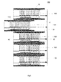
- Fig. 6 schematically shows a plot of a computational simulation of the electric field inside an exemplary modular electronic system according to conventional technology, having dielectric housings around the electronic circuits 110. Two modules are shown, wherein the electronic circuits 110 inside the housings are on the same test potential. It can be seen that the electric field lines exhibit a highly irregular spatial distribution, also in the space between the housings, indicating field peaks and leading to a significant risk of partial discharges.
- Fig. 7 schematically shows a simulation of the electric field inside a modular electronic system 150 according to embodiments.
- the electronic circuits 110 are on the same potential as the respective first or inner layers 40 of the modules 100.
- An electric field is located in this example between the grounded, outer layer or second layer 60, and the first layer or inner layer 40, which is on the same potential as circuit 110.
- the space between the two modules 100 is - in the shown example - free of an electric field, thus reducing the risk of partial discharges in the space outside the modules 100 to zero, respectively eliminating the probability of partial discharge.
- the field line distribuition is only shown in the dielectric enclosure wall 30; depending on the design of the electronic circuit 110, there may also be an electric field (not shown) between portions of the circuit 110 and the inner layer 40.
Landscapes
- Engineering & Computer Science (AREA)
- Microelectronics & Electronic Packaging (AREA)
- Casings For Electric Apparatus (AREA)
Priority Applications (2)
| Application Number | Priority Date | Filing Date | Title |
|---|---|---|---|
| EP12181155.8A EP2701477A1 (de) | 2012-08-21 | 2012-08-21 | Gehäuse für eine elektronische Vorrichtung |
| CN201320587564.0U CN203941898U (zh) | 2012-08-21 | 2013-08-21 | 用于电子装置的封装件、电子模块以及模块化电子系统 |
Applications Claiming Priority (1)
| Application Number | Priority Date | Filing Date | Title |
|---|---|---|---|
| EP12181155.8A EP2701477A1 (de) | 2012-08-21 | 2012-08-21 | Gehäuse für eine elektronische Vorrichtung |
Publications (1)
| Publication Number | Publication Date |
|---|---|
| EP2701477A1 true EP2701477A1 (de) | 2014-02-26 |
Family
ID=47071075
Family Applications (1)
| Application Number | Title | Priority Date | Filing Date |
|---|---|---|---|
| EP12181155.8A Withdrawn EP2701477A1 (de) | 2012-08-21 | 2012-08-21 | Gehäuse für eine elektronische Vorrichtung |
Country Status (2)
| Country | Link |
|---|---|
| EP (1) | EP2701477A1 (de) |
| CN (1) | CN203941898U (de) |
Cited By (4)
| Publication number | Priority date | Publication date | Assignee | Title |
|---|---|---|---|---|
| WO2015132128A1 (en) * | 2014-03-05 | 2015-09-11 | Abb Technology Ag | Enclosure for power electronic components |
| WO2019222781A1 (de) * | 2018-05-25 | 2019-11-28 | Miba Energy Holding Gmbh | Leistungsbaugruppe mit tragendem kühlkörper |
| EP3627982A1 (de) * | 2018-09-18 | 2020-03-25 | Delta Electronics, Inc. | Isoliertes gehäuse |
| EP4472051A4 (de) * | 2022-01-28 | 2026-04-01 | Ls Electric Co Ltd | Halbleitertransformator und modulare hochspannungsleistungsvorrichtung |
Families Citing this family (1)
| Publication number | Priority date | Publication date | Assignee | Title |
|---|---|---|---|---|
| FR3041209B1 (fr) * | 2015-09-15 | 2017-09-15 | Sagem Defense Securite | Systeme electronique compact et dispositif comprenant un tel systeme |
Citations (2)
| Publication number | Priority date | Publication date | Assignee | Title |
|---|---|---|---|---|
| US6163457A (en) * | 1998-09-09 | 2000-12-19 | Daimlerchrysler Ag | Module of a circuit arrangement which is preferably contained in a drive for a railroad vehicle and is of modular construction |
| US20100328883A1 (en) * | 2009-06-30 | 2010-12-30 | Enrique Ledezma | Pluggable Power Cell For An Inverter |
-
2012
- 2012-08-21 EP EP12181155.8A patent/EP2701477A1/de not_active Withdrawn
-
2013
- 2013-08-21 CN CN201320587564.0U patent/CN203941898U/zh not_active Expired - Lifetime
Patent Citations (2)
| Publication number | Priority date | Publication date | Assignee | Title |
|---|---|---|---|---|
| US6163457A (en) * | 1998-09-09 | 2000-12-19 | Daimlerchrysler Ag | Module of a circuit arrangement which is preferably contained in a drive for a railroad vehicle and is of modular construction |
| US20100328883A1 (en) * | 2009-06-30 | 2010-12-30 | Enrique Ledezma | Pluggable Power Cell For An Inverter |
Non-Patent Citations (2)
| Title |
|---|
| BERTH M.: "New Main Circuits, HV-Design of Submodules", ABB-REPORT, HIP49/ATP5-3 |
| STEINER M.; REINOLD, H.: "Medium Frequency Topology in Railway Applications", EUROPEAN RAILWAY REVIEW (EPE, 2007 |
Cited By (7)
| Publication number | Priority date | Publication date | Assignee | Title |
|---|---|---|---|---|
| WO2015132128A1 (en) * | 2014-03-05 | 2015-09-11 | Abb Technology Ag | Enclosure for power electronic components |
| WO2019222781A1 (de) * | 2018-05-25 | 2019-11-28 | Miba Energy Holding Gmbh | Leistungsbaugruppe mit tragendem kühlkörper |
| CN112237056A (zh) * | 2018-05-25 | 2021-01-15 | 米巴能源控股有限公司 | 具有承载式冷却体的功率组件 |
| US11337328B2 (en) | 2018-05-25 | 2022-05-17 | Miba Energy Holding Gmbh | Power assembly having a load-bearing cooling body |
| EP3627982A1 (de) * | 2018-09-18 | 2020-03-25 | Delta Electronics, Inc. | Isoliertes gehäuse |
| US10986745B2 (en) | 2018-09-18 | 2021-04-20 | Delta Electronics, Inc. | Insulated housing having a cylindrical structure |
| EP4472051A4 (de) * | 2022-01-28 | 2026-04-01 | Ls Electric Co Ltd | Halbleitertransformator und modulare hochspannungsleistungsvorrichtung |
Also Published As
| Publication number | Publication date |
|---|---|
| CN203941898U (zh) | 2014-11-12 |
Similar Documents
| Publication | Publication Date | Title |
|---|---|---|
| US9490555B1 (en) | System or connector for voltage bus structures | |
| CA2909962C (en) | Bus bar arrangement and a shroud for the same | |
| EP2701477A1 (de) | Gehäuse für eine elektronische Vorrichtung | |
| CN108123617B (zh) | 用于安装高低压转换电路的装置、高低压转换系统及电源 | |
| US7872843B2 (en) | Telecom power distribution unit with integrated filtering and telecom shelf cooling mechanisms | |
| CN105408170B (zh) | 具有连接器化隔离壁的高电压电气中心 | |
| JP6753399B2 (ja) | 端子接続構造およびこの構造を備えるサーバ用電源システム | |
| CN103582976A (zh) | 插入式复合配电组件和包括该组件的系统 | |
| KR102803024B1 (ko) | 배터리 시스템 내 커패시턴스 감소 | |
| AU2015249128B2 (en) | Electrical device | |
| EP2701476A1 (de) | Elektronisches Modul und modulares Elektroniksystem, das dieses verwendet | |
| CN201656757U (zh) | 多路输入/输出交直流电源与信号线滤波的滤波器 | |
| CN105023747A (zh) | 用于减小电容器的电端子上的机械载荷的方法和装置 | |
| CN104953802A (zh) | 电磁兼容滤波器 | |
| EP3114913B1 (de) | Gehäuse für leistungselektronische bauelemente | |
| CN104104223B (zh) | Dc-dc模块电源机架结构 | |
| WO2015088598A1 (en) | Switchgear module | |
| CN104380548A (zh) | 用于插入电路断路器控制板的电路断路器转接器 | |
| CN215580007U (zh) | 一种具有散热孔防尘功能的中置式开关柜 | |
| CN204290058U (zh) | 触头盒、安装组件和开关设备 | |
| JP6308453B2 (ja) | 電力変換装置 | |
| CN110729682A (zh) | 电气安装保护箱及电气接线装置 | |
| CN116760380A (zh) | 一种基于叠层母排的滤波装置 | |
| EP3066906B1 (de) | Stromverteilungsanordnung und kopfanordnung dafür | |
| DE202013007399U1 (de) | Gehäuse für eine Elektronikeinrichtung |
Legal Events
| Date | Code | Title | Description |
|---|---|---|---|
| PUAI | Public reference made under article 153(3) epc to a published international application that has entered the european phase |
Free format text: ORIGINAL CODE: 0009012 |
|
| AK | Designated contracting states |
Kind code of ref document: A1 Designated state(s): AL AT BE BG CH CY CZ DE DK EE ES FI FR GB GR HR HU IE IS IT LI LT LU LV MC MK MT NL NO PL PT RO RS SE SI SK SM TR |
|
| AX | Request for extension of the european patent |
Extension state: BA ME |
|
| STAA | Information on the status of an ep patent application or granted ep patent |
Free format text: STATUS: THE APPLICATION IS DEEMED TO BE WITHDRAWN |
|
| 18D | Application deemed to be withdrawn |
Effective date: 20140827 |