EP2703876A1 - Réseau de cristaux liquides tactile, dispositif d'affichage tactile 3D et procédé de commande d'un réseau de cristaux liquides tactile - Google Patents
Réseau de cristaux liquides tactile, dispositif d'affichage tactile 3D et procédé de commande d'un réseau de cristaux liquides tactile Download PDFInfo
- Publication number
- EP2703876A1 EP2703876A1 EP13182402.1A EP13182402A EP2703876A1 EP 2703876 A1 EP2703876 A1 EP 2703876A1 EP 13182402 A EP13182402 A EP 13182402A EP 2703876 A1 EP2703876 A1 EP 2703876A1
- Authority
- EP
- European Patent Office
- Prior art keywords
- liquid crystal
- electrodes
- grating
- touch
- substrate
- Prior art date
- Legal status (The legal status is an assumption and is not a legal conclusion. Google has not performed a legal analysis and makes no representation as to the accuracy of the status listed.)
- Granted
Links
Images




Classifications
-
- G—PHYSICS
- G02—OPTICS
- G02F—OPTICAL DEVICES OR ARRANGEMENTS FOR THE CONTROL OF LIGHT BY MODIFICATION OF THE OPTICAL PROPERTIES OF THE MEDIA OF THE ELEMENTS INVOLVED THEREIN; NON-LINEAR OPTICS; FREQUENCY-CHANGING OF LIGHT; OPTICAL LOGIC ELEMENTS; OPTICAL ANALOGUE/DIGITAL CONVERTERS
- G02F1/00—Devices or arrangements for the control of the intensity, colour, phase, polarisation or direction of light arriving from an independent light source, e.g. switching, gating or modulating; Non-linear optics
- G02F1/01—Devices or arrangements for the control of the intensity, colour, phase, polarisation or direction of light arriving from an independent light source, e.g. switching, gating or modulating; Non-linear optics for the control of the intensity, phase, polarisation or colour
- G02F1/13—Devices or arrangements for the control of the intensity, colour, phase, polarisation or direction of light arriving from an independent light source, e.g. switching, gating or modulating; Non-linear optics for the control of the intensity, phase, polarisation or colour based on liquid crystals, e.g. single liquid crystal display cells
- G02F1/1313—Devices or arrangements for the control of the intensity, colour, phase, polarisation or direction of light arriving from an independent light source, e.g. switching, gating or modulating; Non-linear optics for the control of the intensity, phase, polarisation or colour based on liquid crystals, e.g. single liquid crystal display cells specially adapted for a particular application
-
- G—PHYSICS
- G02—OPTICS
- G02B—OPTICAL ELEMENTS, SYSTEMS OR APPARATUS
- G02B30/00—Optical systems or apparatus for producing three-dimensional [3D] effects, e.g. stereoscopic images
- G02B30/20—Optical systems or apparatus for producing three-dimensional [3D] effects, e.g. stereoscopic images by providing first and second parallax images to an observer's left and right eyes
- G02B30/26—Optical systems or apparatus for producing three-dimensional [3D] effects, e.g. stereoscopic images by providing first and second parallax images to an observer's left and right eyes of the autostereoscopic type
- G02B30/27—Optical systems or apparatus for producing three-dimensional [3D] effects, e.g. stereoscopic images by providing first and second parallax images to an observer's left and right eyes of the autostereoscopic type involving lenticular arrays
-
- G—PHYSICS
- G02—OPTICS
- G02B—OPTICAL ELEMENTS, SYSTEMS OR APPARATUS
- G02B30/00—Optical systems or apparatus for producing three-dimensional [3D] effects, e.g. stereoscopic images
- G02B30/20—Optical systems or apparatus for producing three-dimensional [3D] effects, e.g. stereoscopic images by providing first and second parallax images to an observer's left and right eyes
- G02B30/26—Optical systems or apparatus for producing three-dimensional [3D] effects, e.g. stereoscopic images by providing first and second parallax images to an observer's left and right eyes of the autostereoscopic type
- G02B30/30—Optical systems or apparatus for producing three-dimensional [3D] effects, e.g. stereoscopic images by providing first and second parallax images to an observer's left and right eyes of the autostereoscopic type involving parallax barriers
-
- G—PHYSICS
- G02—OPTICS
- G02F—OPTICAL DEVICES OR ARRANGEMENTS FOR THE CONTROL OF LIGHT BY MODIFICATION OF THE OPTICAL PROPERTIES OF THE MEDIA OF THE ELEMENTS INVOLVED THEREIN; NON-LINEAR OPTICS; FREQUENCY-CHANGING OF LIGHT; OPTICAL LOGIC ELEMENTS; OPTICAL ANALOGUE/DIGITAL CONVERTERS
- G02F1/00—Devices or arrangements for the control of the intensity, colour, phase, polarisation or direction of light arriving from an independent light source, e.g. switching, gating or modulating; Non-linear optics
- G02F1/01—Devices or arrangements for the control of the intensity, colour, phase, polarisation or direction of light arriving from an independent light source, e.g. switching, gating or modulating; Non-linear optics for the control of the intensity, phase, polarisation or colour
- G02F1/13—Devices or arrangements for the control of the intensity, colour, phase, polarisation or direction of light arriving from an independent light source, e.g. switching, gating or modulating; Non-linear optics for the control of the intensity, phase, polarisation or colour based on liquid crystals, e.g. single liquid crystal display cells
- G02F1/133—Constructional arrangements; Operation of liquid crystal cells; Circuit arrangements
- G02F1/1333—Constructional arrangements; Manufacturing methods
- G02F1/13338—Input devices, e.g. touch panels
-
- G—PHYSICS
- G06—COMPUTING OR CALCULATING; COUNTING
- G06F—ELECTRIC DIGITAL DATA PROCESSING
- G06F3/00—Input arrangements for transferring data to be processed into a form capable of being handled by the computer; Output arrangements for transferring data from processing unit to output unit, e.g. interface arrangements
- G06F3/01—Input arrangements or combined input and output arrangements for interaction between user and computer
- G06F3/03—Arrangements for converting the position or the displacement of a member into a coded form
- G06F3/041—Digitisers, e.g. for touch screens or touch pads, characterised by the transducing means
- G06F3/0412—Digitisers structurally integrated in a display
-
- G—PHYSICS
- G06—COMPUTING OR CALCULATING; COUNTING
- G06F—ELECTRIC DIGITAL DATA PROCESSING
- G06F3/00—Input arrangements for transferring data to be processed into a form capable of being handled by the computer; Output arrangements for transferring data from processing unit to output unit, e.g. interface arrangements
- G06F3/01—Input arrangements or combined input and output arrangements for interaction between user and computer
- G06F3/03—Arrangements for converting the position or the displacement of a member into a coded form
- G06F3/041—Digitisers, e.g. for touch screens or touch pads, characterised by the transducing means
- G06F3/044—Digitisers, e.g. for touch screens or touch pads, characterised by the transducing means by capacitive means
- G06F3/0445—Digitisers, e.g. for touch screens or touch pads, characterised by the transducing means by capacitive means using two or more layers of sensing electrodes, e.g. using two layers of electrodes separated by a dielectric layer
-
- G—PHYSICS
- G06—COMPUTING OR CALCULATING; COUNTING
- G06F—ELECTRIC DIGITAL DATA PROCESSING
- G06F3/00—Input arrangements for transferring data to be processed into a form capable of being handled by the computer; Output arrangements for transferring data from processing unit to output unit, e.g. interface arrangements
- G06F3/01—Input arrangements or combined input and output arrangements for interaction between user and computer
- G06F3/03—Arrangements for converting the position or the displacement of a member into a coded form
- G06F3/041—Digitisers, e.g. for touch screens or touch pads, characterised by the transducing means
- G06F3/044—Digitisers, e.g. for touch screens or touch pads, characterised by the transducing means by capacitive means
- G06F3/0446—Digitisers, e.g. for touch screens or touch pads, characterised by the transducing means by capacitive means using a grid-like structure of electrodes in at least two directions, e.g. using row and column electrodes
-
- H—ELECTRICITY
- H04—ELECTRIC COMMUNICATION TECHNIQUE
- H04N—PICTORIAL COMMUNICATION, e.g. TELEVISION
- H04N13/00—Stereoscopic video systems; Multi-view video systems; Details thereof
- H04N13/30—Image reproducers
- H04N13/302—Image reproducers for viewing without the aid of special glasses, i.e. using autostereoscopic displays
- H04N13/31—Image reproducers for viewing without the aid of special glasses, i.e. using autostereoscopic displays using parallax barriers
-
- G—PHYSICS
- G02—OPTICS
- G02F—OPTICAL DEVICES OR ARRANGEMENTS FOR THE CONTROL OF LIGHT BY MODIFICATION OF THE OPTICAL PROPERTIES OF THE MEDIA OF THE ELEMENTS INVOLVED THEREIN; NON-LINEAR OPTICS; FREQUENCY-CHANGING OF LIGHT; OPTICAL LOGIC ELEMENTS; OPTICAL ANALOGUE/DIGITAL CONVERTERS
- G02F1/00—Devices or arrangements for the control of the intensity, colour, phase, polarisation or direction of light arriving from an independent light source, e.g. switching, gating or modulating; Non-linear optics
- G02F1/01—Devices or arrangements for the control of the intensity, colour, phase, polarisation or direction of light arriving from an independent light source, e.g. switching, gating or modulating; Non-linear optics for the control of the intensity, phase, polarisation or colour
- G02F1/13—Devices or arrangements for the control of the intensity, colour, phase, polarisation or direction of light arriving from an independent light source, e.g. switching, gating or modulating; Non-linear optics for the control of the intensity, phase, polarisation or colour based on liquid crystals, e.g. single liquid crystal display cells
- G02F1/133—Constructional arrangements; Operation of liquid crystal cells; Circuit arrangements
- G02F1/1333—Constructional arrangements; Manufacturing methods
- G02F1/1343—Electrodes
- G02F1/134309—Electrodes characterised by their geometrical arrangement
- G02F1/134363—Electrodes characterised by their geometrical arrangement for applying an electric field parallel to the substrate, i.e. in-plane switching [IPS]
Definitions
- Embodiments of the present invention relate to a touch liquid crystal grating, a 3D touch display device and a driving method of the touch liquid crystal grating.
- the 3D (three-dimensional) display technology has attracted a lot of attentions, and its most fundamental principle is: different pictures are received by left and right eyes of a person, respectively, and then are subjected to superimposing, renascence of image information, etc., in a brain, thereby forming a stereoscopic image.
- a common liquid crystal grating generally comprises an upper polarizer, a lower polarizer, an upper substrate, a lower substrate and a liquid crystal layer between the two substrates, and strip-like electrodes and a plane electrode are provided on the upper substrate and the lower substrate, respectively.
- Its specific operation principle is as follows: when the liquid crystal grating is electrified, liquid crystal molecules corresponding to the strip-like electrodes are deflected, and other liquid crystal molecules remain the same.
- a polarized light parallel to an absorption axis of the lower polarizer enters the liquid crystal layer will change its vibration direction upon passing through the liquid crystal molecules that remain the same without deflection, and its vibration direction is just parallel to an absorption axis of the upper polarizer when it reaches the upper polarizer, so that the light pass through; while passing through the liquid crystal molecules that are deflected, the polarized light will not change the vibration direction, and its vibration direction is perpendicular to the absorption axis of the upper polarizer when it reaches the upper polarizer, so that the light is blocked.
- a parallax barrier perpendicular to an extending direction of strip-like electrodes is formed, thereby achieving the three-dimensional grating display mode.
- a right eye will be sheltered from it by opaque stripes
- the left eye will be sheltered from it by opaque stripes.
- the liquid crystal grating having a touch function has at least four layers of electrode, and a large number of electrode layers will reduce the transmittance of the whole liquid crystal grating.
- a conductive adhesive needs to be used for conduction of a voltage signal, and alignment marks also need to be provided on the two substrate, respectively, so as to be precisely cell-assembled for use, which increases the fabrication cost as well.
- Embodiments of the invention provide a touch liquid crystal grating, a 3D touch display device and a driving method of the touch liquid crystal grating, by which, a touch liquid crystal grating with a high light transmittance and a low fabrication cost is achieved.
- a touch liquid crystal grating comprising: a first substrate; a second substrate, cell-assembled with the first substrate; and a liquid crystal layer, filled between the first substrate and the second substrate; a plurality of grating electrodes, which are located on a side of the first substrate that faces the liquid crystal layer and extend along a first direction, each of the plurality of grating electrodes being located within each of strip-like regions with spacing regions being provided therebetween; a plurality of touch driving electrodes, which extend along the first direction and are located on the side of the first substrate facing the liquid crystal layer, the touch driving electrodes being located within the spacing regions between adjacent strip-like regions; and a plurality of touch sensing electrodes, which extend along a second direction and are located on a side of the first substrate opposed to the liquid crystal layer, wherein the first direction is different from the second direction, and in a condition that the plurality of grating electrodes are electrified, liquid crystal molecules corresponding to each of the strip-like regions
- a 3D display device comprising: a display device; and a touch liquid crystal grating, disposed at a light exiting side of the display device, the touch liquid crystal grating being the touch liquid crystal grating as stated above.
- a driving method of the touch liquid crystal grating comprising: in a condition that the touch liquid crystal grating is in a 3D display mode, for each of grating electrodes, its grating sub-electrodes in odd-numbered rows are applied with a first voltage, and its grating sub-electrodes in even-numbered rows are applied with a second voltage, wherein the first voltage is not equal to the second voltage so that liquid crystal molecules corresponding to each of the grating electrodes are deflected, while each of the touch driving electrodes is applied with the first voltage or the second voltage as one or both of adjacent grating sub-electrodes, and the touch sensing electrodes are applied with a voltage different from that applied to the touch driving electrodes; in a condition that the touch liquid crystal grating is in a 2D display mode, the grating electrodes and the touch driving electrodes of the touch liquid crystal grating are grounded or applied with the same voltage, and the touch sensing
- FIG. 1 is a structurally schematic view illustrating a liquid crystal grating in prior art
- FIG. 2 is a structurally schematic view illustrating a touch liquid crystal grating provided by an embodiment of the invention
- FIG. 3 is a schematic view illustrating strip-like regions and spacing regions of the touch liquid crystal grating provided by an embodiment of the invention
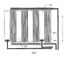
- FIG. 4 is a top view illustrating a side of a first substrate facing a liquid crystal layer, provided by an embodiment of the invention
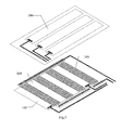
- FIG. 5 is a schematically, structurally exploded view illustrating two sides of a first substrate provided by an embodiment of the invention
- FIG. 6 is a schematic view illustrating a principle of touch and 3D display functions provided by an embodiment of the invention.
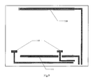
- FIG. 7 to FIG. 9 are schematic views illustrating various steps upon manufacture of the side of the first substrate that faces the liquid crystal layer, provided by an embodiment of the invention.
- An embodiment of the invention provides a touch liquid crystal grating 1. As shown in FIG. 2 , it comprises: a first substrate 101; a second substrate 102, cell-assembled with the first substrate 101; a liquid crystal layer 103, filled between the first substrate 101 and the second substrate 102; a plurality of grating electrodes 104, which are located on a side of the first substrate 101 that faces the liquid crystal layer 103 and extend along a first direction, each of the plurality of grating electrodes 104 being disposed within each of strip-like regions A; a plurality of touch driving electrodes 105, which extend along the first direction and are located on the side of the first substrate 101 that faces the liquid crystal layer 103, each of the plurality of touch driving electrodes 105 being disposed with a spacing region B between adjacent strip-like regions A; and a touch sensing electrode 106, which extends along a second direction and is located on a side of the first substrate 101 opposed to the liquid crystal layer 103, wherein the first direction is different from the second direction,
- liquid crystal molecules corresponding to the plurality of strip-like regions A are deflected, while liquid crystal molecules corresponding to the spacing regions B are not deflected.
- each of the grating electrodes 104 comprises two or more strip-like grating sub-electrodes 1041 that are disposed parallel to each other, and adjacent strip-like grating sub-electrodes 1041 are applied with different voltages so that there is a voltage difference between them.
- the same ones of ends of grating sub-electrodes in odd-numbered rows may be connected together through a wire, and the same ones of ends of grating sub-electrodes in even-numbered rows may be connected together through a wire; alternatively, ones of ends of grating sub-electrodes in odd-numbered rows are connected to a common, external lead terminal through leads, respectively, and ones of ends of grating sub-electrodes in even-numbered rows are connected to a common, external lead terminal through leads, respectively.
- the same ones of ends of grating sub-electrodes in odd-numbered rows for different grating electrodes are connected together, and grating sub-electrodes in even-numbered rows for different grating electrodes are connected together; or, ones of ends of grating sub-electrodes in odd-numbered rows for different grating electrodes are connected to a common, external lead terminal through leads, respectively, and ones of ends of grating sub-electrodes in even-numbered rows are connected to a common, external lead terminal through leads, respectively; or, within each of grating electrodes, ones of ends of grating sub-electrodes in odd-numbered rows are connected together, and ones of ends of grating sub-electrodes in even-numbered rows are connected together, and for different grating electrodes, their grating sub-electrodes are individually connected to external lead terminals through respective leads.
- an ITO (Indium Tin Oxide) material may be used for formation of the grating electrodes 104, the touch driving electrodes 105 and the touch sensing electrodes 106.
- the touch liquid crystal grating 1 in the embodiment further comprises: a first polarizer 107 located on a side of the touch sensing electrode 106 opposed to the liquid crystal layer 103, and a second polarizer 108 located on a side of the second substrate 102 opposed to the liquid crystal layer 103, directions of transmission axes of the first polarizer 107 and the second polarizer 108 are parallel.
- Liquid crystal molecules in the liquid crystal layer 103 are aligned in parallel along the direction of the transmission axis of the first polarizer when no power is applied to them.
- directions of transmission axes of the first polarizer 107 and the second polarizer 108 are arranged to be parallel to each other, and in the event that no power is applied to grating electrodes 104 of the liquid crystal grating, liquid crystal molecules have no delay function on polarized light that pass through it after being transmitted by the second polarizer 108, so that the polarized light passing through the liquid crystal molecules has a polarization direction along the direction of transmission axis of the first polarizer 107. Therefore, a bright field is formed at each of the strip-like regions A and each of the spacer regions B, i.e., the entire touch liquid crystal grating 1 is pervious to light.
- liquid crystal molecules corresponding to the strip-like regions A are deflected to have a delay function on the polarized light that pass through it after being transmitted by the second polarizer 108. Accordingly, the polarized light passing through the liquid crystal molecules have a polarization direction different from the direction of transmission axis of the first polarizer 107 and can not pass through the first polarizer 107, thereby forming a dark field at the strip-like regions A.
- liquid crystal molecules at the spacing regions B are not deflected, so as to form a bright field.
- the entire touch liquid crystal grating 1 is formed as a grating with alternately bright and dark stripes. As regards the touch liquid crystal grating in the embodiment, by means of controlling a voltage applied to the grating electrodes 104, free conversion between the 2D and 3D displays can be realized.
- the touch liquid crystal grating provided by the embodiment of the invention when applied to a liquid crystal display device, it is possible that two layers of polarizers at a contact face of the liquid crystal display device and the touch liquid crystal grating as well as the second substrate 102 of the touch liquid crystal grating are omitted, and the first substrate 101 of the touch liquid crystal grating is directly cell-assembled with a color filter substrate of the liquid crystal panel.
- a function of 3D touch display can also be realized. Its principle is similar to that in the example provided by the embodiment of the invention, and details are omitted here.
- the touch liquid crystal grating provided by the embodiment of the invention is applied to a liquid crystal panel, it is possible that only one layer of polarizer is provided at a contact face of the liquid crystal panel and the touch liquid crystal grating, and the direction of transmission axis of the polarizer is parallel to the direction of transmission axis of the polarizer 107 over the first substrate 101, but is parallel to or perpendicular to the direction of transmission axis of a polarizer provided on an array substrate of the liquid crystal panel.
- a width a of the strip-like regions A of the touch liquid crystal grating and a width b of the spacing regions B between adjacent strip-like regions A are the same, and moreover, the width a of the strip-like regions A disposed on the touch liquid crystal grating should be half of the width of a sub-pixel of the display device.
- the width of the strip-like regions and the width of the spacing regions may be determined according to actual circumstances, as long as alternately bright and dark stripes can be formed to realize the 3D display.
- the relationship between the widths of the strip-like regions and the spacing regions and the width of a sub-pixel unit may also be determined according to actual requirements, as long as the 3D display can be realized.
- a grating electrode 104 in the touch liquid crystal grating provided by the embodiment of the invention includes at least two grating sub-electrodes 1041 that are parallel to each other.
- each of grating electrodes 104 includes seven grating sub-electrodes 1041, a extending direction of which is the same as the alignment direction (an arrow direction shown in FIG. 4 ) of liquid crystal molecules without electrified.
- each of grating electrodes 104 the any same ones of ends of grating sub-electrodes 1041 in odd-numbered rows (represented by grating sub-electrodes 1041 with inclined lines in FIG. 4 ) are connected together through a wire or electrode in the same layer, and the any same ones of ends of grating sub-electrodes 1041 in even-numbered rows (represented by hollowed grating sub-electrodes 1041 in FIG. 4 ) are connected together through an electrode or an wire in the same layer.
- a pattern size of a touch electrode is usually in the millimeter level, while a width between barriers for three-dimensional display is usually in the micron level.
- electrodes necessary for a touch screen are much smaller in number than electrodes necessary for a parallax barrier. Therefore, in the touch liquid crystal grating, the number of touch electrodes is also far smaller than the number of grating electrodes for 3D display. As such, as shown in FIG.
- touch driving electrodes 105 may be provided within a part of the spacing regions B, and in order to adjust the optical matching of the touch liquid crystal grating, Dummy electrodes 109 may be provided within other spacing regions B except those within which the touch driving electrodes 105 have been provided, and the Dummy electrodes 109 are not necessary to be applied with any voltage.
- provision of the Dummy electrodes 109 can also raise the Signal to Noise Ratio (SNR) between the touch driving electrodes 105 and the touch sensing electrodes 106, and improve the sensitivity of the touch.
- SNR Signal to Noise Ratio
- the grating electrodes 104, the touch driving electrodes 105 and the Dummy electrodes 109 may be disposed in the same layer, namely, they are fabricated in one patterning process, and this can decrease the number of layers in the touch liquid crystal grating, thereby increasing its transmittance.
- each of the Dummy electrodes 109 may be composed of at least two strip-like sub-electrodes that are parallel to each other.
- the arranged density of strip-like sub-electrodes may conform to the arranged density of grating sub-electrodes 1041 in a grating electrode 104.
- each of the touch driving electrodes 105 may be composed of at least two touch driving sub-electrodes that are parallel to each other as well, and any ones of ends of the touch driving sub-electrodes constituting one touch driving electrode get conduction through a wire.
- the arranged density of the touch driving sub-electrodes may conform to the arranged density of the grating sub-electrodes 1041 in a grating electrode 104, so as to achieve maximization of optical matching.
- double-layered touch electrodes are employed, namely, the touch driving electrodes 105 and the touch sensing electrodes 106 are disposed in two layers, and the first substrate 101 interposed between them serves as an insulating layer.
- a relationship of being non-uniplanar and perpendicular will be usually formed between a touch sensing electrode 106 and a touch driving electrode 105, and a sensing capacitor is formed at the non-uniplanar intersection of the two electrodes.
- the working process of it is: when a touch driving signal is applied to the touch driving electrode, a voltage signal generated on the touch sensing electrode by coupling of the sensing capacitor is detected; in this course, in a case that a human body contacts with the touch screen, an electric field of the human body will act on the sensing capacitor so that a capacitance of the sensing capacitor is changed, and thus the voltage signal generated on the touch sensing electrode by coupling is changed; in accordance with the change of the voltage signal, a contact position can be determined.
- a touch signal and a grating display signal will interfere with each other, while in the touch liquid crystal grating provided by the embodiment of the invention, liquid crystal molecules directly under the touch driving electrodes 105 for transmitting the touch signal will not be deflected so that a interference will not occur between the touch signal and the grating display signal.
- the touch sensing electrodes 106 for sensing the touch signal are located above the first substrate, and the first substrate 101 functions as an insulating layer between the touch driving electrodes 105 and the touch sensing electrodes 106.
- the first substrate 101 is usually a glass substrate, which is generally thicker so that a distance between the touch sensing electrode 106 and the grating electrode 104 can be increased. This allows a capacitance Csp produced between the two to make a minimal impact on liquid crystal molecules disposed under the grating electrode 104, or even to make no impact on a deflection direction of liquid crystal molecules essentially. Therefore, the 3D display and touch functions can be better achieved by the touch liquid crystal grating provided by the embodiment of the invention simultaneously.
- a manufacture process of one side of its upper substrate 101 that faces the liquid crystal layer 103 may comprise several steps as follows:
- grating electrodes 104, touch driving electrodes 105 and Dummy electrodes 109 are fabricated on the first substrate 101 through one patterning process, as shown in FIG. 7 .
- the via hole specifically comprises a via hole 110 through which grating sub-electrodes 1041 in odd-numbered rows get conduction, a via hole 111 through which grating sub-electrodes 1041 in even-numbered rows get conduction, and a via hole 112 through which the touch driving electrodes 105 get conduction.
- a metal wiring is formed on the insulating layer, as shown in FIG. 9 .
- the resistance of the metal wiring is far lower than the resistance of an ITO electrode, in addition to the function of conduction, the metal wiring positioned in the via hole 110 through which the grating sub-electrodes 1041 in odd-numbered rows get conduction and the via hole 111 through which the grating sub-electrodes 1041 in even-numbered rows get conduction can also play a function of reducing a resistance of the grating sub-electrodes 1041.
- the voltage loss is reduced.
- a manufacture process of one side of the upper substrate 101 that is opposed to the liquid crystal layer 103 may comprise three steps of fabricating a metal wiring, fabricating touch sensing electrodes 106 and coating an insulating protection layer, and details are omitted here.
- a driving method of the above touch liquid crystal grating comprising:
- grating sub-electrodes in odd-numbered rows that are included in a grating electrode disposed in each of strip-like regions A are applied with a first voltage
- grating sub-electrodes in even-numbered rows that are included in it are applied with a second voltage, wherein the first voltage is not equal to the second voltage so that liquid crystal molecules corresponding to each grating electrode are deflected.
- each of touch driving electrodes is applied with the first voltage or the second voltage as one or both of adjacent grating sub-electrodes
- each of touch sensing electrodes is applied with a voltage different from the first voltage and the second voltage.
- the grating electrodes and the touch driving electrodes of the touch liquid crystal grating are grounded or applied with the same voltage so that liquid crystal molecules corresponding to the grating electrodes are not deflected, and the touch sensing electrodes are applied with a voltage different from that applied to the touch driving electrodes, so as to realize the touch function.
- applying the same voltage to grating electrodes of the touch liquid crystal grating means that the same voltage is applied to grating sub-electrodes in odd-numbered rows and grating sub-electrodes in even-numbered rows of each grating electrode so as not to produce a voltage difference between the two.
- an embodiment of the invention further provides a 3D touch display device, comprising a display device and a liquid crystal grating disposed on a light exiting face of the display device, the liquid crystal grating being the above touch liquid crystal grating provided by the embodiment of the invention.
- the display device may be a liquid crystal display device (LCD), an organic electroluminescent display device (OLED), a plasma display device (PDP), a cathode ray display device (CRT), or the like.
- LCD liquid crystal display device
- OLED organic electroluminescent display device
- PDP plasma display device
- CRT cathode ray display device
- the display device is a liquid crystal display device, wherein the TFT array substrate and an opposite substrate are disposed to face each other to form a liquid crystal cell, and a liquid crystal material is filled in the liquid crystal cell.
- the opposite substrate is a color filter substrate, for example.
- a pixel electrode of each pixel unit of the TFT array substrate is used to apply an electric field, so as to control a rotation of the liquid crystal material and to perform a displaying operation.
- the liquid crystal display device further comprises a backlight source provided for the display device.
- OLED organic light emitting display
- grating electrodes are provided within strip-like regions on a side of the first substrate facing the liquid crystal layer and with spacing regions provided between each other, and a grating electrode within each of the strip-like regions comprises a plurality of strip-like grating sub-electrodes, with touch driving electrodes being provided within spacing regions between adjacent strip-like regions; on a side of the first substrate opposed to the liquid crystal layer are provided touch sensing electrodes having different extending direction from the touch driving electrodes; when power is applied to a grating electrode, an electric field can be generated to make corresponding liquid crystal molecules be deflected, so that a strip-like grating is formed, and a touch function can be realized with the use of the touch driving electrodes and touch sensing electrodes that are insulated by the first substrate.
- the strip-like grating can be formed merely by forming a layer of grating electrodes on the first substrate, the number of electrode layer is decreased, and the transmittance of the whole liquid crystal grating is enhanced; furthermore, because both the touch electrodes and the grating electrodes are provided on the first substrate, it is unnecessary to use a conductive adhesive for conduction of a voltage signal, and to arrange an alignment mark on the second substrate as well, whereby the fabrication process is simplified, and the production cost is saved.
Landscapes
- Engineering & Computer Science (AREA)
- Physics & Mathematics (AREA)
- General Physics & Mathematics (AREA)
- General Engineering & Computer Science (AREA)
- Theoretical Computer Science (AREA)
- Nonlinear Science (AREA)
- Optics & Photonics (AREA)
- Human Computer Interaction (AREA)
- Crystallography & Structural Chemistry (AREA)
- Chemical & Material Sciences (AREA)
- Mathematical Physics (AREA)
- Signal Processing (AREA)
- Multimedia (AREA)
- Liquid Crystal (AREA)
- Position Input By Displaying (AREA)
Applications Claiming Priority (1)
| Application Number | Priority Date | Filing Date | Title |
|---|---|---|---|
| CN201210320605.XA CN102830555B (zh) | 2012-08-31 | 2012-08-31 | 一种触控液晶光栅及3d触控显示装置 |
Publications (2)
| Publication Number | Publication Date |
|---|---|
| EP2703876A1 true EP2703876A1 (fr) | 2014-03-05 |
| EP2703876B1 EP2703876B1 (fr) | 2015-10-14 |
Family
ID=47333738
Family Applications (1)
| Application Number | Title | Priority Date | Filing Date |
|---|---|---|---|
| EP13182402.1A Active EP2703876B1 (fr) | 2012-08-31 | 2013-08-30 | Réseau de cristaux liquides tactile, dispositif d'affichage tactile 3D et procédé de commande d'un réseau de cristaux liquides tactile |
Country Status (3)
| Country | Link |
|---|---|
| US (1) | US9195081B2 (fr) |
| EP (1) | EP2703876B1 (fr) |
| CN (1) | CN102830555B (fr) |
Cited By (4)
| Publication number | Priority date | Publication date | Assignee | Title |
|---|---|---|---|---|
| EP3086209A1 (fr) * | 2015-04-24 | 2016-10-26 | Apple Inc. | Pixels flottants fusionnés dans un écran tactile |
| CN107870459A (zh) * | 2016-09-27 | 2018-04-03 | 褚建芬 | 3d触摸显示装置 |
| EP3200013A4 (fr) * | 2014-09-28 | 2018-05-02 | Boe Technology Group Co. Ltd. | Dispositif d'affichage tactile 3d, procédé de fabrication de ce dispositif, et procédé de pilotage associé |
| EP3282348A4 (fr) * | 2015-04-09 | 2018-11-21 | Boe Technology Group Co. Ltd. | Dispositif d'affichage tactile 3d à l' il nu doté d'un réseau, et ses procédés de fabrication et de commande |
Families Citing this family (31)
| Publication number | Priority date | Publication date | Assignee | Title |
|---|---|---|---|---|
| US9645431B2 (en) * | 2008-03-19 | 2017-05-09 | Egalax_Empia Technology Inc. | Touch display and method for driving a plurality of touch driving electrodes of touch display |
| CN103091909B (zh) * | 2013-01-29 | 2015-10-14 | 北京京东方光电科技有限公司 | 一种触控3d显示模组及其制作方法和触控3d显示装置 |
| CN104049814A (zh) * | 2013-03-13 | 2014-09-17 | 北京京东方光电科技有限公司 | 一种触控模组及其制造方法 |
| CN103309094B (zh) * | 2013-03-29 | 2016-01-06 | 北京京东方光电科技有限公司 | 一种液晶光栅、3d触控显示装置及液晶光栅的驱动方法 |
| CN103440067B (zh) | 2013-08-07 | 2016-06-29 | 北京京东方光电科技有限公司 | 一种显示面板、制备方法及显示装置 |
| CN104575371B (zh) * | 2013-10-24 | 2017-04-19 | 昆山工研院新型平板显示技术中心有限公司 | 一种触控3d显示面板及其控制方法 |
| US9569047B2 (en) | 2013-12-31 | 2017-02-14 | Boe Technology Group Co., Ltd. | Display device and method for preparing the same |
| CN103698926B (zh) * | 2013-12-31 | 2016-04-27 | 京东方科技集团股份有限公司 | 一种显示装置及其制备方法 |
| CN105094392A (zh) * | 2014-04-29 | 2015-11-25 | 宸鸿科技(厦门)有限公司 | 触控显示面板 |
| CN104123036B (zh) * | 2014-06-09 | 2017-02-01 | 京东方科技集团股份有限公司 | 光栅基板及其制作方法、显示装置 |
| CN104460136B (zh) * | 2014-12-30 | 2017-06-23 | 京东方科技集团股份有限公司 | 液晶光栅及其制作方法和驱动方法、拼接屏 |
| CN104536620A (zh) * | 2015-01-26 | 2015-04-22 | 京东方科技集团股份有限公司 | 触摸显示面板和触摸显示装置 |
| CN104699360B (zh) * | 2015-03-30 | 2018-04-27 | 京东方科技集团股份有限公司 | 一种电磁触控式三维光栅及显示装置 |
| CN104849886B (zh) * | 2015-06-09 | 2018-06-05 | 京东方科技集团股份有限公司 | 显示装置及其驱动方法、制作方法 |
| CN105093547B (zh) * | 2015-08-20 | 2019-06-07 | 京东方科技集团股份有限公司 | 3d显示装置及其驱动方法 |
| CN106708302A (zh) * | 2015-10-30 | 2017-05-24 | 京东方科技集团股份有限公司 | 一种压力检测装置、光栅、显示装置及其显示方法 |
| CN106959551B (zh) * | 2016-01-08 | 2023-12-19 | 京东方科技集团股份有限公司 | 一种显示装置及其驱动方法 |
| CN105467604B (zh) * | 2016-02-16 | 2018-01-12 | 京东方科技集团股份有限公司 | 一种3d显示装置及其驱动方法 |
| CN105549211A (zh) * | 2016-02-22 | 2016-05-04 | 京东方科技集团股份有限公司 | 3d触控显示模组及其控制方法和3d触控显示装置 |
| CN105867004B (zh) * | 2016-06-16 | 2019-11-08 | 上海天马微电子有限公司 | 触控光栅盒、触控光栅盒的驱动方法以及触控立体显示面板 |
| JP6736385B2 (ja) * | 2016-07-01 | 2020-08-05 | 株式会社ジャパンディスプレイ | 表示装置 |
| CN106125416A (zh) * | 2016-09-09 | 2016-11-16 | 万维云视(上海)数码科技有限公司 | 一种液晶光栅及其控制方法、3d显示面板及显示装置 |
| CN106200204B (zh) * | 2016-09-12 | 2023-09-22 | 合肥京东方光电科技有限公司 | 裸眼三维显示面板及其制造方法、裸眼三维显示装置 |
| CN106154657B (zh) * | 2016-09-12 | 2023-09-01 | 合肥鑫晟光电科技有限公司 | 一种3d显示装置及其制备方法 |
| CN107976854A (zh) * | 2016-10-21 | 2018-05-01 | 苏州今园科技创业孵化管理有限公司 | 液晶光栅的制作方法 |
| US10108285B1 (en) * | 2017-04-19 | 2018-10-23 | Superc-Touch Corporation | In-cell OLED touch display panel structure with high touch detection sensitivity and narrow border |
| CN109582162B (zh) * | 2017-09-28 | 2024-06-04 | 京东方科技集团股份有限公司 | 触控显示模组及其制作方法、触控显示装置 |
| WO2019200263A1 (fr) * | 2018-04-13 | 2019-10-17 | Tactual Labs Co. | Conducteurs couplés de manière capacitive |
| CN109062458B (zh) * | 2018-09-17 | 2021-05-28 | 昆山龙腾光电股份有限公司 | 触控显示面板及显示装置 |
| CN108920033B (zh) * | 2018-09-20 | 2021-12-28 | 合肥京东方光电科技有限公司 | 一种内嵌式触摸屏及显示装置 |
| CN116540455B (zh) | 2022-01-26 | 2026-04-17 | 合肥京东方光电科技有限公司 | 一种光栅调节装置、3d显示装置 |
Citations (1)
| Publication number | Priority date | Publication date | Assignee | Title |
|---|---|---|---|---|
| US20120105434A1 (en) * | 2010-10-28 | 2012-05-03 | Au Optronics Corporation | Switchable three-dimensional display |
Family Cites Families (16)
| Publication number | Priority date | Publication date | Assignee | Title |
|---|---|---|---|---|
| KR100728112B1 (ko) * | 2005-03-04 | 2007-06-13 | 삼성에스디아이 주식회사 | 배리어 장치, 이를 이용한 입체영상 표시장치 및 그의 구동방법 |
| JP2006343758A (ja) * | 2006-06-26 | 2006-12-21 | Mitsubishi Chemicals Corp | 反射防止方法及び反射防止構造並びに反射防止構造を有する反射防止構造体及びその製造方法 |
| US7952548B2 (en) * | 2007-03-09 | 2011-05-31 | Samsung Mobile Display Co., Ltd. | Electronic display device |
| KR101528143B1 (ko) * | 2007-11-02 | 2015-06-15 | 엘지디스플레이 주식회사 | 액정전계렌즈를 이용한 입체표시장치 |
| US8237677B2 (en) * | 2008-07-04 | 2012-08-07 | Tsinghua University | Liquid crystal display screen |
| TW201007520A (en) * | 2008-08-12 | 2010-02-16 | Univ Nat Chiao Tung | 3-dimensional interactive display and method for detecting 3-dimensional coordinates thereof |
| JP4816738B2 (ja) * | 2009-02-05 | 2011-11-16 | ソニー株式会社 | 情報入出力装置 |
| JP5484891B2 (ja) * | 2009-03-04 | 2014-05-07 | 株式会社ジャパンディスプレイ | 表示装置 |
| JP5191453B2 (ja) * | 2009-06-29 | 2013-05-08 | 株式会社ジャパンディスプレイウェスト | タッチセンサ、表示装置および電子機器 |
| US20110065480A1 (en) * | 2009-09-17 | 2011-03-17 | Chang Jae Kim | Mobile terminal |
| KR20110052241A (ko) * | 2009-11-12 | 2011-05-18 | 엘지디스플레이 주식회사 | 터치 패널 일체형 입체 영상 표시 장치 및 이의 제조 방법 |
| CN101957523B (zh) * | 2010-05-26 | 2013-01-09 | 天马微电子股份有限公司 | 液晶光栅模组及平面/立体可切换型液晶显示装置 |
| CN102645794B (zh) * | 2011-02-18 | 2015-01-28 | 群创光电股份有限公司 | 显示装置与液晶遮光面板 |
| KR101773613B1 (ko) * | 2011-02-25 | 2017-09-01 | 엘지디스플레이 주식회사 | 터치 일체형 표시장치 |
| CN102436101B (zh) * | 2011-12-26 | 2015-05-27 | 天马微电子股份有限公司 | 液晶透镜光栅和立体显示装置 |
| CN202837756U (zh) * | 2012-08-31 | 2013-03-27 | 北京京东方光电科技有限公司 | 一种触控液晶光栅及3d触控显示装置 |
-
2012
- 2012-08-31 CN CN201210320605.XA patent/CN102830555B/zh active Active
-
2013
- 2013-08-30 EP EP13182402.1A patent/EP2703876B1/fr active Active
- 2013-08-30 US US14/014,575 patent/US9195081B2/en active Active
Patent Citations (1)
| Publication number | Priority date | Publication date | Assignee | Title |
|---|---|---|---|---|
| US20120105434A1 (en) * | 2010-10-28 | 2012-05-03 | Au Optronics Corporation | Switchable three-dimensional display |
Cited By (9)
| Publication number | Priority date | Publication date | Assignee | Title |
|---|---|---|---|---|
| EP3200013A4 (fr) * | 2014-09-28 | 2018-05-02 | Boe Technology Group Co. Ltd. | Dispositif d'affichage tactile 3d, procédé de fabrication de ce dispositif, et procédé de pilotage associé |
| EP3282348A4 (fr) * | 2015-04-09 | 2018-11-21 | Boe Technology Group Co. Ltd. | Dispositif d'affichage tactile 3d à l' il nu doté d'un réseau, et ses procédés de fabrication et de commande |
| EP3086209A1 (fr) * | 2015-04-24 | 2016-10-26 | Apple Inc. | Pixels flottants fusionnés dans un écran tactile |
| CN106066728A (zh) * | 2015-04-24 | 2016-11-02 | 苹果公司 | 触摸屏中合并的悬浮像素 |
| US10353516B2 (en) | 2015-04-24 | 2019-07-16 | Apple Inc. | Merged floating pixels in a touch screen |
| CN106066728B (zh) * | 2015-04-24 | 2021-01-05 | 苹果公司 | 触摸屏中合并的悬浮像素 |
| CN112764578A (zh) * | 2015-04-24 | 2021-05-07 | 苹果公司 | 触摸屏中合并的悬浮像素 |
| US11893183B2 (en) | 2015-04-24 | 2024-02-06 | Apple Inc. | Merged floating pixels in a touch screen |
| CN107870459A (zh) * | 2016-09-27 | 2018-04-03 | 褚建芬 | 3d触摸显示装置 |
Also Published As
| Publication number | Publication date |
|---|---|
| CN102830555A (zh) | 2012-12-19 |
| US20140063385A1 (en) | 2014-03-06 |
| EP2703876B1 (fr) | 2015-10-14 |
| CN102830555B (zh) | 2015-01-07 |
| US9195081B2 (en) | 2015-11-24 |
Similar Documents
| Publication | Publication Date | Title |
|---|---|---|
| US9195081B2 (en) | Touch liquid crystal grating, 3D touch display device and driving method of touch liquid crystal grating | |
| CN103091909B (zh) | 一种触控3d显示模组及其制作方法和触控3d显示装置 | |
| JP5714890B2 (ja) | タッチスクリーンパネル内蔵型立体映像平板表示装置 | |
| US9075469B2 (en) | Stereoscopic liquid crystal display device having touch panel and method for manufacturing the same | |
| US9405144B2 (en) | Liquid crystal grating, 3D touch display device and driving method of liquid crystal grating | |
| KR100719507B1 (ko) | 입체 영상 표시 장치의 구동 방법 | |
| CN103033996B (zh) | 主动式光栅及其制造方法、显示装置及主动快门眼镜 | |
| JP5969699B2 (ja) | 立体表示装置 | |
| US20090051835A1 (en) | Electronic display device | |
| EP1784026A1 (fr) | Dispositif d'affichage tridimensionnel et procédé associé | |
| US8223279B2 (en) | Three-dimensional (3D) display system and method | |
| US9872013B2 (en) | Stereoscopic display device | |
| KR20060034432A (ko) | 입체 영상 표시 장치 및 이를 갖는 전자 기기 | |
| CN1976483B (zh) | 三维显示装置 | |
| CN205982852U (zh) | 三维图像显示装置以及液晶面板 | |
| CN202948233U (zh) | 主动式光栅、显示装置及主动快门眼镜 | |
| US9535290B2 (en) | Parallax barrier and display device | |
| US20190317371A1 (en) | Liquid crystal grating and fabrication method thereof, and display device | |
| US9784982B2 (en) | Stereoscopic display device | |
| CN203241674U (zh) | 一种触摸式裸眼3d光栅及显示装置 | |
| CN202837756U (zh) | 一种触控液晶光栅及3d触控显示装置 | |
| CN203054407U (zh) | 一种触控3d显示模组和触控3d显示装置 | |
| WO2018045819A1 (fr) | Appareil d'affichage 3d et son procédé de fabrication | |
| CN104503166B (zh) | 裸眼三维触控显示装置的透镜层及其电极结构 | |
| CN103472650A (zh) | 液晶透镜及3d显示装置 |
Legal Events
| Date | Code | Title | Description |
|---|---|---|---|
| AK | Designated contracting states |
Kind code of ref document: A1 Designated state(s): AL AT BE BG CH CY CZ DE DK EE ES FI FR GB GR HR HU IE IS IT LI LT LU LV MC MK MT NL NO PL PT RO RS SE SI SK SM TR |
|
| AX | Request for extension of the european patent |
Extension state: BA ME |
|
| PUAI | Public reference made under article 153(3) epc to a published international application that has entered the european phase |
Free format text: ORIGINAL CODE: 0009012 |
|
| 17P | Request for examination filed |
Effective date: 20140827 |
|
| RBV | Designated contracting states (corrected) |
Designated state(s): AL AT BE BG CH CY CZ DE DK EE ES FI FR GB GR HR HU IE IS IT LI LT LU LV MC MK MT NL NO PL PT RO RS SE SI SK SM TR |
|
| REG | Reference to a national code |
Ref country code: DE Ref legal event code: R079 Ref document number: 602013003445 Country of ref document: DE Free format text: PREVIOUS MAIN CLASS: G02B0027220000 Ipc: G02F0001133300 |
|
| GRAP | Despatch of communication of intention to grant a patent |
Free format text: ORIGINAL CODE: EPIDOSNIGR1 |
|
| RIC1 | Information provided on ipc code assigned before grant |
Ipc: G06F 3/041 20060101ALI20150218BHEP Ipc: G02B 27/22 20060101ALI20150218BHEP Ipc: H04N 13/04 20060101ALI20150218BHEP Ipc: G02F 1/13 20060101ALI20150218BHEP Ipc: G06F 3/044 20060101ALI20150218BHEP Ipc: G02F 1/1333 20060101AFI20150218BHEP |
|
| INTG | Intention to grant announced |
Effective date: 20150311 |
|
| GRAS | Grant fee paid |
Free format text: ORIGINAL CODE: EPIDOSNIGR3 |
|
| GRAA | (expected) grant |
Free format text: ORIGINAL CODE: 0009210 |
|
| AK | Designated contracting states |
Kind code of ref document: B1 Designated state(s): AL AT BE BG CH CY CZ DE DK EE ES FI FR GB GR HR HU IE IS IT LI LT LU LV MC MK MT NL NO PL PT RO RS SE SI SK SM TR |
|
| REG | Reference to a national code |
Ref country code: GB Ref legal event code: FG4D |
|
| REG | Reference to a national code |
Ref country code: AT Ref legal event code: REF Ref document number: 755577 Country of ref document: AT Kind code of ref document: T Effective date: 20151015 Ref country code: CH Ref legal event code: EP |
|
| REG | Reference to a national code |
Ref country code: IE Ref legal event code: FG4D |
|
| REG | Reference to a national code |
Ref country code: DE Ref legal event code: R096 Ref document number: 602013003445 Country of ref document: DE |
|
| REG | Reference to a national code |
Ref country code: LT Ref legal event code: MG4D |
|
| REG | Reference to a national code |
Ref country code: NL Ref legal event code: FP |
|
| REG | Reference to a national code |
Ref country code: AT Ref legal event code: MK05 Ref document number: 755577 Country of ref document: AT Kind code of ref document: T Effective date: 20151014 |
|
| PG25 | Lapsed in a contracting state [announced via postgrant information from national office to epo] |
Ref country code: ES Free format text: LAPSE BECAUSE OF FAILURE TO SUBMIT A TRANSLATION OF THE DESCRIPTION OR TO PAY THE FEE WITHIN THE PRESCRIBED TIME-LIMIT Effective date: 20151014 Ref country code: IT Free format text: LAPSE BECAUSE OF FAILURE TO SUBMIT A TRANSLATION OF THE DESCRIPTION OR TO PAY THE FEE WITHIN THE PRESCRIBED TIME-LIMIT Effective date: 20151014 Ref country code: LT Free format text: LAPSE BECAUSE OF FAILURE TO SUBMIT A TRANSLATION OF THE DESCRIPTION OR TO PAY THE FEE WITHIN THE PRESCRIBED TIME-LIMIT Effective date: 20151014 Ref country code: NO Free format text: LAPSE BECAUSE OF FAILURE TO SUBMIT A TRANSLATION OF THE DESCRIPTION OR TO PAY THE FEE WITHIN THE PRESCRIBED TIME-LIMIT Effective date: 20160114 Ref country code: IS Free format text: LAPSE BECAUSE OF FAILURE TO SUBMIT A TRANSLATION OF THE DESCRIPTION OR TO PAY THE FEE WITHIN THE PRESCRIBED TIME-LIMIT Effective date: 20160214 Ref country code: HR Free format text: LAPSE BECAUSE OF FAILURE TO SUBMIT A TRANSLATION OF THE DESCRIPTION OR TO PAY THE FEE WITHIN THE PRESCRIBED TIME-LIMIT Effective date: 20151014 |
|
| PG25 | Lapsed in a contracting state [announced via postgrant information from national office to epo] |
Ref country code: SE Free format text: LAPSE BECAUSE OF FAILURE TO SUBMIT A TRANSLATION OF THE DESCRIPTION OR TO PAY THE FEE WITHIN THE PRESCRIBED TIME-LIMIT Effective date: 20151014 Ref country code: GR Free format text: LAPSE BECAUSE OF FAILURE TO SUBMIT A TRANSLATION OF THE DESCRIPTION OR TO PAY THE FEE WITHIN THE PRESCRIBED TIME-LIMIT Effective date: 20160115 Ref country code: PT Free format text: LAPSE BECAUSE OF FAILURE TO SUBMIT A TRANSLATION OF THE DESCRIPTION OR TO PAY THE FEE WITHIN THE PRESCRIBED TIME-LIMIT Effective date: 20160215 Ref country code: FI Free format text: LAPSE BECAUSE OF FAILURE TO SUBMIT A TRANSLATION OF THE DESCRIPTION OR TO PAY THE FEE WITHIN THE PRESCRIBED TIME-LIMIT Effective date: 20151014 Ref country code: RS Free format text: LAPSE BECAUSE OF FAILURE TO SUBMIT A TRANSLATION OF THE DESCRIPTION OR TO PAY THE FEE WITHIN THE PRESCRIBED TIME-LIMIT Effective date: 20151014 Ref country code: AT Free format text: LAPSE BECAUSE OF FAILURE TO SUBMIT A TRANSLATION OF THE DESCRIPTION OR TO PAY THE FEE WITHIN THE PRESCRIBED TIME-LIMIT Effective date: 20151014 Ref country code: LV Free format text: LAPSE BECAUSE OF FAILURE TO SUBMIT A TRANSLATION OF THE DESCRIPTION OR TO PAY THE FEE WITHIN THE PRESCRIBED TIME-LIMIT Effective date: 20151014 Ref country code: PL Free format text: LAPSE BECAUSE OF FAILURE TO SUBMIT A TRANSLATION OF THE DESCRIPTION OR TO PAY THE FEE WITHIN THE PRESCRIBED TIME-LIMIT Effective date: 20151014 |
|
| REG | Reference to a national code |
Ref country code: FR Ref legal event code: PLFP Year of fee payment: 4 |
|
| REG | Reference to a national code |
Ref country code: DE Ref legal event code: R097 Ref document number: 602013003445 Country of ref document: DE |
|
| PG25 | Lapsed in a contracting state [announced via postgrant information from national office to epo] |
Ref country code: CZ Free format text: LAPSE BECAUSE OF FAILURE TO SUBMIT A TRANSLATION OF THE DESCRIPTION OR TO PAY THE FEE WITHIN THE PRESCRIBED TIME-LIMIT Effective date: 20151014 |
|
| PLBE | No opposition filed within time limit |
Free format text: ORIGINAL CODE: 0009261 |
|
| STAA | Information on the status of an ep patent application or granted ep patent |
Free format text: STATUS: NO OPPOSITION FILED WITHIN TIME LIMIT |
|
| PG25 | Lapsed in a contracting state [announced via postgrant information from national office to epo] |
Ref country code: RO Free format text: LAPSE BECAUSE OF FAILURE TO SUBMIT A TRANSLATION OF THE DESCRIPTION OR TO PAY THE FEE WITHIN THE PRESCRIBED TIME-LIMIT Effective date: 20151014 Ref country code: SM Free format text: LAPSE BECAUSE OF FAILURE TO SUBMIT A TRANSLATION OF THE DESCRIPTION OR TO PAY THE FEE WITHIN THE PRESCRIBED TIME-LIMIT Effective date: 20151014 Ref country code: SK Free format text: LAPSE BECAUSE OF FAILURE TO SUBMIT A TRANSLATION OF THE DESCRIPTION OR TO PAY THE FEE WITHIN THE PRESCRIBED TIME-LIMIT Effective date: 20151014 Ref country code: DK Free format text: LAPSE BECAUSE OF FAILURE TO SUBMIT A TRANSLATION OF THE DESCRIPTION OR TO PAY THE FEE WITHIN THE PRESCRIBED TIME-LIMIT Effective date: 20151014 Ref country code: EE Free format text: LAPSE BECAUSE OF FAILURE TO SUBMIT A TRANSLATION OF THE DESCRIPTION OR TO PAY THE FEE WITHIN THE PRESCRIBED TIME-LIMIT Effective date: 20151014 |
|
| 26N | No opposition filed |
Effective date: 20160715 |
|
| PG25 | Lapsed in a contracting state [announced via postgrant information from national office to epo] |
Ref country code: SI Free format text: LAPSE BECAUSE OF FAILURE TO SUBMIT A TRANSLATION OF THE DESCRIPTION OR TO PAY THE FEE WITHIN THE PRESCRIBED TIME-LIMIT Effective date: 20151014 |
|
| PG25 | Lapsed in a contracting state [announced via postgrant information from national office to epo] |
Ref country code: BE Free format text: LAPSE BECAUSE OF FAILURE TO SUBMIT A TRANSLATION OF THE DESCRIPTION OR TO PAY THE FEE WITHIN THE PRESCRIBED TIME-LIMIT Effective date: 20151014 |
|
| PG25 | Lapsed in a contracting state [announced via postgrant information from national office to epo] |
Ref country code: MC Free format text: LAPSE BECAUSE OF FAILURE TO SUBMIT A TRANSLATION OF THE DESCRIPTION OR TO PAY THE FEE WITHIN THE PRESCRIBED TIME-LIMIT Effective date: 20151014 |
|
| REG | Reference to a national code |
Ref country code: CH Ref legal event code: PL |
|
| PG25 | Lapsed in a contracting state [announced via postgrant information from national office to epo] |
Ref country code: CH Free format text: LAPSE BECAUSE OF NON-PAYMENT OF DUE FEES Effective date: 20160831 Ref country code: LI Free format text: LAPSE BECAUSE OF NON-PAYMENT OF DUE FEES Effective date: 20160831 |
|
| REG | Reference to a national code |
Ref country code: IE Ref legal event code: MM4A |
|
| REG | Reference to a national code |
Ref country code: FR Ref legal event code: PLFP Year of fee payment: 5 |
|
| PG25 | Lapsed in a contracting state [announced via postgrant information from national office to epo] |
Ref country code: IE Free format text: LAPSE BECAUSE OF NON-PAYMENT OF DUE FEES Effective date: 20160830 |
|
| REG | Reference to a national code |
Ref country code: DE Ref legal event code: R082 Ref document number: 602013003445 Country of ref document: DE Representative=s name: KLUNKER IP PATENTANWAELTE PARTG MBB, DE |
|
| PG25 | Lapsed in a contracting state [announced via postgrant information from national office to epo] |
Ref country code: LU Free format text: LAPSE BECAUSE OF NON-PAYMENT OF DUE FEES Effective date: 20160830 |
|
| PG25 | Lapsed in a contracting state [announced via postgrant information from national office to epo] |
Ref country code: HU Free format text: LAPSE BECAUSE OF FAILURE TO SUBMIT A TRANSLATION OF THE DESCRIPTION OR TO PAY THE FEE WITHIN THE PRESCRIBED TIME-LIMIT; INVALID AB INITIO Effective date: 20130830 Ref country code: CY Free format text: LAPSE BECAUSE OF FAILURE TO SUBMIT A TRANSLATION OF THE DESCRIPTION OR TO PAY THE FEE WITHIN THE PRESCRIBED TIME-LIMIT Effective date: 20151014 |
|
| PG25 | Lapsed in a contracting state [announced via postgrant information from national office to epo] |
Ref country code: TR Free format text: LAPSE BECAUSE OF FAILURE TO SUBMIT A TRANSLATION OF THE DESCRIPTION OR TO PAY THE FEE WITHIN THE PRESCRIBED TIME-LIMIT Effective date: 20151014 Ref country code: MT Free format text: LAPSE BECAUSE OF NON-PAYMENT OF DUE FEES Effective date: 20160831 Ref country code: MK Free format text: LAPSE BECAUSE OF FAILURE TO SUBMIT A TRANSLATION OF THE DESCRIPTION OR TO PAY THE FEE WITHIN THE PRESCRIBED TIME-LIMIT Effective date: 20151014 |
|
| REG | Reference to a national code |
Ref country code: FR Ref legal event code: PLFP Year of fee payment: 6 |
|
| PG25 | Lapsed in a contracting state [announced via postgrant information from national office to epo] |
Ref country code: BG Free format text: LAPSE BECAUSE OF FAILURE TO SUBMIT A TRANSLATION OF THE DESCRIPTION OR TO PAY THE FEE WITHIN THE PRESCRIBED TIME-LIMIT Effective date: 20151014 |
|
| PG25 | Lapsed in a contracting state [announced via postgrant information from national office to epo] |
Ref country code: AL Free format text: LAPSE BECAUSE OF FAILURE TO SUBMIT A TRANSLATION OF THE DESCRIPTION OR TO PAY THE FEE WITHIN THE PRESCRIBED TIME-LIMIT Effective date: 20151014 |
|
| PGFP | Annual fee paid to national office [announced via postgrant information from national office to epo] |
Ref country code: NL Payment date: 20250819 Year of fee payment: 13 |
|
| PGFP | Annual fee paid to national office [announced via postgrant information from national office to epo] |
Ref country code: DE Payment date: 20250819 Year of fee payment: 13 |
|
| PGFP | Annual fee paid to national office [announced via postgrant information from national office to epo] |
Ref country code: GB Payment date: 20250818 Year of fee payment: 13 |
|
| PGFP | Annual fee paid to national office [announced via postgrant information from national office to epo] |
Ref country code: FR Payment date: 20250820 Year of fee payment: 13 |