EP2704226A2 - Substrat pour OLED et son procédé de fabrication - Google Patents
Substrat pour OLED et son procédé de fabrication Download PDFInfo
- Publication number
- EP2704226A2 EP2704226A2 EP13173163.0A EP13173163A EP2704226A2 EP 2704226 A2 EP2704226 A2 EP 2704226A2 EP 13173163 A EP13173163 A EP 13173163A EP 2704226 A2 EP2704226 A2 EP 2704226A2
- Authority
- EP
- European Patent Office
- Prior art keywords
- metal oxide
- thin film
- oxide thin
- substrate
- depositing
- Prior art date
- Legal status (The legal status is an assumption and is not a legal conclusion. Google has not performed a legal analysis and makes no representation as to the accuracy of the status listed.)
- Withdrawn
Links
Images


Classifications
-
- H—ELECTRICITY
- H10—SEMICONDUCTOR DEVICES; ELECTRIC SOLID-STATE DEVICES NOT OTHERWISE PROVIDED FOR
- H10K—ORGANIC ELECTRIC SOLID-STATE DEVICES
- H10K77/00—Constructional details of devices covered by this subclass and not covered by groups H10K10/80, H10K30/80, H10K50/80 or H10K59/80
- H10K77/10—Substrates, e.g. flexible substrates
-
- H—ELECTRICITY
- H10—SEMICONDUCTOR DEVICES; ELECTRIC SOLID-STATE DEVICES NOT OTHERWISE PROVIDED FOR
- H10K—ORGANIC ELECTRIC SOLID-STATE DEVICES
- H10K50/00—Organic light-emitting devices
- H10K50/80—Constructional details
-
- H—ELECTRICITY
- H10—SEMICONDUCTOR DEVICES; ELECTRIC SOLID-STATE DEVICES NOT OTHERWISE PROVIDED FOR
- H10K—ORGANIC ELECTRIC SOLID-STATE DEVICES
- H10K50/00—Organic light-emitting devices
- H10K50/80—Constructional details
- H10K50/805—Electrodes
- H10K50/81—Anodes
-
- H—ELECTRICITY
- H10—SEMICONDUCTOR DEVICES; ELECTRIC SOLID-STATE DEVICES NOT OTHERWISE PROVIDED FOR
- H10K—ORGANIC ELECTRIC SOLID-STATE DEVICES
- H10K50/00—Organic light-emitting devices
- H10K50/80—Constructional details
- H10K50/85—Arrangements for extracting light from the devices
- H10K50/854—Arrangements for extracting light from the devices comprising scattering means
-
- H—ELECTRICITY
- H10—SEMICONDUCTOR DEVICES; ELECTRIC SOLID-STATE DEVICES NOT OTHERWISE PROVIDED FOR
- H10K—ORGANIC ELECTRIC SOLID-STATE DEVICES
- H10K50/00—Organic light-emitting devices
- H10K50/80—Constructional details
- H10K50/85—Arrangements for extracting light from the devices
- H10K50/858—Arrangements for extracting light from the devices comprising refractive means, e.g. lenses
-
- H—ELECTRICITY
- H10—SEMICONDUCTOR DEVICES; ELECTRIC SOLID-STATE DEVICES NOT OTHERWISE PROVIDED FOR
- H10K—ORGANIC ELECTRIC SOLID-STATE DEVICES
- H10K59/00—Integrated devices, or assemblies of multiple devices, comprising at least one organic light-emitting element covered by group H10K50/00
- H10K59/80—Constructional details
- H10K59/805—Electrodes
- H10K59/8051—Anodes
-
- H—ELECTRICITY
- H10—SEMICONDUCTOR DEVICES; ELECTRIC SOLID-STATE DEVICES NOT OTHERWISE PROVIDED FOR
- H10K—ORGANIC ELECTRIC SOLID-STATE DEVICES
- H10K59/00—Integrated devices, or assemblies of multiple devices, comprising at least one organic light-emitting element covered by group H10K50/00
- H10K59/80—Constructional details
- H10K59/875—Arrangements for extracting light from the devices
- H10K59/877—Arrangements for extracting light from the devices comprising scattering means
-
- H—ELECTRICITY
- H10—SEMICONDUCTOR DEVICES; ELECTRIC SOLID-STATE DEVICES NOT OTHERWISE PROVIDED FOR
- H10K—ORGANIC ELECTRIC SOLID-STATE DEVICES
- H10K59/00—Integrated devices, or assemblies of multiple devices, comprising at least one organic light-emitting element covered by group H10K50/00
- H10K59/80—Constructional details
- H10K59/875—Arrangements for extracting light from the devices
- H10K59/878—Arrangements for extracting light from the devices comprising reflective means
-
- H—ELECTRICITY
- H10—SEMICONDUCTOR DEVICES; ELECTRIC SOLID-STATE DEVICES NOT OTHERWISE PROVIDED FOR
- H10K—ORGANIC ELECTRIC SOLID-STATE DEVICES
- H10K71/00—Manufacture or treatment specially adapted for the organic devices covered by this subclass
-
- H—ELECTRICITY
- H10—SEMICONDUCTOR DEVICES; ELECTRIC SOLID-STATE DEVICES NOT OTHERWISE PROVIDED FOR
- H10K—ORGANIC ELECTRIC SOLID-STATE DEVICES
- H10K71/00—Manufacture or treatment specially adapted for the organic devices covered by this subclass
- H10K71/50—Forming devices by joining two substrates together, e.g. lamination techniques
-
- H—ELECTRICITY
- H10—SEMICONDUCTOR DEVICES; ELECTRIC SOLID-STATE DEVICES NOT OTHERWISE PROVIDED FOR
- H10K—ORGANIC ELECTRIC SOLID-STATE DEVICES
- H10K71/00—Manufacture or treatment specially adapted for the organic devices covered by this subclass
- H10K71/60—Forming conductive regions or layers, e.g. electrodes
Definitions
- the present invention relates to a substrate for an organic light-emitting device (OLED) and a method of manufacturing the same, and more particularly, to a substrate for an OLED and a method of manufacturing the same, in which the light extraction efficiency and process efficiency of the OLED can be improved.
- OLED organic light-emitting device
- an organic light-emitting device includes an anode, a light-emitting layer and a cathode.
- OLED organic light-emitting device
- a voltage is applied between the anode and the cathode, holes are injected from the anode into a hole injection layer and then migrate from the hole injection layer to the organic light-emitting layer, and electrons are injected from the cathode into an electron injection layer and then migrate from the electron injection layer to the light-emitting layer.
- Holes and electrons that have migrated into the light-emitting layer recombine with each other in the light-emitting layer, thereby generating excitons. When such excitons transit from the excited state to the ground state, light is emitted.
- Organic light-emitting displays including an OLED are divided into a passive matrix type and an active matrix type depending on a mechanism that drives an N X M number of pixels which are arranged in the shape of a matrix.
- a pixel electrode which defines a light-emitting area and a unit pixel driving circuit which applies a current or voltage to the pixel electrode are positioned in a unit pixel area.
- the unit pixel driving circuit has at least two thin-film transistors (TFTs) and one capacitor. Due to this configuration, the unit pixel driving circuit can supply a constant current irrespective of the number of pixels, thereby realizing uniform luminance.
- TFTs thin-film transistors
- the OLED is provided with optical function layers such as a light extraction layer and a transparent conductive oxide thin film layer.
- optical function layers were formed via photolithography.
- the costs are increased when using photolithography due to the use of expensive equipment, and, since several optical function layers are manufactured by different processes, the entire processes become complicated, processing time is increased, and the overall manufacturing costs are increased.
- the light extraction layer formed via photolithography has problems, such as weak bonding force to a substrate and insufficient endurance.
- ITO is used for a transparent conductive oxide thin film layer in the related art, the manufacturing costs are increased.
- Various aspects of the present invention provide a substrate for an organic light-emitting device (OLED) and a method of manufacturing the same, in which the light extraction efficiency and process efficiency of the OLED can be improved.
- OLED organic light-emitting device
- a substrate for an OLED that includes: a base substrate; a first metal oxide thin film coating one surface of the base substrate, the first metal oxide thin film having a first texture on a surface thereof; a second metal oxide thin film coating the other surface of the base substrate; and a third metal oxide thin film coating a surface of the second metal oxide thin film.
- the first metal oxide thin film may be an outer light extraction layer of the OLED
- the second metal oxide thin film may be an inner light extraction layer of the OLED
- the third metal oxide thin film may be a transparent electrode of the OLED.
- the second metal oxide thin film may have a second texture on the surface thereof which the third metal oxide thin film coats.
- the substrate for an OLED may further include a planarization layer between the second metal oxide thin film and the third metal oxide thin film.
- the surface of the second metal oxide thin film which the third metal oxide thin film coats may form a flat surface.
- Each of the first to third metal oxide thin films may include a metal oxide, a solid solution of at least two metal oxides, or a multilayer structure of at least two metal oxides selected from the group consisting of ZnO, SnO 2 , SiO 2 , Al 2 O 3 and TiO 2 .
- the haze value of the outer light extraction layer may be 60% or greater, the haze value of the inner light extraction layer may be 5% or greater, and the haze value of the transparent electrode may be 10% or less.
- a haze value of the outer light extraction layer may be greater than a haze value of the inner light extraction layer.
- a haze value represents a percentage of transmitted light that is scattered more than 2.5° from the direction of the incident beam.
- the sheet resistance of the transparent electrode may be 15 ⁇ / ⁇ or less (i.e. 15 ⁇ or less).
- the transmittance of the outer light extraction layer may be 40% or greater (preferably for all wavelengths), the transmittance of the inner light extraction layer may be 50% or greater (preferably for all wavelengths), and the transmittance of the transparent electrode may be 70% or greater (preferably for all wavelengths).
- the refractive index of the outer light extraction layer may range from 1.4 to 3.0 (for visible light)
- the refractive index of the inner light extraction layer may range from 1.4 to 3.0 (for visible light)
- the refractive index of the transparent electrode may range from 1.7 to 3.0 (for visible light).
- the second metal oxide film comprises a plurality of particles being embedded within the second metal oxide film, the size of the particles ranging from 50 to 400 nm.
- an organic light-emitting device comprising an anode, a light-emitting layer and a cathode, wherein the organic light-emitting device comprises a substrate according to the present invention.
- the organic light-emitting device is a passive matrix type or an active matrix type display driving an N X M number of pixels which are arranged in the shape of a matrix.
- the organic light-emitting device may further include at least one selected from the group of a hole injection layer, a hole carrier layer, an electron carrier layer and an electron injection layer.
- the first metal oxide thin film covers at least
- the first metal oxide thin film completely covers light emitting area of the base substrate.
- the light emitting area of the base substrate is such area of the base substrate in which a projection of the light emitting layer of the OLED into the plane of the base substrate overlaps with the base substrate (projection along an axis perpendicular to the light emitting layer).
- the second metal oxide thin film covers at least 50% (more preferably 80%) of the base substrate.
- the second metal oxide thin film completely covers light emitting area of the base substrate.
- the third metal oxide thin film covers at least 50% (more preferably 80%) of the base substrate.
- the third metal oxide thin film completely covers light emitting area of the base substrate.
- the first texture comprises a plurality of first protrusions which are uniformly distributed over the first metal oxide thin film.
- the second texture comprises a plurality of second protrusions which are uniformly distributed over the second metal oxide thin film.
- a method of manufacturing a substrate for an OLED includes depositing at least one metal oxide thin film on each of one surface and the other surface of a base substrate via atmospheric pressure chemical vapor deposition (APCVD).
- APCVD atmospheric pressure chemical vapor deposition
- Atmospheric pressure in the sense of the present invention preferably ranges between 910 to 1100, more preferably between 960 to 1160, more preferably between 980 to 1140 and still more preferably between 990 to 1130 hPa.
- the step of depositing the at least one metal oxide thin film may include depositing a first metal oxide thin film on the one surface of the base substrate as an outer light extraction layer of the OLED; depositing a second metal oxide thin film on the other surface of the base substrate as an inner light extraction layer of the OLED; and depositing a third metal oxide thin film on a surface of the second metal oxide thin film as a transparent electrode of the OLED.
- the step of depositing the second metal oxide thin film and the step of depositing the third metal oxide thin film may be carried out after the step of depositing the first metal oxide thin film.
- the step of depositing the first metal oxide thin film may be carried out after the step of depositing the second metal oxide thin film and the step of depositing the third metal oxide thin film.
- the method may further include the step of forming a planarization layer on the second metal oxide thin film between the step of depositing the second metal oxide thin film and the step of depositing the third metal oxide thin film.
- the step of depositing the third metal oxide thin film may include doping the third metal oxide thin film with at least one of an n-dopant that includes Ga, Al, F, Si and B or a p-dopant that includes N.
- the step of depositing the first metal oxide thin film, the step of depositing the second metal oxide thin film and the step of depositing the third metal oxide thin film may be carried out via in-line processing.
- each of the first to third metal oxide thin films may be formed using a metal oxide, or a solid solution of at least two metal oxides selected from the group consisting of ZnO, SnO 2 , SiO 2 , Al 2 O 3 and TiO 2 .
- the outer and light extraction layers having a texture are formed on the front and rear surfaces of the substrate, it is possible to increase the light extraction efficiency of the OLED.
- the inner and outer light extraction layers and the transparent conductive oxide thin film of the OLED are manufactured in line via APCVD, it is possible to decrease processing time and improve functional matchability.
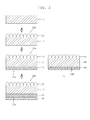
- FIG. 1 is a cross-sectional view showing a substrate for an organic light-emitting device (OLED) according to an embodiment of the present invention
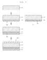
- FIG. 2 and FIG. 3 are process views sequentially showing a method of manufacturing a substrate for an OLED according to an embodiment of the present invention.
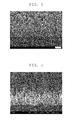
- FIG. 4 to FIG. 7 are scanning electron microscopy (SEM) pictures of the cross-section of a substrate for an OLED, in which the substrate is manufactured by the method of manufacturing a substrate for an OLED according to an embodiment of the present invention.
- a substrate 100 for an OLED is a substrate that is intended to improve the light extraction efficiency of the OLED.
- the substrate 100 is bonded to one surface of the OLED as one of a pair of substrates of the OLED which face each other.
- the substrate 100 serves as a passage through which light generated by the OLED is emitted to the outside while protecting the OLED from an external environment.
- the OLED has a multilayer structure that includes an anode, an organic light-emitting layer and a cathode which are disposed between the substrate 100 according to this embodiment of the present invention and an encapsulation substrate which opposes the substrate 100.
- the anode is formed as a part of the substrate 100 according to this embodiment of the present invention. This will be described in more detail later.
- the cathode is preferably implemented as a metal thin film of Al, Al:Li or Mg:Ag that has a low work function in order to facilitate injection of electrons, but not limited thereto.
- the cathode can have a multilayer structure that includes a semitransparent electrode of a metal thin film of Al, Al:Li or Mg:Ag and a transparent electrode of an oxide thin film of tin oxide (ITO) in order to facilitate transmission of light that is generated by the organic light-emitting layer.
- the organic light-emitting layer may include a hole injection layer, a hole carrier layer, a light-emitting layer, an electro carrier layer and an electron injection layer which are sequentially stacked on the anode.
- the substrate 100 for an OLED according to this embodiment of the present invention that is to be bonded to the OLED as described above includes a base substrate 110, a first metal oxide thin film 120, a second metal oxide thin film 130 and a third metal oxide thin film 140.
- the base substrate 110, the first metal oxide thin film 120, the second metal oxide thin film 130 and the third metal oxide thin film 140 are manufactured via in-line processing based on atmospheric pressure chemical vapor deposition (APCVD), thereby forming one package.
- APCVD atmospheric pressure chemical vapor deposition
- the base substrate 110 is a transparent substrate which can be made of any material without restrictions as long as it has superior light transmittance and excellent mechanical properties.
- the base substrate 110 can be made of a polymeric material such as a thermosetting or ultraviolet (UV)-curable organic film or a chemically tempered glass such as a soda-lime glass (SiO 2 -CaO-Na 2 O) or an aluminosilicate glass (SiO 2 -Al 2 O 3 -Na 2 O)
- soda-lime glass can be used when the OLED is used for illumination
- the aluminosilicate glass can be used when the OLED is used for a display.
- the base substrate 110 can be implemented as a thin glass having a thickness of 1.5 mm or less.
- the thin glass is made by a fusion process or a floating process.
- the first metal oxide thin film 120 is formed such that it coats one surface of the base substrate 110.
- the first metal oxide thin film 120 can coat the upper surface (with respect to the paper surface) of the base substrate 110.
- the (maximum) thickness of the (textured) first metal oxide thin film 120 that coats the upper surface of the base substrate 110 range from 0.2 to 5 ⁇ m.
- the first metal oxide thin film 120 can include a metal oxide, a solid solution of at least two metal oxides, or a multilayer structure of at least two metal oxides selected from the group consisting of ZnO, SnO 2 , SiO 2 , Al 2 O 3 and TiO 2 .
- a first texture 120a is formed on the surface of the first metal oxide thin film 120.
- the first texture 120a serves to scatter light in the visible light range, and can be patterned such that it has the shape of rods, half hexagons or hexagonal prisms or randomly-shaped features.
- the first texture 120a can be naturally formed when the first metal oxide thin film 120 is being deposited via APCVD. This will be described in more detail later in relation to a method of manufacturing a substrate for an OLED.
- the first metal oxide thin film 120 formed on the upper surface of the base substrate 110 is the outermost layer of the substrate 100 for an OLED, and serves as an outer light extraction layer of the OLED.
- the first metal oxide thin film 120 formed as the outer light extraction layer in this fashion has a haze value of 60% or more, a transmittance of 40% or more in the visible light range, and a refractive index ranging from 1.4 to 3.0.
- the second metal oxide thin film 130 is formed such that it coats the other surface of the base substrate 110, i.e. the undersurface (with respect to the paper surface) of the base substrate 110 that opposes the oxide thin film 120. It is preferred that the (maximum) thickness of the (textured) second metal oxide thin film 130 on the undersurface of the base substrate 110 range from 0.2 to 5 ⁇ m.
- the second metal oxide thin film 130 can be made of the same material as the first metal oxide thin film 120.
- the second metal oxide thin film 130 can include a metal oxide, a solid solution of at least two metal oxides, or a multilayer structure of at least two metal oxides selected from the group consisting of ZnO, SnO 2 , SiO 2 , Al 2 O 3 and TiO 2 .
- the second metal oxide thin film 130 has a second texture 130a on one surface thereof.
- the second texture 130a serves to scatter light, and can be patterned such that it has the shape of rods, rods having a half-hexagon at one side thereof or hexagonal prisms or randomly-shaped features.
- the surface of the second metal oxide thin film 130 on which the second texture 130a is formed adjoins the third metal oxide thin film 140.
- the second texture 130a can be naturally formed when the second metal oxide thin film 130 is being deposited via APCVD.
- one surface of the second metal oxide thin film 130 can form a flat surface.
- a planarization layer (not shown) can be formed on the surface of the second texture 130a, i.e. at the interface between the second metal oxide thin film 130 and the third metal oxide thin film 140.
- the planarization layer (not shown) is formed in the subsequent process, and is intended to guarantee the flatness of the third metal oxide thin film 140 which serves as the transparent electrode, or the anode, of the OLED.
- the second metal oxide thin film 130 can include a metal oxide, a solid solution of at least two metal oxides, or a multilayer structure of at least two metal oxides selected from the group consisting of ZnO, SnO 2 , SiO 2 , Al 2 O 3 and TiO 2 .
- the second metal oxide thin film 130 can include at least two metal oxides selected from the same group in which one metal oxide functions as a matrix and the other metal oxide is oversaturated, thereby precipitating as particles. In this case, the size of the particles range from 50 to 400 nm, and at least a minimum thickness that can contain the particles is required.
- the second metal oxide thin film 130 formed on the undersurface of the base substrate 110 serves as an inner light extraction layer of the OLED.
- the second metal oxide thin film 130 formed as the inner light extraction layer in this fashion has a haze value of 5% or more, a transmittance of 50% or more in the visible light range, and a refractive index ranging from 1.4 to 3.0.
- the third metal oxide thin film 140 is formed such that it coats the surface of the second metal oxide thin film 130. It is preferred that the thickness of the third metal oxide thin film 140 range from 50 to 2000 nm.
- the third metal oxide thin film 140 can include a metal oxide, a solid solution of at least two metal oxides, or a multilayer structure of at least two metal oxides selected from the group consisting of ZnO, SnO 2 , SiO 2 , Al 2 O 3 and TiO 2 .
- the third metal oxide thin film 140 must have electrical properties since it serves as a transparent electrode of the OLED.
- the metal oxides can include at least one of n-dopants including Ga, Al, F, Si and B and p-dopants including N. Accordingly, the third metal oxide thin film 140 has a sheet resistance of 15 ⁇ / ⁇ (15 Q).
- the third metal oxide thin film 140 forms a flat surface. Accordingly, the third metal oxide thin film 140, or the transparent electrode, has a haze value of 10% or less.
- the transparent electrode has a transmittance of 70% or more in the (preferably whole) visible light range and a refractive index ranging from 1.7 to 3.0 (for visible light).
- the method of manufacturing a substrate for an OLED according to this embodiment of the invention deposits at least one metal oxide thin film on each of one and the other surfaces of a base substrate via APCVD.
- APCVD atomic layer deposition
- a texture is naturally formed on the surface of the metal oxide thin film in the process in which the thin film is being deposited. That is, when the metal oxide thin film is formed via APCVD, it is possible to omit a process of forming the texture. This can consequently simplify the manufacturing process and improve productivity, thereby enabling mass production.
- the APCVD process is carried out under atmospheric pressure.
- This APCVD process includes loading the base substrate into a process chamber and then heating the base substrate to a predetermined temperature. Afterwards, a precursor gas and an oxidizer gas are blown into the process chamber in order to form the metal oxide thin film via APCVD. It is preferable to control the precursor gas and the oxidizer gas to be fed along different paths in order to prevent the gases from mixing before entering the process chamber.
- the precursor gas and the oxidizer gas can be preheated before being fed in order to promote a chemical reaction.
- the precursor gas can be fed on a carrier gas into the process chamber, the carrier gas being implemented as an inert gas such as nitrogen, helium or argon.
- the surface of the base substrate can be reformed via plasma treatment or chemical treatment before APCVD is started in order to control the shape of the texture that is formed on the surface of the metal oxide thin film.
- the method of manufacturing a substrate for an OLED using APCVD includes, first, the step of preparing the base substrate 110.
- the base substrate 110 can be made of a polymeric material such as a thermosetting or ultraviolet (UV)-curable organic film or a chemically tempered glass such as a soda-lime glass (SiO 2 -CaO-Na 2 O) or an aluminosilicate glass (SiO 2 -Al 2 O 3 -Na 2 O).
- the first metal oxide thin film 120 which is used as the outer light extraction layer of the OLED is formed on the upper surface of the base substrate 110 via deposition.
- at least one substance selected from the group of metal oxides consisting of ZnO, SnO 2 , SiO 2 , Al 2 O 3 and TiO 2 or a solid solution thereof can be used.
- the first texture 120a is naturally formed on the surface of the first metal oxide thin film 120.
- the second metal oxide thin film 130 which is used as the outer light extraction layer of the OLED is deposited on the undersurface of the base substrate 110.
- the second metal oxide thin film 130 at least one substance selected from the group of metal oxides consisting of ZnO, SnO 2 , SiO 2 , Al 2 O 3 and TiO 2 or a solid solution thereof can be used.
- the second texture 130a is naturally formed on the surface of the second metal oxide thin film 130.
- the planarization layer (not shown) be formed on the surface of the second texture 130a in order to guarantee the flatness of the third metal oxide thin film 140 which is to be formed in the subsequent process.
- the second metal oxide thin film 130 can include a metal oxide, a solid solution of at least two metal oxides, or a multilayer structure of at least two metal oxides selected from the group consisting of ZnO, SnO 2 , SiO 2 , Al 2 O 3 and TiO 2 .
- the second metal oxide thin film 130 can be formed such that one substance functions as a matrix and the other substance is oversaturated and precipitates as particles 130b.
- the size of the particles 130b ranges from 50 to 400 nm, and the matrix must have at least a minimum thickness such that the particles 130b can be formed therein.
- the third metal oxide thin film 140 which is used as the transparent electrode of the OLED is formed on the surface of the second metal oxide thin film 130 via deposition.
- at least one substance selected from the group of metal oxides consisting of ZnO, SnO 2 , SiO 2 , Al 2 O 3 and TiO 2 or a solid solution thereof can be used.
- the third metal oxide thin film 140 can be treated with at least one of n-dopants including Ga, Al, F, Si and B and p-dopants including N in order to make the third metal oxide thin film 140 be conductive.
- the manufacture of a substrate for an OLED according to this embodiment of the invention is completed.
- the above-described steps are carried out via in-line processing based on APCVD. It is therefore possible to simplify the thin film deposition processing which has been conducted by different processes in the related art, thereby decreasing a manufacturing cost and improving functional matchability.
- the first metal thin film 120 can be deposited after the second and third metal oxide thin films 130 and 140 are formed in advance.
Landscapes
- Physics & Mathematics (AREA)
- Optics & Photonics (AREA)
- Engineering & Computer Science (AREA)
- Manufacturing & Machinery (AREA)
- Electroluminescent Light Sources (AREA)
Applications Claiming Priority (1)
| Application Number | Priority Date | Filing Date | Title |
|---|---|---|---|
| KR1020120067315A KR101654360B1 (ko) | 2012-06-22 | 2012-06-22 | 유기 발광소자용 기판 및 그 제조방법 |
Publications (2)
| Publication Number | Publication Date |
|---|---|
| EP2704226A2 true EP2704226A2 (fr) | 2014-03-05 |
| EP2704226A3 EP2704226A3 (fr) | 2017-03-01 |
Family
ID=48651918
Family Applications (1)
| Application Number | Title | Priority Date | Filing Date |
|---|---|---|---|
| EP13173163.0A Withdrawn EP2704226A3 (fr) | 2012-06-22 | 2013-06-21 | Substrat pour OLED et son procédé de fabrication |
Country Status (4)
| Country | Link |
|---|---|
| US (1) | US20130341605A1 (fr) |
| EP (1) | EP2704226A3 (fr) |
| KR (1) | KR101654360B1 (fr) |
| CN (1) | CN103515541A (fr) |
Families Citing this family (10)
| Publication number | Priority date | Publication date | Assignee | Title |
|---|---|---|---|---|
| TWI495175B (zh) * | 2012-11-16 | 2015-08-01 | Au Optronics Corp | 有機電致發光元件 |
| KR101632614B1 (ko) * | 2014-12-24 | 2016-06-22 | 코닝정밀소재 주식회사 | 유기발광소자용 광추출 기판 제조방법, 유기발광소자용 광추출 기판 및 이를 포함하는 유기발광소자 |
| KR101762648B1 (ko) * | 2014-12-29 | 2017-07-31 | 코닝정밀소재 주식회사 | 유기발광소자용 광추출 기판 제조방법, 유기발광소자용 광추출 기판 및 이를 포함하는 유기발광소자 |
| CN105280838B (zh) * | 2015-09-22 | 2017-08-25 | 深圳市华星光电技术有限公司 | 一种oled发光器件及显示装置 |
| CN105244453B (zh) * | 2015-09-22 | 2017-08-25 | 深圳市华星光电技术有限公司 | 一种有机发光器件 |
| JP6871705B2 (ja) * | 2016-09-29 | 2021-05-12 | デクセリアルズ株式会社 | 光学体、光学体の製造方法、および発光装置 |
| TWI605288B (zh) | 2017-01-16 | 2017-11-11 | 友達光電股份有限公司 | 畫素結構與具有此畫素結構的顯示面板 |
| CN106981581A (zh) * | 2017-02-08 | 2017-07-25 | 广东工业大学 | 一种提高光取出率的有机电致发光器件 |
| KR102831416B1 (ko) * | 2023-03-10 | 2025-07-08 | 고려대학교 산학협력단 | 금속산화물 투명기판 및 그 제조방법 |
| WO2024191121A1 (fr) * | 2023-03-10 | 2024-09-19 | 고려대학교 산학협력단 | Substrat d'oxyde métallique transparent et son procédé de fabrication |
Family Cites Families (18)
| Publication number | Priority date | Publication date | Assignee | Title |
|---|---|---|---|---|
| CN1633826A (zh) * | 2001-09-12 | 2005-06-29 | 日产化学工业株式会社 | 有机电致发光元件用透明基板及元件 |
| JP4389585B2 (ja) * | 2001-10-19 | 2009-12-24 | 旭硝子株式会社 | 透明導電性酸化物膜付き基体および光電変換素子 |
| US7151532B2 (en) * | 2002-08-09 | 2006-12-19 | 3M Innovative Properties Company | Multifunctional multilayer optical film |
| JP2005038681A (ja) * | 2003-07-18 | 2005-02-10 | Toyota Industries Corp | ボトムエミッション型発光素子形成用の透明基板及び当該透明基板を用いた発光デバイス |
| US20060040067A1 (en) * | 2004-08-23 | 2006-02-23 | Thomas Culp | Discharge-enhanced atmospheric pressure chemical vapor deposition |
| JP2006066264A (ja) * | 2004-08-27 | 2006-03-09 | Fuji Photo Film Co Ltd | 有機電界発光素子、プリズム構造体付き基板の作成方法、及びプリズム構造体付き基板を用いた有機電界発光素子の製造方法 |
| JP5261397B2 (ja) * | 2006-11-17 | 2013-08-14 | サン−ゴバン グラス フランス | 有機発光素子用の電極、その酸エッチング、及び、それを組み込んだ有機発光素子 |
| US7911133B2 (en) * | 2007-05-10 | 2011-03-22 | Global Oled Technology Llc | Electroluminescent device having improved light output |
| KR101548025B1 (ko) * | 2007-07-27 | 2015-08-27 | 아사히 가라스 가부시키가이샤 | 투광성 기판, 그의 제조 방법, 유기 led 소자 및 그의 제조 방법 |
| EP2203030A4 (fr) * | 2007-08-27 | 2010-09-29 | Panasonic Elec Works Co Ltd | Élément électroluminescent organique |
| KR20100043517A (ko) * | 2008-10-20 | 2010-04-29 | 엘지디스플레이 주식회사 | 금속산화물전극의 제조방법과 이를 이용한 유기전계발광표시장치 |
| KR20120003859A (ko) * | 2009-03-17 | 2012-01-11 | 아이엠이씨 | 플라즈마 텍스처링 방법 |
| KR20100130019A (ko) * | 2009-06-02 | 2010-12-10 | 삼성전자주식회사 | 금속 산화물층의 제조 방법, 상기 방법을 이용하여 제조한 박막 트랜지스터 기판 및 그 제조 방법 |
| US10581020B2 (en) * | 2011-02-08 | 2020-03-03 | Vitro Flat Glass Llc | Light extracting substrate for organic light emitting diode |
| KR101163647B1 (ko) * | 2010-05-27 | 2012-07-09 | 순천대학교 산학협력단 | 투명전도막 및 그 제조방법 |
| US20140042422A1 (en) * | 2011-04-12 | 2014-02-13 | Battelle Memorial Institute | Internal optical extraction layer for oled devices |
| EP2518789B1 (fr) * | 2011-04-18 | 2016-04-13 | Corning Precision Materials Co., Ltd. | Procédé de fabrication d'un substrat d'extraction de lumière pour un dispositif électroluminescent |
| CN102299266A (zh) * | 2011-09-15 | 2011-12-28 | 四川虹视显示技术有限公司 | 有机电致发光器件的基板及制造方法 |
-
2012
- 2012-06-22 KR KR1020120067315A patent/KR101654360B1/ko active Active
-
2013
- 2013-06-19 US US13/921,294 patent/US20130341605A1/en not_active Abandoned
- 2013-06-21 EP EP13173163.0A patent/EP2704226A3/fr not_active Withdrawn
- 2013-06-24 CN CN201310252902.XA patent/CN103515541A/zh active Pending
Non-Patent Citations (1)
| Title |
|---|
| None |
Also Published As
| Publication number | Publication date |
|---|---|
| EP2704226A3 (fr) | 2017-03-01 |
| US20130341605A1 (en) | 2013-12-26 |
| CN103515541A (zh) | 2014-01-15 |
| KR101654360B1 (ko) | 2016-09-05 |
| KR20140000426A (ko) | 2014-01-03 |
Similar Documents
| Publication | Publication Date | Title |
|---|---|---|
| EP2704226A2 (fr) | Substrat pour OLED et son procédé de fabrication | |
| KR102894711B1 (ko) | 광 투과 영역을 포함하는 광전자 디바이스 | |
| CN106654046A (zh) | Oled显示面板及其制作方法 | |
| EP3185249B1 (fr) | Électrode transparente, procédé de production d'électrode transparente et dispositif électronique | |
| US20140349070A1 (en) | Reflective anode electrode for use in an organic electroluminescent display and method for making the same | |
| CN106538060A (zh) | 有机电场发光元件 | |
| US9464351B2 (en) | Method of fabricating light-scattering substrate | |
| CN105518896B (zh) | 用于制造超薄有机发光装置的方法 | |
| EP3200195A1 (fr) | Substrat flexible et son procédé de fabrication | |
| KR101765183B1 (ko) | 발광장치용 광추출층 및 그 형성방법 | |
| US9711762B2 (en) | Substrate for organic light-emitting diode, method for manufacturing same, and organic light-emitting diode comprising same | |
| CN112259693A (zh) | 显示面板及其制作方法 | |
| US9825257B2 (en) | Light extraction substrate for OLED and method of fabricating the same | |
| JP6340674B2 (ja) | 有機発光素子用の光取出し基板、その製造方法、及びこれを含む有機発光素子 | |
| US20170358763A1 (en) | Flexible substrate and method of manufacturing same | |
| KR101604495B1 (ko) | 유기발광다이오드 표시장치 및 이를 제조하는 방법 | |
| KR101699275B1 (ko) | 유기발광소자용 광추출 기판, 그 제조방법 및 이를 포함하는 유기발광소자 | |
| JP2002352962A (ja) | 有機発光素子およびその製造方法、有機発光表示装置および照明装置 | |
| JP6330543B2 (ja) | 透明電極、及び、電子デバイス | |
| EP2725634B1 (fr) | Procédé de fabrication de substrat d'extraction de lumière à diode électroluminescente organique | |
| CN203746913U (zh) | 有机发光二极管结构 |
Legal Events
| Date | Code | Title | Description |
|---|---|---|---|
| AK | Designated contracting states |
Kind code of ref document: A2 Designated state(s): AL AT BE BG CH CY CZ DE DK EE ES FI FR GB GR HR HU IE IS IT LI LT LU LV MC MK MT NL NO PL PT RO RS SE SI SK SM TR |
|
| AX | Request for extension of the european patent |
Extension state: BA ME |
|
| PUAI | Public reference made under article 153(3) epc to a published international application that has entered the european phase |
Free format text: ORIGINAL CODE: 0009012 |
|
| RAP1 | Party data changed (applicant data changed or rights of an application transferred) |
Owner name: CORNING PRECISION MATERIALS CO., LTD. |
|
| PUAL | Search report despatched |
Free format text: ORIGINAL CODE: 0009013 |
|
| AK | Designated contracting states |
Kind code of ref document: A3 Designated state(s): AL AT BE BG CH CY CZ DE DK EE ES FI FR GB GR HR HU IE IS IT LI LT LU LV MC MK MT NL NO PL PT RO RS SE SI SK SM TR |
|
| AX | Request for extension of the european patent |
Extension state: BA ME |
|
| RIC1 | Information provided on ipc code assigned before grant |
Ipc: H01L 51/52 20060101AFI20170126BHEP |
|
| STAA | Information on the status of an ep patent application or granted ep patent |
Free format text: STATUS: THE APPLICATION HAS BEEN PUBLISHED |
|
| STAA | Information on the status of an ep patent application or granted ep patent |
Free format text: STATUS: THE APPLICATION IS DEEMED TO BE WITHDRAWN |
|
| 18D | Application deemed to be withdrawn |
Effective date: 20170902 |