EP2704257A1 - Antenne mit drei Frequenzbändern und entsprechendes Verfahren - Google Patents
Antenne mit drei Frequenzbändern und entsprechendes Verfahren Download PDFInfo
- Publication number
- EP2704257A1 EP2704257A1 EP13182971.5A EP13182971A EP2704257A1 EP 2704257 A1 EP2704257 A1 EP 2704257A1 EP 13182971 A EP13182971 A EP 13182971A EP 2704257 A1 EP2704257 A1 EP 2704257A1
- Authority
- EP
- European Patent Office
- Prior art keywords
- edge
- sub
- path
- conductor branch
- terminal
- Prior art date
- Legal status (The legal status is an assumption and is not a legal conclusion. Google has not performed a legal analysis and makes no representation as to the accuracy of the status listed.)
- Withdrawn
Links
Images



Classifications
-
- H—ELECTRICITY
- H01—ELECTRIC ELEMENTS
- H01Q—ANTENNAS, i.e. RADIO AERIALS
- H01Q9/00—Electrically-short antennas having dimensions not more than twice the operating wavelength and consisting of conductive active radiating elements
- H01Q9/04—Resonant antennas
-
- H—ELECTRICITY
- H01—ELECTRIC ELEMENTS
- H01Q—ANTENNAS, i.e. RADIO AERIALS
- H01Q1/00—Details of, or arrangements associated with, antennas
- H01Q1/12—Supports; Mounting means
- H01Q1/22—Supports; Mounting means by structural association with other equipment or articles
- H01Q1/24—Supports; Mounting means by structural association with other equipment or articles with receiving set
- H01Q1/241—Supports; Mounting means by structural association with other equipment or articles with receiving set used in mobile communications, e.g. GSM
- H01Q1/242—Supports; Mounting means by structural association with other equipment or articles with receiving set used in mobile communications, e.g. GSM specially adapted for hand-held use
- H01Q1/243—Supports; Mounting means by structural association with other equipment or articles with receiving set used in mobile communications, e.g. GSM specially adapted for hand-held use with built-in antennas
-
- H—ELECTRICITY
- H01—ELECTRIC ELEMENTS
- H01Q—ANTENNAS, i.e. RADIO AERIALS
- H01Q5/00—Arrangements for simultaneous operation of antennas on two or more different wavebands, e.g. dual-band or multi-band arrangements
- H01Q5/30—Arrangements for providing operation on different wavebands
- H01Q5/307—Individual or coupled radiating elements, each element being fed in an unspecified way
- H01Q5/342—Individual or coupled radiating elements, each element being fed in an unspecified way for different propagation modes
- H01Q5/357—Individual or coupled radiating elements, each element being fed in an unspecified way for different propagation modes using a single feed point
- H01Q5/364—Creating multiple current paths
- H01Q5/371—Branching current paths
-
- H—ELECTRICITY
- H01—ELECTRIC ELEMENTS
- H01Q—ANTENNAS, i.e. RADIO AERIALS
- H01Q9/00—Electrically-short antennas having dimensions not more than twice the operating wavelength and consisting of conductive active radiating elements
- H01Q9/04—Resonant antennas
- H01Q9/0407—Substantially flat resonant element parallel to ground plane, e.g. patch antenna
- H01Q9/0421—Substantially flat resonant element parallel to ground plane, e.g. patch antenna with a shorting wall or a shorting pin at one end of the element
-
- H—ELECTRICITY
- H01—ELECTRIC ELEMENTS
- H01Q—ANTENNAS, i.e. RADIO AERIALS
- H01Q9/00—Electrically-short antennas having dimensions not more than twice the operating wavelength and consisting of conductive active radiating elements
- H01Q9/04—Resonant antennas
- H01Q9/30—Resonant antennas with feed to end of elongated active element, e.g. unipole
- H01Q9/40—Element having extended radiating surface
-
- H—ELECTRICITY
- H01—ELECTRIC ELEMENTS
- H01Q—ANTENNAS, i.e. RADIO AERIALS
- H01Q9/00—Electrically-short antennas having dimensions not more than twice the operating wavelength and consisting of conductive active radiating elements
- H01Q9/04—Resonant antennas
- H01Q9/30—Resonant antennas with feed to end of elongated active element, e.g. unipole
- H01Q9/42—Resonant antennas with feed to end of elongated active element, e.g. unipole with folded element, the folded parts being spaced apart a small fraction of the operating wavelength
-
- Y—GENERAL TAGGING OF NEW TECHNOLOGICAL DEVELOPMENTS; GENERAL TAGGING OF CROSS-SECTIONAL TECHNOLOGIES SPANNING OVER SEVERAL SECTIONS OF THE IPC; TECHNICAL SUBJECTS COVERED BY FORMER USPC CROSS-REFERENCE ART COLLECTIONS [XRACs] AND DIGESTS
- Y10—TECHNICAL SUBJECTS COVERED BY FORMER USPC
- Y10T—TECHNICAL SUBJECTS COVERED BY FORMER US CLASSIFICATION
- Y10T29/00—Metal working
- Y10T29/49—Method of mechanical manufacture
- Y10T29/49002—Electrical device making
- Y10T29/49016—Antenna or wave energy "plumbing" making
Definitions
- the present disclosure relates to an antenna structure and, more particularly, relates to an antenna structure having plural operating frequency bands.
- the handheld electronic device is a mobile phone or a notebook computer
- the wireless transmission device is an access point, a wireless network card or a wireless card bus.
- the existing planar inverted F antenna (PIFA) or the existing monopole antenna has a handy-sized structure and a satisfactory transmission performance, can be easily disposed on the inner wall of the handheld electronic device, and is widely applied in wireless transmission devices of handheld electronic devices, notebook computers or wireless communication devices.
- a PIFA capable to be applied to a multi-frequency system has properties including a complex structure and uneasy adjustments to the respective frequency bands.
- the issued TW patent with No. I351,787 discloses a triple band antenna in the prior art.
- the issued TW patent with No. I333,715 discloses a miniaturized triple-band diamond coplanar waveguide antenna in the prior art.
- the issued US patent with No. 7,256,743 B2 discloses an internal multi-band antenna in the prior art.
- the issued US patent with No. 7,242,352 B2 discloses a multi-band or wide-band antenna in the prior art.
- the antenna structure includes a radiation portion.
- the radiation portion includes a first conductor branch path, a second conductor branch path and a third conductor branch path.
- the second conductor branch path is electrically connected to the first conductor branch path.
- the third conductor branch path includes a first extension portion extending from the second conductor branch path.
- One of the second and the third conductor branch paths is a longest one of the first, the second and the third conductor branch paths.
- the longest path includes a shared area covering more than one-third of an area of the longest path.
- the second branch path overlaps the third conductor branch path in the shared area.
- a substrate is provided.
- a ground portion and a radiation portion having three conductor branch paths are formed on the substrate, wherein one of the three conductor branch paths includes a specific portion having an extension direction.
- a short-circuit conductor portion is disposed between the ground portion and the radiation portion, wherein the short-circuit conductor portion includes a body having a longitudinal axis, and an extension portion extending from the body in a first inclination direction, and the first inclination direction and the extension direction are located on different sides relative to the longitudinal axis.
- a relationship between the longitudinal axis and at least one of the first inclination direction and the extension direction is determined so as to cause the antenna to have a predetermined impedance match.
- the antenna includes a radiation portion.
- the radiation portion includes a feed terminal and three conductor branch paths directly extending from the feed terminal.
- the three conductor branch paths are located on the same side of the feed terminal, and each has an initial direction, and any two of the three initial directions have an acute angle therebetween.
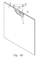
- Fig. 1A , Fig. 1B and Fig. 1C are schematic diagrams respectively showing a front view, an equal-angle projection view and a detail front view of an antenna structure according to some embodiments of the present disclosure
- Fig. 1D is a representation of Fig. 1C without reference numerals.
- Fig. 2 is a test result graph showing a voltage standing wave ratio (VSWR) of the antenna structure in Figs. 1A , 1B and 1C .
- VSWR voltage standing wave ratio
- Fig. 1A , Fig. 1B and Fig. 1C are schematic diagrams respectively showing a front view, an equal-angle projection view and a detail front view of an antenna structure 20 according to some embodiments of the present disclosure.
- Fig. 1D is a representation of Fig. 1C without reference numerals.
- the antenna structure (or an antenna) 20 includes a radiation portion 30.
- the radiation portion 30 includes a feed terminal 35 and three conductor branch paths 31, 32 and 33 directly extending from the feed terminal 35.
- the three conductor branch paths 31, 32 and 33 are located on the same side of the feed terminal 35, and each has an initial direction, and any two of the three initial directions 31D, 32D and 33D have an acute angle DR1 therebetween.
- the antenna structure 20 has three operating frequency bands FB1, FB2 and FB3; the three conductor branch paths 31, 32 and 33 respectively have three initial directions 31D, 32D and 33D; and the included angle DR1 between any two of the three initial directions 31D, 32D and 33D is less than 90°.
- the acute angle DR1 has an angle value being in a range between 0° and 90°.
- the acute angle DR1 has an angle value being in one of the following ranges: between 0° and 80°, or between 0° and 70°, or between 0° and 55°, or between 0° and 60°, or in particular between 0° and 65°.
- the conductor branch path 31 directly extending from the feed terminal 35 to a terminal position TP1, and has a length LT1, an extension direction 31A from the feed terminal 35 to the terminal position TP1, an edge EA1 and edge EA2 opposite to the edge EA1.
- the conductor branch path 32 is electrically connected to the conductor branch path 31, and includes a length LT2.
- the conductor branch path 33 has a length LT3.
- One of the conductor branch paths 32 and 33 is a longest path (such as the conductor branch path 33) of the conductor branch paths 31, 32 and 33.
- the longest path (such as the conductor branch path 33) includes a shared area QC1 covering more than one-third of an area of the longest path.
- the conductor branch paths 32 and 33 share the shared area QC1; that is, the conductor branch path 32 overlaps the conductor branch path 33 in the shared area QC1.
- a shared conductor branch path 34 includes a part of the conductor branch path 32 and a part of the conductor branch path 33, occupies the shared area QC1, and has a length LT4.
- the length LT4 is greater than one-third of the length LT3.
- the shared area QC1 covers more than half of the longest path; and the extension direction 31A is close to or aligned with the initial direction 31D.
- the length LT4 is greater than half of the length LT3.
- the conductor branch path 32 and the conductor branch path 33 share the shared conductor branch path 34.
- the part of the conductor branch path 32 and the part of the conductor branch path 33 overlap to form the shared conductor branch path 34.
- the shared conductor branch path 34 directly extends from the feed terminal 35 to a node ND1, and further has an initial extension portion 341, a corner position CP1, an extension direction 34A from the feed terminal 35 to the corner position CP1, a sub-path 342 between the initial extension portion 341 and the corner position CP1, and a sub-path 343 between the corner position CP1 and the node ND1.
- the initial extension portion 341 includes a side 3411 relative to the feed terminal 35 and a side 3412 opposite to the side 3411, wherein the side 3411 is coupled to the conductor branch path 31, and the side 3412 includes a short-circuiting terminal SC1.
- the extension direction 34A is close to or aligned with each of the initial directions 32D and 33D.
- the sub-path 342 includes an edge EB1 and an edge EB2 opposite to the edge EB1.
- the sub-path 343 includes an edge EC1 and an edge EC2 opposite to the edge EC1.
- the extension directions 31A and 34A includes an acute angle therebetween; and the shared area QC1 extends from the short-circuiting terminal SC1, the feed terminal 35 and the conductor branch path 31.
- the initial direction 32D is aligned with the initial direction 33D; and the initial directions 31D and 32D have a specific included angle therebetween having an angle value being in a range between 30° and 90°.
- the specific included angle has an angle value being in one of the following ranges: between 45° and 75°, or between 50° and 70°, or in particular between 55° and 65°.
- the conductor branch path 32 includes the shared conductor branch path 34 and an extension portion 321 extending from the node ND1 to a terminal position TP2.
- the extension portion 321 includes a corner position CP2, and a sub-path 3211 between the corner position CP2 and the terminal position TP2.
- the sub-path 3211 includes an edge ED1 and an edge ED2 opposite to the edge ED1.
- the extension portion 321 forms an included angle, close to or being a right angle, at the corner position CP2 by making a turn.
- the conductor branch path 33 includes the shared conductor branch path 34 and an extension portion 331 extending from the node ND1 to a terminal position TP3.
- the extension portion 331 includes a corner position CP3, and a sub-path 3311 between the corner position CP3 and the terminal position TP3.
- the sub-path 3311 includes an edge EE1 and an edge EE2 opposite to the edge EE1.
- the extension portion 331 forms an included angle, close to or being a right angle, at the corner position CP3 by making a turn.
- the antenna structure 20 further includes a substrate 21, a ground portion 22, a short-circuit conductor portion 23, a gap structure 24, a gap structure 25 and a feed connection portion 26.
- the substrate 21 includes a surface 211, wherein the surface 211 includes an edge EF1, a side portion 2111 adjacent to the edge EF1, and a body portion 2112 partially surrounding the side portion 2111, and the radiation portion 30 is disposed on the side portion 2111.
- the substrate 21 is a dielectric substrate.
- the feed connection portion 26 is electrically connected between the feed terminal 35 and a module terminal (not shown), and has a specific impedance.
- the module terminal is an antenna port, and the specific impedance is equal to 50 ⁇ or 75 ⁇ .
- the feed connection portion 26 is a cable.
- the ground portion 22 is disposed on the body portion 2112, and includes a corner position CP4 adjacent to the edge EF1 of the substrate 21, a corner position CP5 adjacent to the edge EF1 of the substrate 21, a short-circuiting terminal SC2 at a distance DT11 from the corner position CP4, an edge EG1 partially surrounding the radiation portion 30 and located between the corner position CP4 and the short-circuiting terminal SC2, and an edge EG2 partially surrounding the radiation portion 30 and located between the corner position CP5 and the short-circuiting terminal SC2, wherein the corner position CP4 is opposite to the corner position CP4 in respect to the radiation portion 30.
- the short-circuit conductor portion 23 extends from the short-circuiting terminal SC2 to the short-circuiting terminal SC1, and includes a corner position CP6, a body 231 between the short-circuiting terminal SC2 and the corner position CP6, an extension portion 232 between the corner position CP6 and the short-circuiting terminal SC1, and an extension direction 23A from the corner position CP6 to the short-circuiting terminal SC1.
- the body 231 of the short-circuit conductor portion 23 includes an edge EH1, an edge EH2 opposite to the edge EH1, and a longitudinal axis AX1 with a longitudinal axis direction AX1A, wherein the longitudinal axis AX1 passes through the short-circuiting terminal SC2.
- the extension portion 232 includes an edge EK1, an edge EK2 opposite to the edge EK1.
- the extension direction 23A is an inclination direction 23B; the short-circuit conductor portion 23 forms an obtuse angle at the corner position CP6 by making a turn;
- the longitudinal axis AX1 is parallel or nearly parallel to the edge EA2; and the longitudinal axis AX1 is perpendicular or nearly perpendicular to the edge EB2.
- the longitudinal axis AX1 is parallel or nearly parallel to the edge EC1; and the edges EB1 and EC1 have an obtuse angle therebetween.
- the gap structure 24 is disposed among the edge EG1 of the ground portion 22, the short-circuit conductor portion 23 and the shared conductor branch path 34.
- the gap structure 25 is disposed among the short-circuit conductor portion 23, the radiation portion 30 and the edge EG2 of the ground portion 22.
- the gap structures 24 and 25 are interconnected.
- the gap structure 24 is disposed among the edge EG1 of the ground portion 22, the short-circuit conductor portion 23 and the sub-path 342.
- the radiation portion 30, the ground portion 22 and the short-circuit conductor portion 23 is coplanar.
- the edge EG2 of the ground portion 22 includes a sub-edge EG21 having a bottom height, a sub-edge EG22 having a middle height, a sub-edge EG23 between the corner position CP5 and the sub-edge EG21, a sub-edge EG24 between the sub-edge EG21 and the sub-edge EG22, and a sub-edge EG25 between the short-circuiting terminal SC2 and the sub-edge EG22.
- a distance between the sub-edge EG21 and the edge EF1 is longer than a distance between the sub-edge EG22 and the edge EF1.
- the gap structure 25 includes four gaps 251, 252, 253 and 254.
- the gap 251 is disposed among the short-circuit conductor portion 23, the conductor branch path 31, the sub-edge EG21, the sub-edge EG24, the sub-edge EG22 and the sub-edge EG25.
- the gap 252 is disposed between the conductor branch paths 31 and 32.
- the gap 253 is disposed between the sub-path 3311 and the sub-edge EG23.
- the gap 254 is disposed between the extension portion 331 and the sub-edge EG21.
- the edge EH1 of the body 231 and the edge EF1 of the substrate 21 have a distance DT12 therebetween.
- the edge EH2 of the body 231 and the sub-edge EG22 have a distance DT13 therebetween.
- the feed terminal 35 and the sub-edge EG24 have a distance DT14 therebetween.
- the edge EA2 of the conductor branch path 31 and the sub-edge EG21 have a distance DT15 therebetween.
- the terminal position TP1 and the edge EE1 of the sub-path 3311 have a distance DT16 therebetween.
- the edge EA1 of the conductor branch path 31 and the edge ED2 of the sub-path 3211 have a distance DT17 therebetween.
- the edge ED1 of the sub-path 3211 and the edge EC2 of the sub-path 343 have a distance DT18 therebetween.
- the terminal position TP2 and the edge EB2 of the sub-path 342 have a distance DT19 therebetween.
- the edge EE2 of the sub-path 3311 and the sub-edge EG23 have a distance DT20 therebetween.
- the terminal position TP3 and the edge EA2 of the conductor branch path 31 have a distance DT21 therebetween.
- the feed terminal 35 and the longitudinal axis AX1 have a distance DT22 therebetween.
- the distances DT12, DT13, DT14, DT15, DT16, DT17, DT18, DT19, DT20, DT21 and DT22 are eleven perpendicular distances.
- the longitudinal axis direction AX1A and the extension direction 34A have an included angle AG1 therebetween.
- the longitudinal axis direction AX1A and the extension direction 23A have an included angle AG2 therebetween.
- the included angles AG1 and AG2 are two acute angles, respectively.
- a ratio of the included angle AG1 to the included angle AG2 has a value being in a range between 1.0 and 3.0; and especially, the ratio has a value being in one of the following ranges: between 1.5 and 2.5, or in particular between 1.8 and 2.2.
- the included angle AG2 has an angle value being in a range between 5° and 61°.
- the included angle AG2 has an angle value being in one of the following ranges: between 15° and 51°, or between 24° and 42°, or between 28° and 39°, or in particular between 30° and 36°.
- the antenna structure 20 uses the conductor branch paths 31, 32 and 33 to respectively form operating frequency bands FB1, FB2 and FB3.
- the distance DT16 is changeable to cause the operating frequency band FB1 to be movable.
- the distance DT19 is changeable to cause the operating frequency band FB2 to be movable.
- the distance DT21 is changeable to cause the operating frequency band FB3 to be movable. For instance, the distance DT21 is changed to cause the operating frequency band FB3 to move from a first specific frequency band to a second specific frequency band.
- the distance DT19 is changed to cause the operating frequency band FB2 to move from a third specific frequency band to a fourth specific frequency band.
- the distance DT16 is changed to cause the operating frequency band FB1 to move from a fifth specific frequency band to a sixth specific frequency band.
- the operating frequency bands FB1, FB2 and FB3 are determined by the conductor branch paths 31, 32 and 33 respectively.
- the operating frequency band FB1 changes with the distance DT16.
- the operating frequency band FB2 changes with the distance DT19.
- the operating frequency band FB3 changes with the distance DT21.
- the antenna structure 20 makes a predetermined impedance match in response to a change of one being selected from a group consisting of the distances DT12, DT13, DT14, DT15, DT17, DT18, DT20 and DT22, the included angles AG1 and AG2 and a combination thereof.
- the antenna structure 20 includes a wire structure 28, which includes the radiation portion 30 and the short-circuit conductor portion 23. At least one selected from a group consisting of the distances DT12, DT13, DT14, DT15, DT17, DT18, DT20 and DT22, and the included angles AG1 and AG2 is changeable to cause the antenna structure 20 to have a predetermined impedance match.
- the wire structure 28 has an impedance R1; and at least one selected from a group consisting of the distances DT12, DT13, DT14, DT15, DT17, DT18, DT20 and DT22, and the included angles AG1 and AG2 is changeable to change the impedance R1, thereby causing the antenna structure 20 to have the predetermined impedance match.
- the predetermined impedance match is associated with the impedance R1 and the feed connection portion 26.
- the longitudinal axis direction AX1A and the edge EB1 have an included angle AG3 (denoted through a translation) therebetween; the longitudinal axis direction AX1A and the edge EK1 have an included angle AG4 (denoted through a translation) therebetween; and the longitudinal axis direction AX1A and the edge EK2 have an included angle AG5 therebetween.
- At least one selected from a group consisting of the distances DT12, DT13, DT14, DT15, DT17, DT18, DT20 and DT22, and the included angles AG1, AG2, AG3, AG4 and AG5 is changeable to cause the antenna structure 20 to have a predetermined impedance match.
- the antenna structure 20 makes a predetermined impedance match in response to a change of one being selected from a group consisting of the distances DT12, DT13, DT14, DT15, DT17, DT18, DT20 and DT22, the included angles AG1, AG2, AG3, AG4 and AG5 and a combination thereof.
- an antenna structure 20 having three operating frequency bands FB1, FB2 and FB3 includes a radiation portion 30, which includes conductor branch paths 31, 32 and 33.
- the conductor branch path 32 is electrically connected to the conductor branch path 31; and the conductor branch path 33 includes an extension portion 331 extending from the conductor branch path 32.
- One of the conductor branch paths 32 and 33 is a longest one (such as the conductor branch path 33) of the conductor branch paths 31, 32 and 33.
- the longest path (such as the conductor branch path 33) includes a shared area QC1 covering more than one-third of an area of the longest path; and the conductor branch path 32 overlaps the conductor branch path 33 in the shared area QC1.
- a method for manufacturing an antenna structure (or an antenna) 20 having three operating frequency bands FB1, FB2 and FB3 includes the following steps.
- a substrate 21 is provided.
- a ground portion 22 and a radiation portion 30 having three conductor branch paths 31, 32 and 33 are formed on the substrate 21, wherein one of the three conductor branch paths 31, 32 and 33 includes a specific portion (including the initial extension portion 341 and the sub-path 342, for example) having an extension direction 34A.
- a short-circuit conductor portion 23 is disposed between the ground portion 22 and the radiation portion 30, wherein the short-circuit conductor portion 23 includes a body 231 having a longitudinal axis AX1, and an extension portion 232 extending from the body 231 in an inclination direction 23B, and the inclination direction 23B and the extension direction 34A are located on different sides relative to the longitudinal axis AX1.
- a relationship between the longitudinal axis AX1 and at least one of the inclination direction 23B and the extension direction 34A is determined so as to cause the antenna structure 20 to have a predetermined impedance match.
- the radiation portion 30 further has a feed terminal 35 and a centroid HC1.
- the conductor branch path 31 directly extends from the feed terminal 35 to a terminal position TP1, and includes an outer edge (such as the edge EA2) relative to the centroid HC1.
- a shared conductor branch path 34 includes a part of the conductor branch path 32 and a part of the conductor branch path 33, directly extends from the feed terminal 35 to a node ND1, and includes an initial extension portion 341, a corner position CP1 and a sub-path 342 between the initial extension portion 341 and the corner position CP1.
- the sub-path 342 includes a first inner edge (such as the edge EB2) relative to the centroid HC1.
- the conductor branch path 32 includes the shared conductor branch path 34 and an extension portion 321 extending from the node ND1 to a terminal position TP2, wherein the extension portion 321 includes a corner position CP2.
- the conductor branch path 33 includes the shared conductor branch path 34 and an extension portion 331 extending from the node ND1 to a terminal position TP3.
- the part of the conductor branch path 32 and the part of the conductor branch path 33 overlap to form the shared conductor branch path 34.
- the extension portion 331 includes a corner position CP3 and a sub-path 3311 between the corner position CP3 and the terminal position TP3, wherein the sub-path 3311 includes a second inner edge (such as the edge EE1) relative to the centroid HC1.
- the terminal position TP1 and the second inner edge (such as the edge EE1) have a first perpendicular distance (such as the distance DT16) therebetween.
- the terminal position TP2 and the first inner edge (such as the edge EB2) have a second perpendicular distance (such as the distance DT19) therebetween.
- the terminal position TP3 and the outer edge (such as the edge EA2) have a third perpendicular distance (such as the distance DT21) therebetween.
- the method for manufacturing the antenna structure 20 further includes the following steps.
- the conductor branch paths 31, 32 and 33 are used to respectively form the operating frequency bands FB1, FB2 and FB3.
- the first operating frequency band FB1 is obtained by adjusting the first perpendicular distance (such as the distance DT16).
- the second operating frequency band FB2 is obtained by adjusting the second perpendicular distance (such as the distance DT19).
- the third operating frequency band FB3 is obtained by adjusting the third perpendicular distance (such as the distance DT21).
- the antenna structure 20 is a printed antenna structure, and is used in a wireless transmission device (not shown).
- the antenna structure 20 is used on a printed circuit board, has a geometrical structure to be adjusted easily, and can be applied to a specific device (such as a wireless communication device), which has a system frequency band demand for the operating frequency bands LTE-Band 20 (790 ⁇ 870MHz), LTE-Band 3 (1770 ⁇ 1880MHz) and LTE-Band 7 (2500 ⁇ 2700MHz).
- the wireless communication device is a notebook computer, a mobile phone, an access point, or a device of a television or a digital video disk, which includes the Wi-Fi technique.
- the antenna structure 20 may be applied to the LTE (Long Term Evolution) system employing Band 20, Band 3 and Band 7.
- the bands of the antenna structure 20 may be slightly adjusted to cause the antenna structure 20 to be applied to another wireless communication system employing three operating frequency bands.
- the antenna structure 20 includes a conductive structure (including the radiation portion 30, the ground portion 22 and the short-circuit conductor portion 23), which is directly printed on a substrate 21 (such as a circuit board), thereby being able to reduce the mold cost and the production assembly cost relative to the three-dimensional antenna and being applied to wireless network devices in various environments.
- a conductive structure including the radiation portion 30, the ground portion 22 and the short-circuit conductor portion 23
- a substrate 21 such as a circuit board
- the antenna structure 20 is a PITA antenna structure, and includes the substrate 21, the ground portion 22 and a wire structure 28.
- the wire structure 28 is a microstrip line, is printed on the side portion 2111, and includes the feed terminal 35 and the short-circuiting terminal SC2.
- the feed terminal 35 serves as a signal feed-in terminal
- the short-circuiting terminal SC2 serves as a signal grounding terminal.
- the substrate 21 further includes a reverse side opposite to the surface 211.
- the reverse side has a first surface portion and a second surface portion.
- the first surface portion corresponds to the side portion 2111, and is not printed with a ground metal surface.
- the second surface portion corresponds to the wire structure 28, and may be printed with a ground metal surface (under a three-laminate board condition) or may be completely no metal (under a two-laminate board condition).
- the antenna structure 20 is built in a wireless transmission device.
- the radiation portion 30 includes conductor branch paths 31, 32 and 33 directly extending from the feed terminal 35.
- the conductor branch paths 31, 32 and 33 respectively have lengths LT1, LT2 and LT3 for forming resonances, and are respectively used to form the operating frequency bands FB1, FB2 and FB3, which are designed at desire.
- the operating frequency bands FB1, FB2 and FB3 respectively have a first operating frequency, a second operating frequency and a third operating frequency, which respectively have a first resonance wavelength, a second resonance wavelength and a third resonance wavelength.
- a quarter of the first resonance wavelength, a quarter of the second resonance wavelength and a quarter of the third resonance wavelength are a first length, a second length and a third length; and the lengths LT1, LT2 and LT3 are about equal to the first, the second and the third lengths, so that the radiation portion 30 can be used to radiate the frequency-band signals.
- the short-circuit conductor portion 23 extends from the short-circuiting terminal SC1 of the radiation portion 30 to the short-circuiting terminal SC2.
- the short-circuiting terminal SC2 corresponds to a signal grounding terminal of a PIFA antenna structure, and is connected to the ground system of the whole system.
- the short-circuit conductor portion 23 may simultaneously adjust the impedance match of the antenna structure 20 in order that the VSWR of the antenna structure 20 can reach the specification and the requirement of the industry.
- the operating frequency bands FB1, FB2 and FB3 respectively have independent adjustment mechanisms (such as the distances DT16, DT19 and DT21). In this way, the independent adjustment mechanisms can be conveniently independently easily used to adjust the operating points of the respective operating frequency bands so as to reach the systematic application.
- the feed connection portion 26 is electrically connected between the feed terminal 35 and a module terminal, and is a cable having an impedance of 50 ⁇ .
- a terminal of the cable may be directly bonded with the feed terminal 35 to feed an antenna signal, and another terminal of the cable may be arbitrarily extended.
- the length LT1 of the conductor branch path 31 is adjustable to cause the operating frequency of the operating frequency band FB1 to be adjustable; the length of the sub-path 3211 is adjustable to cause the operating frequency of the operating frequency band FB2 to be adjustable; and the length of the sub-path 3311 is adjustable to cause the operating frequency of the operating frequency band FB2 to be adjustable.
- the short-circuiting terminal SC2 corresponds to a signal grounding terminal of a PIFA antenna structure, and is connected to the ground system of the whole system.
- the ground portion 22 serves as a ground terminal of the whole system.
- the substrate 21 is a dielectric layer of a printed circuit board.
- Fig. 2 is a test result graph showing a voltage standing wave ratio (VSWR) of the antenna structure 20 in Figs. 1A , 1B and 1C .
- Fig. 2 shows the relation curves CV1 and CV2 between the frequency and the VSWR of the antenna structure 20, the frequency band FB3 obtained from the relation curve CV1, and the frequency bands FB2 and FB1 obtained from the relation curve CV2.
- the VSWR drops below the desirable maximum value of 2
- the frequency band FB3 indicates a bandwidth of 100MHz.
- the VSWR drops below the desirable maximum value of 2
- the frequency band FB2 indicates a bandwidth of 200MHz
- the frequency band FB1 indicates a bandwidth of 350MHz.
- the mentioned bandwidths fully cover the bandwidths of wireless communications under LTE band standards.
Landscapes
- Engineering & Computer Science (AREA)
- Computer Networks & Wireless Communication (AREA)
- Details Of Aerials (AREA)
- Waveguide Aerials (AREA)
- Variable-Direction Aerials And Aerial Arrays (AREA)
Applications Claiming Priority (1)
| Application Number | Priority Date | Filing Date | Title |
|---|---|---|---|
| TW101132221A TWI548143B (zh) | 2012-09-04 | 2012-09-04 | 具有三操作頻帶的天線結構及其製造方法 |
Publications (1)
| Publication Number | Publication Date |
|---|---|
| EP2704257A1 true EP2704257A1 (de) | 2014-03-05 |
Family
ID=49084892
Family Applications (1)
| Application Number | Title | Priority Date | Filing Date |
|---|---|---|---|
| EP13182971.5A Withdrawn EP2704257A1 (de) | 2012-09-04 | 2013-09-04 | Antenne mit drei Frequenzbändern und entsprechendes Verfahren |
Country Status (3)
| Country | Link |
|---|---|
| US (1) | US9306285B2 (de) |
| EP (1) | EP2704257A1 (de) |
| TW (1) | TWI548143B (de) |
Cited By (1)
| Publication number | Priority date | Publication date | Assignee | Title |
|---|---|---|---|---|
| EP2985833A1 (de) * | 2014-08-12 | 2016-02-17 | Arcadyan Technology Corporation | Antenne und herstellungsverfahren dafür |
Families Citing this family (5)
| Publication number | Priority date | Publication date | Assignee | Title |
|---|---|---|---|---|
| CN105470639A (zh) * | 2014-08-28 | 2016-04-06 | 智易科技股份有限公司 | 天线及其制造方法 |
| TWI532252B (zh) * | 2014-12-24 | 2016-05-01 | 智易科技股份有限公司 | 具有電纜接地區域的天線結構 |
| TWI550953B (zh) * | 2015-03-05 | 2016-09-21 | 智易科技股份有限公司 | 單極天線 |
| TWI731269B (zh) * | 2018-10-02 | 2021-06-21 | 緯創資通股份有限公司 | 天線系統 |
| WO2021000071A1 (zh) * | 2019-06-29 | 2021-01-07 | 瑞声声学科技(深圳)有限公司 | 一种天线模组及移动终端 |
Citations (8)
| Publication number | Priority date | Publication date | Assignee | Title |
|---|---|---|---|---|
| JP2000068736A (ja) * | 1998-08-21 | 2000-03-03 | Toshiba Corp | 多周波アンテナ |
| US20030058168A1 (en) * | 2001-09-26 | 2003-03-27 | Sadler Robert A. | Multi-frequency band inverted-F antennas with coupled branches and wireless communicators incorporating same |
| US20040104853A1 (en) * | 2002-12-02 | 2004-06-03 | Po-Chao Chen | Flat and leveled F antenna |
| US7242352B2 (en) | 2005-04-07 | 2007-07-10 | X-Ether, Inc, | Multi-band or wide-band antenna |
| US7256743B2 (en) | 2003-10-20 | 2007-08-14 | Pulse Finland Oy | Internal multiband antenna |
| TWI333715B (de) | 2007-05-24 | 2010-11-21 | Univ Southern Taiwan Tech | |
| TWI351787B (en) | 2008-01-22 | 2011-11-01 | Asustek Comp Inc | Triple band antenna |
| WO2012050704A1 (en) * | 2010-09-29 | 2012-04-19 | Qualcomm Incorporated | Multiband antenna for a mobile device |
Family Cites Families (5)
| Publication number | Priority date | Publication date | Assignee | Title |
|---|---|---|---|---|
| EP2095464A4 (de) * | 2006-11-16 | 2012-10-24 | Galtronics Ltd | Kompakte antenne |
| TWI409993B (zh) * | 2009-11-27 | 2013-09-21 | Quanta Comp Inc | Multi - frequency antenna |
| TWM395277U (en) * | 2010-07-28 | 2010-12-21 | Micro Star Int Co Ltd | Monopole antenna improvement |
| TWI456838B (zh) * | 2010-08-26 | 2014-10-11 | Quanta Comp Inc | 立體開槽式多頻天線 |
| TWI459641B (zh) * | 2010-12-30 | 2014-11-01 | Advanced Connectek Inc | Multi - frequency antenna |
-
2012
- 2012-09-04 TW TW101132221A patent/TWI548143B/zh not_active IP Right Cessation
-
2013
- 2013-09-04 EP EP13182971.5A patent/EP2704257A1/de not_active Withdrawn
- 2013-09-04 US US14/017,361 patent/US9306285B2/en not_active Expired - Fee Related
Patent Citations (8)
| Publication number | Priority date | Publication date | Assignee | Title |
|---|---|---|---|---|
| JP2000068736A (ja) * | 1998-08-21 | 2000-03-03 | Toshiba Corp | 多周波アンテナ |
| US20030058168A1 (en) * | 2001-09-26 | 2003-03-27 | Sadler Robert A. | Multi-frequency band inverted-F antennas with coupled branches and wireless communicators incorporating same |
| US20040104853A1 (en) * | 2002-12-02 | 2004-06-03 | Po-Chao Chen | Flat and leveled F antenna |
| US7256743B2 (en) | 2003-10-20 | 2007-08-14 | Pulse Finland Oy | Internal multiband antenna |
| US7242352B2 (en) | 2005-04-07 | 2007-07-10 | X-Ether, Inc, | Multi-band or wide-band antenna |
| TWI333715B (de) | 2007-05-24 | 2010-11-21 | Univ Southern Taiwan Tech | |
| TWI351787B (en) | 2008-01-22 | 2011-11-01 | Asustek Comp Inc | Triple band antenna |
| WO2012050704A1 (en) * | 2010-09-29 | 2012-04-19 | Qualcomm Incorporated | Multiband antenna for a mobile device |
Cited By (2)
| Publication number | Priority date | Publication date | Assignee | Title |
|---|---|---|---|---|
| EP2985833A1 (de) * | 2014-08-12 | 2016-02-17 | Arcadyan Technology Corporation | Antenne und herstellungsverfahren dafür |
| US9692131B2 (en) | 2014-08-12 | 2017-06-27 | Arcadyan Technology Corporation | Antenna and the manufacturing method thereof |
Also Published As
| Publication number | Publication date |
|---|---|
| TW201411944A (zh) | 2014-03-16 |
| US20140062795A1 (en) | 2014-03-06 |
| US9306285B2 (en) | 2016-04-05 |
| TWI548143B (zh) | 2016-09-01 |
Similar Documents
| Publication | Publication Date | Title |
|---|---|---|
| US10056696B2 (en) | Antenna structure | |
| US7501987B2 (en) | Triple-band antenna and electronic device thereof | |
| US11171419B2 (en) | Antenna structure | |
| US10218415B2 (en) | Antenna system and wireless access point | |
| JP2009077225A (ja) | アンテナ装置、および電子機器 | |
| US20100079351A1 (en) | Solid dual-band antenna device | |
| US9306285B2 (en) | Antenna having three operating frequency bands and method for manufacturing the same | |
| US9350082B2 (en) | Dual-band monopole coupling antenna | |
| EP2509158A2 (de) | Elektronisches Kommunikationsgerät und Antennenstruktur dafür | |
| US8223076B2 (en) | Minified dual-band printed monopole antenna | |
| US7965248B2 (en) | Dual-feed and dual-band antenna | |
| CN112467357A (zh) | 天线结构 | |
| TWI532252B (zh) | 具有電纜接地區域的天線結構 | |
| JP2011035440A (ja) | アンテナとそれを有する通信装置 | |
| US8373601B2 (en) | Multi-band antenna | |
| US7542002B1 (en) | Wideband monopole antenna | |
| US8564496B2 (en) | Broadband antenna | |
| US9331383B2 (en) | Antenna structure and the manufacturing method therefor | |
| US20170012356A1 (en) | Printed multi-band antenna | |
| CN114188702B (zh) | 天线结构 | |
| CN103682638B (zh) | 具有三操作频带的天线结构及其制造方法 | |
| TWI254493B (en) | Dual-band inverted-F antenna | |
| CN111384588B (zh) | 多频天线 | |
| US11515631B2 (en) | Wideband antenna | |
| JP4744371B2 (ja) | アンテナ装置 |
Legal Events
| Date | Code | Title | Description |
|---|---|---|---|
| AK | Designated contracting states |
Kind code of ref document: A1 Designated state(s): AL AT BE BG CH CY CZ DE DK EE ES FI FR GB GR HR HU IE IS IT LI LT LU LV MC MK MT NL NO PL PT RO RS SE SI SK SM TR |
|
| AX | Request for extension of the european patent |
Extension state: BA ME |
|
| PUAI | Public reference made under article 153(3) epc to a published international application that has entered the european phase |
Free format text: ORIGINAL CODE: 0009012 |
|
| 17P | Request for examination filed |
Effective date: 20140905 |
|
| RBV | Designated contracting states (corrected) |
Designated state(s): AL AT BE BG CH CY CZ DE DK EE ES FI FR GB GR HR HU IE IS IT LI LT LU LV MC MK MT NL NO PL PT RO RS SE SI SK SM TR |
|
| 17Q | First examination report despatched |
Effective date: 20170328 |
|
| STAA | Information on the status of an ep patent application or granted ep patent |
Free format text: STATUS: THE APPLICATION IS DEEMED TO BE WITHDRAWN |
|
| 18D | Application deemed to be withdrawn |
Effective date: 20180404 |