EP2704281A2 - Entladeschaltung, Bilderzeugungsvorrichtung mit Entladeschaltung und Netzteil - Google Patents
Entladeschaltung, Bilderzeugungsvorrichtung mit Entladeschaltung und Netzteil Download PDFInfo
- Publication number
- EP2704281A2 EP2704281A2 EP13182073.0A EP13182073A EP2704281A2 EP 2704281 A2 EP2704281 A2 EP 2704281A2 EP 13182073 A EP13182073 A EP 13182073A EP 2704281 A2 EP2704281 A2 EP 2704281A2
- Authority
- EP
- European Patent Office
- Prior art keywords
- resistor
- power
- switch element
- discharge circuit
- capacitor
- Prior art date
- Legal status (The legal status is an assumption and is not a legal conclusion. Google has not performed a legal analysis and makes no representation as to the accuracy of the status listed.)
- Granted
Links
Images



Classifications
-
- G—PHYSICS
- G03—PHOTOGRAPHY; CINEMATOGRAPHY; ANALOGOUS TECHNIQUES USING WAVES OTHER THAN OPTICAL WAVES; ELECTROGRAPHY; HOLOGRAPHY
- G03G—ELECTROGRAPHY; ELECTROPHOTOGRAPHY; MAGNETOGRAPHY
- G03G21/00—Arrangements not provided for by groups G03G13/00 - G03G19/00, e.g. cleaning, elimination of residual charge
-
- H—ELECTRICITY
- H02—GENERATION; CONVERSION OR DISTRIBUTION OF ELECTRIC POWER
- H02J—ELECTRIC POWER NETWORKS; CIRCUIT ARRANGEMENTS OR SYSTEMS FOR SUPPLYING OR DISTRIBUTING ELECTRIC POWER; SYSTEMS FOR STORING ELECTRIC ENERGY
- H02J7/00—Circuit arrangements for charging or discharging batteries or for supplying loads from batteries
-
- G—PHYSICS
- G05—CONTROLLING; REGULATING
- G05F—SYSTEMS FOR REGULATING ELECTRIC OR MAGNETIC VARIABLES
- G05F1/00—Automatic systems in which deviations of an electric quantity from one or more predetermined values are detected at the output of the system and fed back to a device within the system to restore the detected quantity to its predetermined value or values, i.e. retroactive systems
- G05F1/10—Regulating voltage or current
- G05F1/12—Regulating voltage or current wherein the variable actually regulated by the final control device is AC
-
- H—ELECTRICITY
- H02—GENERATION; CONVERSION OR DISTRIBUTION OF ELECTRIC POWER
- H02J—ELECTRIC POWER NETWORKS; CIRCUIT ARRANGEMENTS OR SYSTEMS FOR SUPPLYING OR DISTRIBUTING ELECTRIC POWER; SYSTEMS FOR STORING ELECTRIC ENERGY
- H02J3/00—Circuit arrangements for AC mains or AC distribution networks
-
- H—ELECTRICITY
- H02—GENERATION; CONVERSION OR DISTRIBUTION OF ELECTRIC POWER
- H02J—ELECTRIC POWER NETWORKS; CIRCUIT ARRANGEMENTS OR SYSTEMS FOR SUPPLYING OR DISTRIBUTING ELECTRIC POWER; SYSTEMS FOR STORING ELECTRIC ENERGY
- H02J7/00—Circuit arrangements for charging or discharging batteries or for supplying loads from batteries
- H02J7/60—Circuit arrangements for charging or discharging batteries or for supplying loads from batteries including safety or protection arrangements
- H02J7/663—Circuit arrangements for charging or discharging batteries or for supplying loads from batteries including safety or protection arrangements using battery or load disconnect circuits
-
- H—ELECTRICITY
- H02—GENERATION; CONVERSION OR DISTRIBUTION OF ELECTRIC POWER
- H02J—ELECTRIC POWER NETWORKS; CIRCUIT ARRANGEMENTS OR SYSTEMS FOR SUPPLYING OR DISTRIBUTING ELECTRIC POWER; SYSTEMS FOR STORING ELECTRIC ENERGY
- H02J9/00—Circuit arrangements for emergency or stand-by power supply, e.g. for emergency lighting
- H02J9/005—Circuit arrangements for emergency or stand-by power supply, e.g. for emergency lighting using a power saving mode
-
- H—ELECTRICITY
- H02—GENERATION; CONVERSION OR DISTRIBUTION OF ELECTRIC POWER
- H02J—ELECTRIC POWER NETWORKS; CIRCUIT ARRANGEMENTS OR SYSTEMS FOR SUPPLYING OR DISTRIBUTING ELECTRIC POWER; SYSTEMS FOR STORING ELECTRIC ENERGY
- H02J9/00—Circuit arrangements for emergency or stand-by power supply, e.g. for emergency lighting
- H02J9/04—Circuit arrangements for emergency or stand-by power supply, e.g. for emergency lighting in which the distribution system is disconnected from the normal source and connected to a standby source
-
- G—PHYSICS
- G03—PHOTOGRAPHY; CINEMATOGRAPHY; ANALOGOUS TECHNIQUES USING WAVES OTHER THAN OPTICAL WAVES; ELECTROGRAPHY; HOLOGRAPHY
- G03G—ELECTROGRAPHY; ELECTROPHOTOGRAPHY; MAGNETOGRAPHY
- G03G15/00—Apparatus for electrographic processes using a charge pattern
- G03G15/50—Machine control of apparatus for electrographic processes using a charge pattern, e.g. regulating differents parts of the machine, multimode copiers, microprocessor control
- G03G15/5004—Power supply control, e.g. power-saving mode, automatic power turn-off
-
- G—PHYSICS
- G03—PHOTOGRAPHY; CINEMATOGRAPHY; ANALOGOUS TECHNIQUES USING WAVES OTHER THAN OPTICAL WAVES; ELECTROGRAPHY; HOLOGRAPHY
- G03G—ELECTROGRAPHY; ELECTROPHOTOGRAPHY; MAGNETOGRAPHY
- G03G15/00—Apparatus for electrographic processes using a charge pattern
- G03G15/80—Details relating to power supplies, circuits boards, electrical connections
-
- H—ELECTRICITY
- H02—GENERATION; CONVERSION OR DISTRIBUTION OF ELECTRIC POWER
- H02M—APPARATUS FOR CONVERSION BETWEEN AC AND AC, BETWEEN AC AND DC, OR BETWEEN DC AND DC, AND FOR USE WITH MAINS OR SIMILAR POWER SUPPLY SYSTEMS; CONVERSION OF DC OR AC INPUT POWER INTO SURGE OUTPUT POWER; CONTROL OR REGULATION THEREOF
- H02M1/00—Details of apparatus for conversion
- H02M1/12—Arrangements for reducing harmonics from AC input or output
- H02M1/126—Arrangements for reducing harmonics from AC input or output using passive filters
-
- H—ELECTRICITY
- H02—GENERATION; CONVERSION OR DISTRIBUTION OF ELECTRIC POWER
- H02M—APPARATUS FOR CONVERSION BETWEEN AC AND AC, BETWEEN AC AND DC, OR BETWEEN DC AND DC, AND FOR USE WITH MAINS OR SIMILAR POWER SUPPLY SYSTEMS; CONVERSION OF DC OR AC INPUT POWER INTO SURGE OUTPUT POWER; CONTROL OR REGULATION THEREOF
- H02M1/00—Details of apparatus for conversion
- H02M1/32—Means for protecting converters other than automatic disconnection
- H02M1/322—Means for rapidly discharging a capacitor of the converter for protecting electrical components or for preventing electrical shock
-
- Y—GENERAL TAGGING OF NEW TECHNOLOGICAL DEVELOPMENTS; GENERAL TAGGING OF CROSS-SECTIONAL TECHNOLOGIES SPANNING OVER SEVERAL SECTIONS OF THE IPC; TECHNICAL SUBJECTS COVERED BY FORMER USPC CROSS-REFERENCE ART COLLECTIONS [XRACs] AND DIGESTS
- Y02—TECHNOLOGIES OR APPLICATIONS FOR MITIGATION OR ADAPTATION AGAINST CLIMATE CHANGE
- Y02B—CLIMATE CHANGE MITIGATION TECHNOLOGIES RELATED TO BUILDINGS, e.g. HOUSING, HOUSE APPLIANCES OR RELATED END-USER APPLICATIONS
- Y02B70/00—Technologies for an efficient end-user side electric power management and consumption
- Y02B70/30—Systems integrating technologies related to power network operation and communication or information technologies for improving the carbon footprint of the management of residential or tertiary loads, i.e. smart grids as climate change mitigation technology in the buildings sector, including also the last stages of power distribution and the control, monitoring or operating management systems at local level
-
- Y—GENERAL TAGGING OF NEW TECHNOLOGICAL DEVELOPMENTS; GENERAL TAGGING OF CROSS-SECTIONAL TECHNOLOGIES SPANNING OVER SEVERAL SECTIONS OF THE IPC; TECHNICAL SUBJECTS COVERED BY FORMER USPC CROSS-REFERENCE ART COLLECTIONS [XRACs] AND DIGESTS
- Y04—INFORMATION OR COMMUNICATION TECHNOLOGIES HAVING AN IMPACT ON OTHER TECHNOLOGY AREAS
- Y04S—SYSTEMS INTEGRATING TECHNOLOGIES RELATED TO POWER NETWORK OPERATION, COMMUNICATION OR INFORMATION TECHNOLOGIES FOR IMPROVING THE ELECTRICAL POWER GENERATION, TRANSMISSION, DISTRIBUTION, MANAGEMENT OR USAGE, i.e. SMART GRIDS
- Y04S20/00—Management or operation of end-user stationary applications or the last stages of power distribution; Controlling, monitoring or operating thereof
- Y04S20/20—End-user application control systems
Definitions
- the present invention relates to a discharging circuit, an electronic apparatus or an image forming apparatus having the discharging circuit, and a power supply unit to reduce a standby power.
- An electromagnetic interference (EMI) filter for eliminating noise may be installed at an input terminal of the power supply apparatus (for example, SMPS).
- SMPS power supply apparatus
- Charges of X-capacitor installed at the EMI filter may flow in a metal terminal of a plug when the plug is turned off, causing a safety problem. Therefore, a discharge resistor for discharging electric charges charged in the X-capacitor may be useable to resolve the above problem.
- a power loss occurs in a standby mode due to the discharge resistor, this is a retrograde step for efforts to reduce standby power of electronic appliances, such that a countermeasure against the above-mentioned problem is needed.
- the present general inventive concept provides a discharge circuit, an electronic apparatus, for example, an image forming apparatus having the discharge circuit, and a power-supply unit to minimize a standby power generated in a standby mode of the electronic apparatus and to improve a discharging speed of a capacitor thereof when the electronic apparatus is turned off.
- a discharge circuit connected between AC power input lines receiving an AC power to discharge a first capacitor charged with electricity by the AC power
- the discharging circuit including a first resistor and a first switch element which are connected in series between the AC power input lines, and a second resistor and a second switch element which are connected in series between the AC power input lines, turn off the first switching element upon receiving an electric current during a supply of the AC power, and turn on the first switching element in response to a cutoff of the AC power to discharge the first capacitor through the first resistor and the first switch element, wherein a resistance value of the second resistor is relatively higher than a resistance value of the first resistor.
- An on/off control terminal of the first switch element may be connected between the second resistor and the second switch element.
- the discharge circuit may further include a rectifier element connected from the second resistor to the second capacitor in a manner that a current flowing through the second resistor is supplied to the second capacitor.
- a resistance value of the first resistor and capacitance of the second capacitor may be determined in a manner that a time constant decided by the first resistor and the second capacitor is less than 8.45.
- the second resistor may be comprised of a single resistor.
- the second resistor may be comprised of a plurality of resistor elements connected in series.
- the second switch element may be a bipolar transistor.
- a discharge circuit connected between AC power input lines receiving AC power so as to discharge a first capacitor charged with electricity by the AC power
- the discharging circuit including a first discharge circuit which includes a first resistor and a first switch element connected in series between the AC power input lines, and a second resistor and a second switch element which are connected in series between the AC power input lines, turn off the first switching element upon receiving an electric current during a supply of the AC power, and turn on the first switching element in response to a cutoff of the AC power to discharge the first capacitor in a direction of a first polarity through the first resistor and the first switch element, and a second discharge circuit which includes a third resistor and a third switch element connected in series between the AC power input lines, and a fourth resistor and a fourth switch element which are connected in series between the AC power input lines, turn off the third switching element upon receiving an electric current during the supply of the AC power, and turn on the third switching element in
- the first discharge circuit may enable the first switch element to be turned on by a turn-off state of the second switch element, and may enable the first switch element to be turned off by a turn-on state of the second switch element.
- the first discharge circuit may include a second capacitor charged with electricity through the second resistor during the supply of the AC power to turn on the second switch element; and a fifth resistor to turn off the second switch element by discharging the second capacitor during the cutoff of the AC power.
- the second discharge circuit may include a second capacitor charged with electricity through the fourth resistor during the supply of the AC power such that the fourth switch element is turned on, and a sixth resistor usable with the second capacitor to turn off the fourth switch element by discharging the fourth capacitor during the cutoff of the AC power.
- the first discharge circuit and the second discharge circuit may be complementarily discharged according to polarity variation of the AC power.
- an image forming apparatus which includes a discharge circuit connected between AC power input lines receiving AC power to discharge a first capacitor charged with electricity by the AC power.
- the discharge circuit may include a first resistor and a first switch element which are connected in series between the AC power input lines, and a second resistor and a second switch element which are connected in series between the AC power input lines, turn off the first switching element upon receiving an electric current during a supply of the AC power, and turn on the first switching element in response to a cutoff of the AC power to discharge the first capacitor through the first resistor and the first switch element, wherein a resistance value of the second resistor is relatively higher than a resistance value of the first resistor.
- an image forming apparatus which includes a discharge circuit connected between AC power input lines receiving AC power to discharge a first capacitor charged with electricity by the AC power.
- the discharge circuit may include a first discharge circuit which includes a first resistor and a first switch element connected in series between the AC power input lines, and a second resistor and a second switch element which are connected in series between the AC power input lines, turn off the first switching element upon receiving an electric current during a supply of the AC power, and turn on the first switching element in response to a cutoff of the AC power to discharge the first capacitor in a direction of a first polarity through the first resistor and the first switch element, and a second discharge circuit which includes a third resistor and a third switch element connected in series between the AC power input lines and a fourth resistor and a fourth switch element which are connected in series between the AC power input lines, turn off the third switching element upon receiving an electric current during the supply of the AC power, and turn on the third
- a power supply unit including a discharge circuit connected between AC power input lines receiving AC power to discharge a first capacitor charged with electricity by the AC power.
- the power supply unit may include a resistor and a switch element connected in series between the AC power input lines, and a controller to turn off the switch element in response to a DC voltage drop detection signal.
- the power supply unit may further include a battery to supply power to the controller when the AC power is cut off.
- the resistor may include a plurality of resistor elements connected in series
- the resistor and the switch element may be connected between the first capacitor and a power source to supply the AC power through the Ac power input lines.
- the first capacitor is a capacitor of an EMI filter.
- an image forming apparatus including an EMI filter having a capacitor, and a discharge unit connected between the EMI filter and an AC power source through AC power lines and having a first switching element to be turned on to discharge the capacitor of the EMI according to a level of a voltage of the image forming apparatus in a power off mode.
- the first switching element may include a first resistor and a transistor
- the second switching element may include a second resistor and a second capacitor
- the second resistor may have a resistance higher than a resistance of the first resistor
- the image forming apparatus may further include a controller to control the switching transistor to turn on or off according to the voltage level.
- the image forming apparatus may further include a battery to supply a power to the controller.
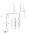
- FIG. 1 illustrates an image forming apparatus 102 as an electronic apparatus according to an embodiment of the present general inventive concept.
- FIG. 1 illustrates a laser printer as the image forming apparatus 102.
- the present general inventive concept is not limited thereto. It is possible that other types of printers can be used as the image forming apparatus 102. It is also possible that a portable and desktop electronic apparatus or home and office appliance can be used as the electronic apparatus.
- FIG. 1 illustrates a wired charging system
- the present general inventive concept can be applied to a wireless charging system, a near field charging system, etc., usable with the electronic apparatus.
- a power supply unit 202 (for example, Switching Mode Power Supply, SMPS) generates a system DC power of a plurality of different voltages, for example, 5V and 24V, such that the 5V and 24V system DC powers are applied to the controller 240, the image transfer unit 270, and other several units and components, respectively.
- the power supply unit 202 may also provide input commercial AC power to one or more corresponding units or components (for example, a fixing heater of the fusing unit 270).
- the paper feed unit 230 feeds a printing medium (a sheet of paper) loaded in a paper feeding cassette to the image transfer unit 250.
- the image transfer unit 250 forms a predetermined image according to an image signal, and transfers the formed image to the printing medium.
- the power supply unit 202a generates two system DC powers, for example, 5V and 24V, through an AC-DC conversion.
- the DC power of 5V is applied to a microprocessor, such as the controller 240 and a circuit element, and the DC power of 24V is applied to the fusing unit 170 or the like. It is possible that the system DC power of 5V or 24V generated from the power supply unit 202a may be selectively applied to other constituent units or elements (components) of the image forming apparatus 102.
- a discharge resistor R and a first switch or transistor for example, a bipolar transistor Q1 are connected in series between both terminals (first and second terminals or Live and Neutral terminals) of AC power input lines 202a and 202b, and a resistor 5R and a second switch or transistor, for example, a Metal Oxide Semiconductor Field Effect Transistor (MOSFET) Q2, connected in series are connected in parallel to the discharge resistor R and the bipolar transistor Q1.
- a base terminal of the bipolar transistor Q1 is connected between the resistor 5R and the MOSFET Q2, and a resistor R1 and a second capacitor, for example, a capacitor C1, are connected in parallel between a gate terminal and a neutral terminal of the MOSFET Q2.
- a diode D is connected between a node disposed between the resistor 5R and the MOSFET Q2 and a gate terminal of the MOSFET Q2.
- the discharge circuit 302a may minimize a power consumption caused by a discharge resistance generated in a plug-on mode, and is operated as follows.
- an amount of a power consumption generated under the turn-on state does not greatly reach 0.08W.
- the power loss generated by the turned-on MOSFET Q2 of the view (A) of FIG. 4 causes to turn off the bipolar transistor Q1, discharging through the discharge resistor R is not achieved, such that the amount of the power loss may be relatively very low as compared to an obtainable power loss restriction effect.
- a voltage charged in the X-Cap within a very short period of time needs to drop to a level such that the level of the voltage is not harmful to humans in the plug-off mode.
- the bipolar transistor Q1 is turned back on such that the X-Cap can be rapidly discharged.
- the plug-off mode charges charged in the capacitor C1 are rapidly discharged through the resistor R1, such that the MOSFET Q2 is turned off. If the MOSFET Q2 is turned off, a current flows in a base terminal of the bipolar transistor Q1 so that the bipolar transistor Q1 is turned on.
- charges of the X-Cap are rapidly discharged through the discharge resistor R and the turned-on bipolar transistor Q1.
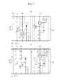
- FIG. 5 illustrates a discharge circuit 302b corresponding to the discharge circuit 302 of FIG. 3 according to an embodiment of the present general inventive concept.
- a view (A) of FIG. 5 illustrates a plug-on state
- a view (B) of FIG. 5 illustrates a plug-off state.
- one or more discharge resistors R and a bipolar transistor Q1 are connected in series between both terminals (Live, Neutral) of the AC power input line
- one or more resistors 5R and a bipolar transistor Q2 connected in series to each other are connected in parallel to the discharge resistors R and the bipolar transistor Q1.
- a base terminal of the bipolar transistor Q1 is connected between the resistor 5R and the bipolar transistor Q2, and a resistor R1 and a capacitor C1 (second capacitor) are connected in parallel between a base terminal and a neutral terminal of the bipolar transistor Q2.
- a diode D and a resistor 5R' are connected between a node disposed between the resistor 5R and the bipolar transistor Q2 and a base terminal of the bipolar transistor Q2.
- the discharge circuit 302a may minimize a power consumption caused by a discharge resistance generated in a plug-on mode, and is operated like the discharge circuit 302a of FIG. 4 so that a standby power loss is minimized.
- the discharge circuit 302b connects the one or more discharge resistors R in series as illustrated in FIG. 5 , such that a discharge resistance R with respect to disturbance such as external surge voltage can be increased.
- a universal general resistor instead of a special-purpose resistor can be usable to reduce production costs of the power supply unit 202.
- the resistor 5R is larger in size than the discharge resistor R such that a power loss of the resistor 5R can be reduced during a normal operation, and a turn-on power loss is reduced.
- signals are half-wave-rectified using the diode D, and the resistor 5R' is inserted to minimize the half-wave-rectified current, resulting in a current restriction.
- one or more discharge resistors R and a bipolar transistor Q1 are connected in series between both terminals (Live, Neutral) of the AC power line, and one or more resistors 5R and the MOSFET Q2 connected in series to each other are connected in parallel to the discharge resistors R and the bipolar transistor Q1.
- a base terminal of the bipolar transistor Q1 is connected between the resistor 5R and the bipolar transistor Q2, and a resistor R1 and a capacitor C1 (second capacitor) are connected in parallel between a gate terminal and a neutral terminal of the MOSFET Q2.
- a diode D and a resistor 5R' are connected between a node disposed between the resistor 5R and the MOSFET Q2 and a base terminal of the bipolar transistor Q2.
- the discharge circuit 302a may minimize a power consumption caused by a discharge resistance generated in a plug-on mode, and is operated like the discharge circuit 302a of FIG. 4 so that a standby power loss is minimized.
- FIG. 7 illustrates a discharge circuit 302d corresponding to the discharge circuit 302 of FIG. 3 according to an embodiment of the present general inventive concept.
- One or more different discharge circuits may be usable as the discharge circuit 302 of FIG. 3 as illustrated in FIG. 7 .
- the discharge circuit unit 302d includes a first discharge circuit 302e and a second discharge circuit 302f, and the first discharge circuit 302e and the second discharge circuit 302f are connected in parallel between both ends (Live, Neutral) of power lines 202a and 202b.
- the first discharge circuit 302d may have a structure same as or similar to that of the discharge circuit 302d of FIG. 6 .
- one or more discharge resistors R third discharge resistors
- a bipolar transistor Q1 third switch element
- one or more resistors 5R and the MOSFET Q2 are connected in parallel to the discharge resistors R and the bipolar transistor Q1.
- a base terminal of the bipolar transistor Q1 is connected between the resistor 5R and the bipolar transistor Q2, and the resistor R1 and the capacitor C1 are connected in parallel between the gate terminal and the neutral terminal of the MOSFET Q2.
- a diode D and the resistor 5R' are connected between a node disposed between the resistor 5R and the MOSFET Q2 and the base terminal of the bipolar transistor Q2.
- the second discharge circuit 302f has a structure same as or similar to that of the first discharge circuit 302f
- the first discharge circuit 302e is vertically inverted and connected between both ends (Live, Neutral) of the power lines 202a and 202b. That is, the first discharge circuit 302d is connected in a manner that it is discharged from the live terminal to the neutral terminal, but the second discharge circuit 302f is connected in a manner that it is discharged from the neutral terminal to the live terminal.
- One or more discharge resistors R (fourth discharge resistors) and the bipolar transistor Q1 (fourth switch element) are provided at the second discharge circuit 302f.
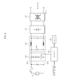
- FIG. 8 is a block diagram illustrating a control system having a power supply unit 202 and a controller 804 of the image forming apparatus 102 of FIG. 2 according to an embodiment of the present general inventive concept.
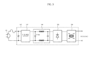
- the power supply unit 202 includes a discharge circuit unit 802, an EMI filter 304, a rectifier 306, and a transformer 308.
- the discharge circuit unit 802 may discharge the X-capacitor (X-Cap) of the EMI filter 304.
- the discharge circuit unit 803 is achieved by serially connecting the resistors R and the switch SW between both ends (Live, Neutral) of power lines 202a and 202b.
- the EMI filter 304 is used to remove various noise contained in the power cable 104 (See FIG.
- the DC voltage drop detection signal is generated when the DC voltage generated from a secondary portion of the transformer 308 is dropped to a predetermined level or less.
- the controller 804 recognizes a plug-off time point using the DC voltage drop detection signal, and discharges the X-Cap by turning on the switch SW of the discharge circuit 802. If a predetermined time (for example, one second) required to discharge the X-Cap elapses, the controller 804 turns off the switch SW of the discharge circuit unit 802.
Landscapes
- Engineering & Computer Science (AREA)
- Power Engineering (AREA)
- Business, Economics & Management (AREA)
- Emergency Management (AREA)
- Physics & Mathematics (AREA)
- General Physics & Mathematics (AREA)
- Electromagnetism (AREA)
- Radar, Positioning & Navigation (AREA)
- Automation & Control Theory (AREA)
- Direct Current Feeding And Distribution (AREA)
- Charge And Discharge Circuits For Batteries Or The Like (AREA)
- Control Or Security For Electrophotography (AREA)
Applications Claiming Priority (1)
| Application Number | Priority Date | Filing Date | Title |
|---|---|---|---|
| KR1020120095577A KR102048795B1 (ko) | 2012-08-30 | 2012-08-30 | 방전 회로, 방전 회로를 구비하는 화상 형성 장치 및 전력 공급부 |
Publications (3)
| Publication Number | Publication Date |
|---|---|
| EP2704281A2 true EP2704281A2 (de) | 2014-03-05 |
| EP2704281A3 EP2704281A3 (de) | 2017-04-05 |
| EP2704281B1 EP2704281B1 (de) | 2021-09-29 |
Family
ID=49036481
Family Applications (1)
| Application Number | Title | Priority Date | Filing Date |
|---|---|---|---|
| EP13182073.0A Not-in-force EP2704281B1 (de) | 2012-08-30 | 2013-08-28 | Entladeschaltung |
Country Status (4)
| Country | Link |
|---|---|
| US (1) | US9559527B2 (de) |
| EP (1) | EP2704281B1 (de) |
| KR (1) | KR102048795B1 (de) |
| CN (1) | CN103683903B (de) |
Cited By (1)
| Publication number | Priority date | Publication date | Assignee | Title |
|---|---|---|---|---|
| US10355600B1 (en) | 2018-10-29 | 2019-07-16 | Chicony Power Technology Co., Ltd. | Power converter |
Families Citing this family (15)
| Publication number | Priority date | Publication date | Assignee | Title |
|---|---|---|---|---|
| ITTO20110769A1 (it) * | 2011-08-12 | 2013-02-13 | Magneti Marelli Spa | Dispositivo e metodo di scarica per un condensatore in un impianto elettrico di potenza di un veicolo con trazione elettrica |
| US10345348B2 (en) | 2014-11-04 | 2019-07-09 | Stmicroelectronics S.R.L. | Detection circuit for an active discharge circuit of an X-capacitor, related active discharge circuit, integrated circuit and method |
| US9831761B2 (en) * | 2015-03-19 | 2017-11-28 | Chicony Power Technology Co., Ltd. | Speedy discharging circuit and power supply apparatus with speedy discharging circuit |
| CN104901297A (zh) * | 2015-06-26 | 2015-09-09 | 珠海格力电器股份有限公司 | 空调器的放电电路及其放电方法 |
| JP6611530B2 (ja) * | 2015-09-11 | 2019-11-27 | キヤノン株式会社 | 電力供給装置及び画像形成装置 |
| JP2017146260A (ja) * | 2016-02-19 | 2017-08-24 | 株式会社ケーヒン | 電圧検出装置 |
| US9985452B2 (en) * | 2016-03-03 | 2018-05-29 | GM Global Technology Operations LLC | Apparatus for discharging a high-voltage bus |
| CN106612067A (zh) * | 2017-01-06 | 2017-05-03 | 浙江凯耀照明股份有限公司 | 一种防过冲快速放电电路 |
| US11863062B2 (en) * | 2018-04-27 | 2024-01-02 | Raytheon Company | Capacitor discharge circuit |
| JP7119872B2 (ja) * | 2018-10-09 | 2022-08-17 | 株式会社デンソー | スイッチの駆動回路 |
| JP7629831B2 (ja) | 2021-09-17 | 2025-02-14 | シャープ株式会社 | 画像形成装置及び電気機器 |
| CN113793815B (zh) * | 2021-09-26 | 2024-04-26 | 杭州广立测试设备有限公司 | 一种宽电压范围高速多级放电电路、测试系统和放电方法 |
| DE102022120005A1 (de) * | 2022-08-09 | 2024-02-15 | Dr. Ing. H.C. F. Porsche Aktiengesellschaft | Verfahren und System zu einem Notfallbetrieb für einen modularen Multilevelkonverter |
| TWI822239B (zh) * | 2022-08-11 | 2023-11-11 | 致茂電子股份有限公司 | 雙向交流功率轉換裝置 |
| JP2024128615A (ja) * | 2023-03-10 | 2024-09-24 | 株式会社豊田自動織機 | 放電装置及び電動コンプレッサ |
Family Cites Families (16)
| Publication number | Priority date | Publication date | Assignee | Title |
|---|---|---|---|---|
| DE3545324A1 (de) * | 1985-12-20 | 1987-06-25 | Braun Ag | Elektronisches schaltnetzteil |
| JP3335136B2 (ja) * | 1998-04-28 | 2002-10-15 | 安致明 | 電力供給のフェードアウトスイッチング方法およびフェードアウトスイッチング装置 |
| JP2000184718A (ja) | 1998-12-10 | 2000-06-30 | Sharp Corp | スイッチング電源装置 |
| US7456611B2 (en) * | 2005-08-11 | 2008-11-25 | Semiconductor Components Industries, L.L.C. | Multi-current battery charger circuit and method therefor |
| US8829812B2 (en) * | 2008-04-04 | 2014-09-09 | Koninklijke Philips N.V. | Dimmable lighting system |
| US8212494B2 (en) * | 2008-04-04 | 2012-07-03 | Lemnis Lighting Patents Holding B.V. | Dimmer triggering circuit, dimmer system and dimmable device |
| JP5511225B2 (ja) * | 2009-06-03 | 2014-06-04 | ローム株式会社 | 昇圧型スイッチング電源装置 |
| DE102009034350A1 (de) * | 2009-07-23 | 2011-02-03 | Tridonicatco Gmbh & Co. Kg | Verfahren und Schaltung zur Leistungsfaktor-Korrektur |
| US8115457B2 (en) | 2009-07-31 | 2012-02-14 | Power Integrations, Inc. | Method and apparatus for implementing a power converter input terminal voltage discharge circuit |
| JP5094797B2 (ja) * | 2009-08-07 | 2012-12-12 | 日立オートモティブシステムズ株式会社 | 直流電源平滑用コンデンサーの放電回路 |
| KR20120016792A (ko) * | 2010-08-17 | 2012-02-27 | 삼성전자주식회사 | 디스플레이장치, 전원공급장치 및 그 전원공급방법 |
| JP5645700B2 (ja) * | 2011-02-16 | 2014-12-24 | キヤノン株式会社 | 放電回路、放電回路を有する電源及び画像形成装置 |
| JP2012186893A (ja) * | 2011-03-04 | 2012-09-27 | Honda Motor Co Ltd | 電動車両 |
| CN103219878B (zh) * | 2012-01-20 | 2016-06-01 | 台达电子企业管理(上海)有限公司 | 一种电容放电电路及功率变换器 |
| CN102594111A (zh) * | 2012-02-24 | 2012-07-18 | 中兴通讯股份有限公司 | 一种快速放电电路 |
| US9374858B2 (en) * | 2012-05-21 | 2016-06-21 | Cree, Inc. | Solid-state lighting apparatus and methods using switched energy storage |
-
2012
- 2012-08-30 KR KR1020120095577A patent/KR102048795B1/ko not_active Expired - Fee Related
-
2013
- 2013-08-28 EP EP13182073.0A patent/EP2704281B1/de not_active Not-in-force
- 2013-08-29 US US14/013,111 patent/US9559527B2/en not_active Expired - Fee Related
- 2013-08-30 CN CN201310390870.XA patent/CN103683903B/zh not_active Expired - Fee Related
Non-Patent Citations (1)
| Title |
|---|
| None |
Cited By (2)
| Publication number | Priority date | Publication date | Assignee | Title |
|---|---|---|---|---|
| US10355600B1 (en) | 2018-10-29 | 2019-07-16 | Chicony Power Technology Co., Ltd. | Power converter |
| TWI677173B (zh) * | 2018-10-29 | 2019-11-11 | 群光電能科技股份有限公司 | 電源轉換器 |
Also Published As
| Publication number | Publication date |
|---|---|
| EP2704281A3 (de) | 2017-04-05 |
| KR20140028698A (ko) | 2014-03-10 |
| CN103683903B (zh) | 2019-04-12 |
| EP2704281B1 (de) | 2021-09-29 |
| KR102048795B1 (ko) | 2019-11-26 |
| US20140062421A1 (en) | 2014-03-06 |
| CN103683903A (zh) | 2014-03-26 |
| US9559527B2 (en) | 2017-01-31 |
Similar Documents
| Publication | Publication Date | Title |
|---|---|---|
| EP2704281B1 (de) | Entladeschaltung | |
| KR101365602B1 (ko) | 전원 공급 장치 및 그를 포함하는 화상 형성 장치 | |
| JP5984999B2 (ja) | Dc/dcコンバータ、それを用いた電源装置 | |
| KR101487054B1 (ko) | 방전 회로 및 전원 | |
| JP3773512B2 (ja) | モーター電源供給装置 | |
| US9209621B2 (en) | Power supply system | |
| CN104104245B (zh) | 基于与负载的通信具有可选操作的电源 | |
| US9484798B2 (en) | Power control device and image forming apparatus including the same | |
| JP6039274B2 (ja) | Dc/dcコンバータおよびその制御回路、それを用いた電源装置、電源アダプタおよび電子機器 | |
| JP6319172B2 (ja) | 画像形成装置 | |
| US9715204B2 (en) | Discharge circuit unit and image forming apparatus having the same | |
| JP2006280135A (ja) | 電気機器、変換装置 | |
| JP2002095246A (ja) | 電源装置 | |
| JP2020188538A (ja) | 電源装置及び画像形成装置 | |
| JP5401045B2 (ja) | 電源回路 | |
| JP2003333747A (ja) | 電子機器の電源装置およびその制御方法 | |
| KR101328211B1 (ko) | 전력 절감 회로 및 이를 갖는 전원 공급 장치 | |
| JP5029034B2 (ja) | 電源装置 | |
| JP5108597B2 (ja) | 平滑コンデンサの放電回路を備えた電源基板 | |
| JP2013158211A (ja) | 放電回路及び放電回路を備えた電源 | |
| JP2010226933A (ja) | 保護回路、及び、電子機器 | |
| JP2010017001A (ja) | 多出力型スイッチング電源装置 | |
| JP2007282364A (ja) | 電力遮断監視回路 |
Legal Events
| Date | Code | Title | Description |
|---|---|---|---|
| AK | Designated contracting states |
Kind code of ref document: A2 Designated state(s): AL AT BE BG CH CY CZ DE DK EE ES FI FR GB GR HR HU IE IS IT LI LT LU LV MC MK MT NL NO PL PT RO RS SE SI SK SM TR |
|
| AX | Request for extension of the european patent |
Extension state: BA ME |
|
| PUAI | Public reference made under article 153(3) epc to a published international application that has entered the european phase |
Free format text: ORIGINAL CODE: 0009012 |
|
| PUAL | Search report despatched |
Free format text: ORIGINAL CODE: 0009013 |
|
| RAP1 | Party data changed (applicant data changed or rights of an application transferred) |
Owner name: S-PRINTING SOLUTION CO., LTD. |
|
| AK | Designated contracting states |
Kind code of ref document: A3 Designated state(s): AL AT BE BG CH CY CZ DE DK EE ES FI FR GB GR HR HU IE IS IT LI LT LU LV MC MK MT NL NO PL PT RO RS SE SI SK SM TR |
|
| AX | Request for extension of the european patent |
Extension state: BA ME |
|
| RIC1 | Information provided on ipc code assigned before grant |
Ipc: H02J 7/00 20060101ALI20170302BHEP Ipc: H02J 9/04 20060101ALI20170302BHEP Ipc: H02M 1/12 20060101ALI20170302BHEP Ipc: H02M 1/44 20070101ALN20170302BHEP Ipc: H02J 3/00 20060101AFI20170302BHEP Ipc: H02J 9/00 20060101ALI20170302BHEP Ipc: H02M 1/32 20070101ALN20170302BHEP Ipc: G03G 15/00 20060101ALN20170302BHEP |
|
| STAA | Information on the status of an ep patent application or granted ep patent |
Free format text: STATUS: REQUEST FOR EXAMINATION WAS MADE |
|
| 17P | Request for examination filed |
Effective date: 20170614 |
|
| RBV | Designated contracting states (corrected) |
Designated state(s): AL AT BE BG CH CY CZ DE DK EE ES FI FR GB GR HR HU IE IS IT LI LT LU LV MC MK MT NL NO PL PT RO RS SE SI SK SM TR |
|
| RAP1 | Party data changed (applicant data changed or rights of an application transferred) |
Owner name: HP PRINTING KOREA CO., LTD. |
|
| RAP1 | Party data changed (applicant data changed or rights of an application transferred) |
Owner name: HEWLETT-PACKARD DEVELOPMENT COMPANY, L.P. |
|
| STAA | Information on the status of an ep patent application or granted ep patent |
Free format text: STATUS: EXAMINATION IS IN PROGRESS |
|
| 17Q | First examination report despatched |
Effective date: 20200324 |
|
| GRAP | Despatch of communication of intention to grant a patent |
Free format text: ORIGINAL CODE: EPIDOSNIGR1 |
|
| STAA | Information on the status of an ep patent application or granted ep patent |
Free format text: STATUS: GRANT OF PATENT IS INTENDED |
|
| RIC1 | Information provided on ipc code assigned before grant |
Ipc: H02M 1/32 20070101ALN20210512BHEP Ipc: H02M 1/44 20070101ALN20210512BHEP Ipc: G03G 15/00 20060101ALN20210512BHEP Ipc: H02M 1/12 20060101ALI20210512BHEP Ipc: H02J 7/00 20060101ALI20210512BHEP Ipc: H02J 9/04 20060101ALI20210512BHEP Ipc: H02J 9/00 20060101ALI20210512BHEP Ipc: H02J 3/00 20060101AFI20210512BHEP |
|
| INTG | Intention to grant announced |
Effective date: 20210602 |
|
| GRAS | Grant fee paid |
Free format text: ORIGINAL CODE: EPIDOSNIGR3 |
|
| GRAA | (expected) grant |
Free format text: ORIGINAL CODE: 0009210 |
|
| STAA | Information on the status of an ep patent application or granted ep patent |
Free format text: STATUS: THE PATENT HAS BEEN GRANTED |
|
| AK | Designated contracting states |
Kind code of ref document: B1 Designated state(s): AL AT BE BG CH CY CZ DE DK EE ES FI FR GB GR HR HU IE IS IT LI LT LU LV MC MK MT NL NO PL PT RO RS SE SI SK SM TR |
|
| REG | Reference to a national code |
Ref country code: GB Ref legal event code: FG4D |
|
| REG | Reference to a national code |
Ref country code: DE Ref legal event code: R096 Ref document number: 602013079442 Country of ref document: DE |
|
| REG | Reference to a national code |
Ref country code: CH Ref legal event code: EP Ref country code: AT Ref legal event code: REF Ref document number: 1435054 Country of ref document: AT Kind code of ref document: T Effective date: 20211015 |
|
| REG | Reference to a national code |
Ref country code: IE Ref legal event code: FG4D |
|
| REG | Reference to a national code |
Ref country code: LT Ref legal event code: MG9D |
|
| PG25 | Lapsed in a contracting state [announced via postgrant information from national office to epo] |
Ref country code: BG Free format text: LAPSE BECAUSE OF FAILURE TO SUBMIT A TRANSLATION OF THE DESCRIPTION OR TO PAY THE FEE WITHIN THE PRESCRIBED TIME-LIMIT Effective date: 20211229 Ref country code: LT Free format text: LAPSE BECAUSE OF FAILURE TO SUBMIT A TRANSLATION OF THE DESCRIPTION OR TO PAY THE FEE WITHIN THE PRESCRIBED TIME-LIMIT Effective date: 20210929 Ref country code: RS Free format text: LAPSE BECAUSE OF FAILURE TO SUBMIT A TRANSLATION OF THE DESCRIPTION OR TO PAY THE FEE WITHIN THE PRESCRIBED TIME-LIMIT Effective date: 20210929 Ref country code: NO Free format text: LAPSE BECAUSE OF FAILURE TO SUBMIT A TRANSLATION OF THE DESCRIPTION OR TO PAY THE FEE WITHIN THE PRESCRIBED TIME-LIMIT Effective date: 20211229 Ref country code: FI Free format text: LAPSE BECAUSE OF FAILURE TO SUBMIT A TRANSLATION OF THE DESCRIPTION OR TO PAY THE FEE WITHIN THE PRESCRIBED TIME-LIMIT Effective date: 20210929 Ref country code: HR Free format text: LAPSE BECAUSE OF FAILURE TO SUBMIT A TRANSLATION OF THE DESCRIPTION OR TO PAY THE FEE WITHIN THE PRESCRIBED TIME-LIMIT Effective date: 20210929 Ref country code: SE Free format text: LAPSE BECAUSE OF FAILURE TO SUBMIT A TRANSLATION OF THE DESCRIPTION OR TO PAY THE FEE WITHIN THE PRESCRIBED TIME-LIMIT Effective date: 20210929 |
|
| REG | Reference to a national code |
Ref country code: NL Ref legal event code: MP Effective date: 20210929 |
|
| REG | Reference to a national code |
Ref country code: AT Ref legal event code: MK05 Ref document number: 1435054 Country of ref document: AT Kind code of ref document: T Effective date: 20210929 |
|
| PG25 | Lapsed in a contracting state [announced via postgrant information from national office to epo] |
Ref country code: LV Free format text: LAPSE BECAUSE OF FAILURE TO SUBMIT A TRANSLATION OF THE DESCRIPTION OR TO PAY THE FEE WITHIN THE PRESCRIBED TIME-LIMIT Effective date: 20210929 Ref country code: GR Free format text: LAPSE BECAUSE OF FAILURE TO SUBMIT A TRANSLATION OF THE DESCRIPTION OR TO PAY THE FEE WITHIN THE PRESCRIBED TIME-LIMIT Effective date: 20211230 |
|
| PG25 | Lapsed in a contracting state [announced via postgrant information from national office to epo] |
Ref country code: AT Free format text: LAPSE BECAUSE OF FAILURE TO SUBMIT A TRANSLATION OF THE DESCRIPTION OR TO PAY THE FEE WITHIN THE PRESCRIBED TIME-LIMIT Effective date: 20210929 |
|
| PG25 | Lapsed in a contracting state [announced via postgrant information from national office to epo] |
Ref country code: IS Free format text: LAPSE BECAUSE OF FAILURE TO SUBMIT A TRANSLATION OF THE DESCRIPTION OR TO PAY THE FEE WITHIN THE PRESCRIBED TIME-LIMIT Effective date: 20220129 Ref country code: SK Free format text: LAPSE BECAUSE OF FAILURE TO SUBMIT A TRANSLATION OF THE DESCRIPTION OR TO PAY THE FEE WITHIN THE PRESCRIBED TIME-LIMIT Effective date: 20210929 Ref country code: RO Free format text: LAPSE BECAUSE OF FAILURE TO SUBMIT A TRANSLATION OF THE DESCRIPTION OR TO PAY THE FEE WITHIN THE PRESCRIBED TIME-LIMIT Effective date: 20210929 Ref country code: PT Free format text: LAPSE BECAUSE OF FAILURE TO SUBMIT A TRANSLATION OF THE DESCRIPTION OR TO PAY THE FEE WITHIN THE PRESCRIBED TIME-LIMIT Effective date: 20220131 Ref country code: PL Free format text: LAPSE BECAUSE OF FAILURE TO SUBMIT A TRANSLATION OF THE DESCRIPTION OR TO PAY THE FEE WITHIN THE PRESCRIBED TIME-LIMIT Effective date: 20210929 Ref country code: NL Free format text: LAPSE BECAUSE OF FAILURE TO SUBMIT A TRANSLATION OF THE DESCRIPTION OR TO PAY THE FEE WITHIN THE PRESCRIBED TIME-LIMIT Effective date: 20210929 Ref country code: ES Free format text: LAPSE BECAUSE OF FAILURE TO SUBMIT A TRANSLATION OF THE DESCRIPTION OR TO PAY THE FEE WITHIN THE PRESCRIBED TIME-LIMIT Effective date: 20210929 Ref country code: EE Free format text: LAPSE BECAUSE OF FAILURE TO SUBMIT A TRANSLATION OF THE DESCRIPTION OR TO PAY THE FEE WITHIN THE PRESCRIBED TIME-LIMIT Effective date: 20210929 Ref country code: CZ Free format text: LAPSE BECAUSE OF FAILURE TO SUBMIT A TRANSLATION OF THE DESCRIPTION OR TO PAY THE FEE WITHIN THE PRESCRIBED TIME-LIMIT Effective date: 20210929 Ref country code: AL Free format text: LAPSE BECAUSE OF FAILURE TO SUBMIT A TRANSLATION OF THE DESCRIPTION OR TO PAY THE FEE WITHIN THE PRESCRIBED TIME-LIMIT Effective date: 20210929 |
|
| REG | Reference to a national code |
Ref country code: DE Ref legal event code: R097 Ref document number: 602013079442 Country of ref document: DE |
|
| PG25 | Lapsed in a contracting state [announced via postgrant information from national office to epo] |
Ref country code: DK Free format text: LAPSE BECAUSE OF FAILURE TO SUBMIT A TRANSLATION OF THE DESCRIPTION OR TO PAY THE FEE WITHIN THE PRESCRIBED TIME-LIMIT Effective date: 20210929 |
|
| PLBE | No opposition filed within time limit |
Free format text: ORIGINAL CODE: 0009261 |
|
| STAA | Information on the status of an ep patent application or granted ep patent |
Free format text: STATUS: NO OPPOSITION FILED WITHIN TIME LIMIT |
|
| 26N | No opposition filed |
Effective date: 20220630 |
|
| PGFP | Annual fee paid to national office [announced via postgrant information from national office to epo] |
Ref country code: GB Payment date: 20220721 Year of fee payment: 10 Ref country code: DE Payment date: 20220616 Year of fee payment: 10 |
|
| PG25 | Lapsed in a contracting state [announced via postgrant information from national office to epo] |
Ref country code: SI Free format text: LAPSE BECAUSE OF FAILURE TO SUBMIT A TRANSLATION OF THE DESCRIPTION OR TO PAY THE FEE WITHIN THE PRESCRIBED TIME-LIMIT Effective date: 20210929 |
|
| PGFP | Annual fee paid to national office [announced via postgrant information from national office to epo] |
Ref country code: FR Payment date: 20220721 Year of fee payment: 10 |
|
| PG25 | Lapsed in a contracting state [announced via postgrant information from national office to epo] |
Ref country code: IT Free format text: LAPSE BECAUSE OF FAILURE TO SUBMIT A TRANSLATION OF THE DESCRIPTION OR TO PAY THE FEE WITHIN THE PRESCRIBED TIME-LIMIT Effective date: 20210929 |
|
| PG25 | Lapsed in a contracting state [announced via postgrant information from national office to epo] |
Ref country code: MC Free format text: LAPSE BECAUSE OF FAILURE TO SUBMIT A TRANSLATION OF THE DESCRIPTION OR TO PAY THE FEE WITHIN THE PRESCRIBED TIME-LIMIT Effective date: 20210929 |
|
| REG | Reference to a national code |
Ref country code: CH Ref legal event code: PL |
|
| PG25 | Lapsed in a contracting state [announced via postgrant information from national office to epo] |
Ref country code: LU Free format text: LAPSE BECAUSE OF NON-PAYMENT OF DUE FEES Effective date: 20220828 Ref country code: LI Free format text: LAPSE BECAUSE OF NON-PAYMENT OF DUE FEES Effective date: 20220831 Ref country code: CH Free format text: LAPSE BECAUSE OF NON-PAYMENT OF DUE FEES Effective date: 20220831 |
|
| REG | Reference to a national code |
Ref country code: BE Ref legal event code: MM Effective date: 20220831 |
|
| PG25 | Lapsed in a contracting state [announced via postgrant information from national office to epo] |
Ref country code: IE Free format text: LAPSE BECAUSE OF NON-PAYMENT OF DUE FEES Effective date: 20220828 |
|
| PG25 | Lapsed in a contracting state [announced via postgrant information from national office to epo] |
Ref country code: BE Free format text: LAPSE BECAUSE OF NON-PAYMENT OF DUE FEES Effective date: 20220831 |
|
| REG | Reference to a national code |
Ref country code: DE Ref legal event code: R119 Ref document number: 602013079442 Country of ref document: DE |
|
| PG25 | Lapsed in a contracting state [announced via postgrant information from national office to epo] |
Ref country code: HU Free format text: LAPSE BECAUSE OF FAILURE TO SUBMIT A TRANSLATION OF THE DESCRIPTION OR TO PAY THE FEE WITHIN THE PRESCRIBED TIME-LIMIT; INVALID AB INITIO Effective date: 20130828 |
|
| GBPC | Gb: european patent ceased through non-payment of renewal fee |
Effective date: 20230828 |
|
| PG25 | Lapsed in a contracting state [announced via postgrant information from national office to epo] |
Ref country code: SM Free format text: LAPSE BECAUSE OF FAILURE TO SUBMIT A TRANSLATION OF THE DESCRIPTION OR TO PAY THE FEE WITHIN THE PRESCRIBED TIME-LIMIT Effective date: 20210929 Ref country code: CY Free format text: LAPSE BECAUSE OF FAILURE TO SUBMIT A TRANSLATION OF THE DESCRIPTION OR TO PAY THE FEE WITHIN THE PRESCRIBED TIME-LIMIT Effective date: 20210929 |
|
| PG25 | Lapsed in a contracting state [announced via postgrant information from national office to epo] |
Ref country code: MK Free format text: LAPSE BECAUSE OF FAILURE TO SUBMIT A TRANSLATION OF THE DESCRIPTION OR TO PAY THE FEE WITHIN THE PRESCRIBED TIME-LIMIT Effective date: 20210929 |
|
| PG25 | Lapsed in a contracting state [announced via postgrant information from national office to epo] |
Ref country code: TR Free format text: LAPSE BECAUSE OF FAILURE TO SUBMIT A TRANSLATION OF THE DESCRIPTION OR TO PAY THE FEE WITHIN THE PRESCRIBED TIME-LIMIT Effective date: 20210929 |
|
| PG25 | Lapsed in a contracting state [announced via postgrant information from national office to epo] |
Ref country code: GB Free format text: LAPSE BECAUSE OF NON-PAYMENT OF DUE FEES Effective date: 20230828 |
|
| PG25 | Lapsed in a contracting state [announced via postgrant information from national office to epo] |
Ref country code: GB Free format text: LAPSE BECAUSE OF NON-PAYMENT OF DUE FEES Effective date: 20230828 Ref country code: FR Free format text: LAPSE BECAUSE OF NON-PAYMENT OF DUE FEES Effective date: 20230831 Ref country code: DE Free format text: LAPSE BECAUSE OF NON-PAYMENT OF DUE FEES Effective date: 20240301 |
|
| PG25 | Lapsed in a contracting state [announced via postgrant information from national office to epo] |
Ref country code: MT Free format text: LAPSE BECAUSE OF FAILURE TO SUBMIT A TRANSLATION OF THE DESCRIPTION OR TO PAY THE FEE WITHIN THE PRESCRIBED TIME-LIMIT Effective date: 20210929 |