EP2704321B1 - Adaptives gestuftes Verstärkersystem und -verfahren - Google Patents
Adaptives gestuftes Verstärkersystem und -verfahren Download PDFInfo
- Publication number
- EP2704321B1 EP2704321B1 EP12290284.4A EP12290284A EP2704321B1 EP 2704321 B1 EP2704321 B1 EP 2704321B1 EP 12290284 A EP12290284 A EP 12290284A EP 2704321 B1 EP2704321 B1 EP 2704321B1
- Authority
- EP
- European Patent Office
- Prior art keywords
- gain
- amplifier
- steps
- control
- controlling
- Prior art date
- Legal status (The legal status is an assumption and is not a legal conclusion. Google has not performed a legal analysis and makes no representation as to the accuracy of the status listed.)
- Active
Links
Images


Classifications
-
- H—ELECTRICITY
- H03—ELECTRONIC CIRCUITRY
- H03G—CONTROL OF AMPLIFICATION
- H03G3/00—Gain control in amplifiers or frequency changers
- H03G3/20—Automatic control
- H03G3/30—Automatic control in amplifiers having semiconductor devices
- H03G3/3052—Automatic control in amplifiers having semiconductor devices in bandpass amplifiers (H.F. or I.F.) or in frequency-changers used in a (super)heterodyne receiver
- H03G3/3068—Circuits generating control signals for both R.F. and I.F. stages
-
- H—ELECTRICITY
- H04—ELECTRIC COMMUNICATION TECHNIQUE
- H04B—TRANSMISSION
- H04B1/00—Details of transmission systems, not covered by a single one of groups H04B3/00 - H04B13/00; Details of transmission systems not characterised by the medium used for transmission
- H04B1/06—Receivers
- H04B1/10—Means associated with receiver for limiting or suppressing noise or interference
-
- H—ELECTRICITY
- H03—ELECTRONIC CIRCUITRY
- H03G—CONTROL OF AMPLIFICATION
- H03G1/00—Details of arrangements for controlling amplification
- H03G1/0005—Circuits characterised by the type of controlling devices operated by a controlling current or voltage signal
-
- H—ELECTRICITY
- H03—ELECTRONIC CIRCUITRY
- H03G—CONTROL OF AMPLIFICATION
- H03G3/00—Gain control in amplifiers or frequency changers
- H03G3/20—Automatic control
- H03G3/30—Automatic control in amplifiers having semiconductor devices
- H03G3/3052—Automatic control in amplifiers having semiconductor devices in bandpass amplifiers (H.F. or I.F.) or in frequency-changers used in a (super)heterodyne receiver
- H03G3/3078—Circuits generating control signals for digitally modulated signals
Definitions
- This invention relates to variable gain amplifiers.
- Broadband receivers such as silicon tuners for television reception usually have RF variable gain amplifiers, implementing an automatic gain control (AGC).
- AGC automatic gain control
- Stepped AGC amplifier implementations provide, generally, less noise and distortion because the variable gain levels are implemented using switching components (resistors or reactive components) instead of relying on analogue transconductance changes.
- gain step killer systems which allow stepped AGC control but without the noise problems.
- Figure 1 shows a known gain step killer system, for example as disclosed in US 2010/0231801 and US 2010/0130153 .
- the system comprises a stepped gain amplifier 10, a mixer 12 for frequency down-converting the RF signal and a "gain step killer" unit 14.
- a demodulator When used with a receiver, a demodulator will also be provided, not shown in Figure 1 .
- the mixer can for example provide a translation in frequency from the RF frequency to an intermediate frequency.
- Figure 2 shows the RF amplifier gain step, with a step increase in gain at a particular point in time.
- FIG 3 shows an IF amplifier gain counter-step followed by very small gain steps.
- the large gain step is in the opposite direction to the gain step in Figure 2 and is followed by a series of smaller steps ramping back to the original level. This is the so-called “gain step killer” principle.
- Figure 4 shows the overall receiver gain with the RF amplifier response of Figure 2 and the IF amplifier response of Figure 3 . This approach avoids sudden changes in power level, which can give rise to image flicker or audio noise.
- Figure 5 shows a real RF amplifier gain step variation with frequency.
- the RF amplifier can be considered to have several different gain settings.
- Figure 5 shows two different gain settings for an RF amplifier versus frequency.
- the depicted gain transfer functions correspond to two consecutive gain settings for the RF amplifier.
- the targeted gain step for these two consecutive gain settings of the RF amplifier is 3 dB.
- the real design has some imperfections (parasitic capacitance of the components and layout). Due to these imperfections the targeted gain step is not constant and can vary from 3 dB to only 1.5 dB over the frequency range as shown in Figure 5 .
- the RF amplifier gain step is 1.5 dB.
- Figure 6 shows a real receiver output level with gain step compensation errors.
- the gain step of the IF amplifier can be assumed to be constant, because the IF frequency bandwidth is smaller than the RF frequency bandwidth. In this case, the RF gain step is not perfectly compensated by the IF gain step as shown in Figure 6 , and some errors appear. There is a step compensation error 20 (because the height of the RF gain step of Figure 2 and the IF gain step of Figure 3 are not the same). This leads to a residual step 22, so that the desired gain change has not been implemented. Thus, although the AGC has in theory implemented a 3dB gain step, at the particular frequency the RF amplifier gain has not achieved the desired gain increase.
- an RF amplifier system comprising:
- the invention uses a stepped gain amplifier to enable high dynamic range and to enable high signal-to-noise ratio of reception when used in a receiver. Compensation for gain step errors is carried out later in the receiver chain with a second amplifier, which can be a so-called "gain step killer" system.
- the second amplifier is used not only as a gain step killer system, but it is also used to compensate for frequency dependent errors in the gain applied by the AGC loop of the first amplifier. In this way, the step size (of the first amplifier) is dynamically compensated by the second amplifier.
- the controller is preferably adapted to control the gain of the first amplifier during a channel changing time period.
- a set of measurements of actual gain are used to enable control of the gain applied by the second amplifier. These measurements are taken during channel change so that the measurements do not affect the signal provided to the user.
- the controller preferably is adapted to control the gain of the second amplifier using the gain setting values stored in the memory during channel reception. This then provides compensation for step errors during channel reception.
- the controller is preferably adapted to control the gain of the second amplifier to provide a gain step killer function during channel reception if AGC gain changes of the first amplifier are applied.
- the normal gain step killer function can be implemented by the second amplifier, in addition to the function of compensating for errors in the gain step applied by the first amplifier.
- the first set of gain steps are preferably spaced further apart than the second set of gain steps.
- the first set of gain steps are spaced further apart by more than 2dB and the second set of gain steps are spaced apart by less than 0.5dB
- the invention can be used in a broadband receiver comprising a channel tuner and the RF amplifier system of the invention. Gain setting values for a plurality of frequencies are then stored in the memory.
- the invention provides a method of setting the gain of an RF amplifier system, comprising:
- the invention provides an adaptive stepped gain amplifier, for example for use in broadband receivers.
- the step size is dynamically compensated (for each received frequency) to cope with step error caused by frequency dependence of the amplifier performance.
- a calibration can be carried out, using a test calibration signal in the form of an embedded test tone.
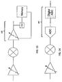
- Figure 7 shows such a calibration signal 30 routed to the input of the system of Figure 1 .
- the calibration signal is injected directly at the input, which is a problem in case of cable TV reception for example, because in case of cable reception it is not allowed to inject a signal in the cable. In this case a test tone cannot be injected directly at the antenna.
- test tone used for calibration signal 30 can be injected after a first amplification stage 32 as shown in Figure 8 .
- This amplification stage 32 cannot be calibrated so the use of a fixed gain amplifier is required.
- the invention relates to a calibration approach to overcome the problem of gain step compensation error and residual step error. It is desirable to avoid the use of a calibration signal injected at the input, since this is not possible in the case of cable TV reception, for example
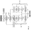
- FIG. 9 shows in schematic form the system of the invention.
- the system comprises an RF amplifier 90 which implements AGC, with gain steps. These gain steps have a first step size, for example 3dB.
- a mixer 92 translates to intermediate frequency.
- An IF amplifier system 94 compensates for the RF amplifier gain steps.
- the IF amplifier 94 can operate in the analog or digital domain (after Analog-to-Digital conversion).
- the IF amplifier also applies gain steps, but with smaller step size, for example 0.2 dB for digital TV.
- the gain setting of the IF amplifier can be used to fine tune the overall gain of the system, and this can be on a per-channel basis or for a group of channels present in the IF signal.
- the IF amplifier is controlled by a controller 96 which can be in the form of a digital state machine including an algorithm to measure and store dynamically, in an embedded or external memory 98, the RF amplifier gain steps at channel/frequency selection and/or at initialization.
- the gain steps of the IF amplifier follow a ramp for example as shown in Figure 4 .
- a signal strength indicator 99 is provided (although shown as a separate unit, this can be part of the controller 96), and is used to measure the impairments between the RF and IF domain.
- the gain of the RF amplifier 90 is set by an AGC loop. It can for example comprise a wideband RF detector sensing the output of the amplifier 90 and a digital decoder which sets the gain of the amplifier 90.
- the memory is used to store the exact value of the gain steps of the RF amplifier 90, for each channel (because the gain steps vary with frequency, thus are different from one channel to another).
- the signal strength indicator 99 measures a power level, for example the RSSI.
- the system aims to optimise the residual gain step as shown in Figure 6 by selecting the gain step that gives the optimum RSSI.
- the measurement of the RF amplifier gain steps follows a pattern as explained below with reference to Figures 10 and 11 .
- the controller 96 takes the control of the RF amplifier gain and the the AGC loop is turned OFF, so that the gain steps can be measured. After the calibration phase the AGC loop is ON again.
- the stored gain steps can then be used by the IF amplifier to compensate accurately for the RF amplifier gain steps
- Figures 10 and 11 show the amplifier gain of the RF amplifier 90 as a function of time.
- the RF amplifier gain can vary from “Min gain” to “Max gain” with gain steps. These gain steps have some frequency variation as shown in Fig 5 .
- the invention is implemented by forcing the gain of the RF amplifier at a set of values and measuring and storing the corresponding gain steps.
- the gain steps shown in Figure 10 are all the larger gain steps of the RF amplifier, for example 3dB.
- the gain of the RF amplifier is forced around the final value "new channel gain”. This measurement period includes a slope up in the gain curve from 6 steps below the final value to 6 steps above the final value.
- the gain steps applied to the RF amplifier are fast enough to be included in the channel change procedure (which has a duration shown as "max available time” in Figure 10 ) so that no perturbation is seen on the screen.
- Figure 11 shows the same approach but when the channel gain is increasing up to close to the maximum gain (left image) and when the channel gain is decreasing down to close to the minimum gain (right image). In these cases, it is not possible to provide an equal number of smaller gain steps above and below the new channel gain value because of the maximum and minimum levels.
- the RF gain steps are measured near the new channel selection gain settings for example in order to compensate for daily change.
- the stored gain steps are then used subsequently to compensate for the RF amplifier gain steps during reception.
- the invention can be understood by considering three different time periods during TV reception. Note that TV reception is taken as an example of the invention, the concept of the invention can be extended to the reception of other standards.
- the end user During reception of a channel, the end user is looking at the TV and no perturbation is allowed to keep a high quality image and sound. In this case, only very small gain steps are acceptable (for example 0.2 dB). At the RF side of the receiver, it is difficult to implement 0.2 dB steps, and a 3 dB step amplifier is instead implemented. If the end user is looking at the TV for a very long time, some changes in the level of the received spectrum can be encountered (termed “daily change").
- the gain of the amplifiers in the receiver has to be change to keep a good noise/linearity tradeoff.
- large gain steps of 3 dB are to be avoided during reception of a channel to avoid image or noise degradation.
- 3 dB gain steps are implemented in the RF amplifier to keep a good noise/linearity tradeoff, and the large gain steps will be compensated by the 0.2 dB gain steps in the IF amplifier, so that the demodulator sees only 0.2 dB gain steps coming from the front end.
- This is the known gain step killer approach.
- the problem is that RF gain steps are not well controlled and can vary with frequency. Therefore by measuring and storing the gain steps of the RF amplifier for a given frequency, the IF amplifier can be controlled to provide a different gain step (2.5 dB or 3.8 dB for example instead of 3 dB).
- the gain steps of the RF amplifier are measured during channel change as shown in Figures 10 and 11 .
- gain steps are stored in the memory they can be used for accurate gain step compensation during reception.
- the system thus uses the gain step killer unit to eliminate abrupt steps during normal channel reception as is known, but the size of the total gain step applied by the gain step killer system is then variable and dependent on the frequency dependency of the RF amplifier.
- Figure 12 shows an example of the control algorithm.
- the following definitions are used:
- the algorithm essentially provides the operation shown in Figures 10 and 11 .
- the two tests 120, 122 determined if there is room above and below the target gain level for half the number of steps. If there is, the algorithm implements gain control as in Figure 10 , and if there is not, it implements one of the gain control functions of Figure 11 .
- Branch 124 decreases the gain in steps from the maximum gain until the required number of steps has been carried out (left part of Figure 11 ).
- Brach 126 increases the gain in steps from the minimum gain (right part of Figure 11 ) or from the target gain less half the number of steps ( Figure 10 ) until the required number of steps has been carried out.
- the system performs a measure of the gain step when a channel change is implemented.
- the gain of the RF amplifier will vary if the level of the new selected channel/frequency is different from the level of the previous channel.
- intermediate gain steps can be measured by the signal strength indicator (or digital AGC) and stored in the memory.
- a Flash memory can for example be used to store multiple possible gain steps after several channel changes have taken place.
- the memory is in this way built up over time.
- the intermediate steps are measured near the new channel selection gain settings in order to compensate for daily change.
- the RF amplifier is automatically programmed to the final gain thanks to the AGC loop and then is adjusted back and forth rapidly across the dynamic range of the RF amplifier gain to measure the gain step inaccuracy.
- the gain function has for a small period of time an overshoot in the gain setting which then comes back to the final setting.
- the stored gain steps are used subsequently to compensate for the RF amplifier gain steps during reception.
- the number of steps to be stored can be adapted to save memory capability.
- the gain of the RF amplifier is measured during a channel change procedure.
- the gain of the RF amplifier is changed because of a different power level between previous and new channels.
- the RF amplifier passes through several gain steps before reaching its targetted gain. The goal is to measure as many gain steps of the RF amplifier as possible and store the information in the memory so that it can be used at another channel change.
- the IF amplifier will be controlled by the system to avoid as much as possible the residual gain step as shown in Figure 6 .
- Figures 10 and 11 show the gain of the RF amplifier only, rather than the gain of the whole system.
- the invention provides a suitable correction after the RF AGC. After the correction, the invention enables ideal gain variations to be provided as shown in Figures 2 to 4 for all channels to be received, thus for all the frequencies of interest.
- the invention aims to characterise all gains steps of the RF amplifier for each channel in a memory. In this way, for each RF amplifier gain step, and for each channel (thus for each frequency), the IF amplifier can compensate for the RF amplifier gain steps with a very good accuracy as shown in Figures 2 to 4 , or at least with a very small residual step error as explained with reference to Figure 6 .
- the invention does not need any calibration signal generator. Calibration of the gain steps of the first amplifier is possible and the gain steps of the first amplifier are measured in real time.
- the invention can be implemented in different ways depending on RF and IF partitioning.
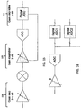
- Figure 13 shows an implementation with an IF analog gain step killer 130.
- the compensation of the RF gain steps is made with an IF amplifier in the analog domain and using a signal strength indicator for measurement purposes.
- the controller is not shown, and this version corresponds to Figure 9 .
- Figure 14 shows an implementation with an IF digital gain step killer 140.
- the IF signal is sampled and digitized.
- the digital AGC implementation can be used for measurement and also the compensation for the gain step impairments.
- Figure 15 shows an implementation with both IF analog and digital gain step killer. This has compensation in the analog domain.
- the gain step compensation is performed by both analog and digital AGCs.
- the RF amplifier is shown as 150.
- the Analog AGC 151 is considered to be fixed with 3 dB compensation in conventional manner.
- the digital AGC 152 is used to compensate for errors in the gain steps of the RF amplifier 150. If the gain step of the RF amplifier 150 is not 3 dB as targeted but only (3 - x) dB as shown, then the analog amplifier will Implement a 3 dB gain step, and the digital amplifier will implement an "x dB" gain step.
- the very small steps can be implemented in the analog amplifier or in the digital amplifier. Implementation in the digital amplifier 152 is preferred as it is easier to implement small steps in the digital domain than in analog domain.
- the invention can be applied in multiple stream receivers.
- the RF amplification covers a full spectrum comprising distinct channels or frequencies.
- Figure 16 shows how the invention can be used with a wide band full spectrum receiver. This is a "Software Radio" implementation with multiple channel reception realised in the digital domain where AGC1 and AGC2 compensate for the gain step inaccuracy of the RF amplifier allowing compensation of different values of steps due to frequency dependence.
Landscapes
- Engineering & Computer Science (AREA)
- Computer Networks & Wireless Communication (AREA)
- Signal Processing (AREA)
- Circuits Of Receivers In General (AREA)
Claims (14)
- Ein RF Verstärkersystem aufweisend:einen ersten Verstärker (90), welcher eine automatische Verstärkungsfaktorsteuerung hat, welche steuerbar ist, um den Verstärkungsfaktor des ersten Verstärkers in einem ersten Satz von Verstärkungsfaktorschritten zu variieren und zum Bereitstellen eines Ziel-Verstärkungsfaktorwerts;einen zweiten Verstärker (94), welcher einen Verstärkungsfaktor hat, welcher in einem zweiten Satz von Verstärkungsfaktorschritten steuerbar ist;einen Controller (96), welcher an den ersten Verstärker und an den zweiten Verstärker gekoppelt ist, wobei der Controller eingerichtet ist zum
Steuern des Verstärkungsfaktors von dem ersten Verstärker (90) anstelle der automatischen Verstärkungssteuerung während einer Kalibrationsphase,
und zum Anpassen des Verstärkungsfaktors von dem ersten Verstärker (90) in Schritten während der Kalibrationsphase, so dass der Verstärkungsfaktor von dem Verstärkersystem in einem Bereich variiert, welcher den Ziel-Verstärkungsfaktorwert enthält,
um dadurch den Verstärkungsfaktor von dem ersten Verstärker (90) zu steuern, so dass das Verstärkersystem einen Verstärkungsfaktor aufweist, welcher an jeder Seite von dem Ziel-Verstärkungsfaktorwert variiert;eine Messeinheit (99) zum Messen einer Signalstärke an einem Ausgang von dem System bei verschiedenen Verstärkungsfaktor Einstellungen von dem ersten Verstärker und bei verschiedenen RF Frequenzen; undeinen Speicher zum Speichern von Verstärkungsfaktorschritten, welche von den Messungen abgeleitet sind, welche mittels der Messeinheit (99) für eine Mehrzahl von verschiedenen RF Frequenzen genommen sind;wobei der Controller ferner eingerichtet ist zum Steuern des Verstärkungsfaktors von dem zweiten Verstärker basierend auf den Verstärkungsfaktorschritten von dem ersten Verstärker, welche in dem Speicher gespeichert sind. - Ein System gemäß Anspruch 1, wobei der Controller adaptiert ist zum Steuern des Verstärkungsfaktors von dem ersten Verstärker (90) während einer Kanal-ändernden Zeitperiode.
- Ein System gemäß einem beliebigen vorhergehenden Anspruch, wobei der Controller adaptiert ist zum Steuern des Verstärkungsfaktors von dem zweiten Verstärker, um eine Verstärkungsfaktorschritt Beende-Funktion während eines Kanal-Empfangs bereitzustellen, wenn eine automatische Verstärkungssteuerung Änderungen von dem ersten Verstärker angewendet sind.
- Ein System gemäß einem beliebigen vorhergehenden Anspruch, wobei die Verstärkungsfaktorschritte des ersten Satzes weiter voneinander entfernt sind als die Verstärkungsfaktorschritte des zweiten Satzes.
- Ein System gemäß einem beliebigen vorhergehenden Anspruch, wobei die Verstärkungsfaktorschritte des ersten Satzes mehr als 2 dB voneinander entfernt sind und die Verstärkungsfaktorschritte des zweiten Satzes weniger als 0.5 dB voneinander entfernt sind.
- Ein Breitbandempfänger aufweisend einen Kanal-Abstimmer und ein RF Verstärkersystem gemäß einem beliebigen vorhergehenden Anspruch.
- Ein Empfänger gemäß Anspruch 6, wobei Verstärkungsfaktor-einstellende Werte für eine Mehrzahl von Kanälen in dem Speicher gespeichert sind.
- Ein Verfahren zum Einstellen des Verstärkungsfaktors von einem RF Verstärkersystem, aufweisend:Steuern eines ersten Verstärkers (90), welcher eine automatische Verstärkungssteuerung hat und in einem ersten Satz von Verstärkungsfaktorschritten steuerbar ist, um einen Ziel-Verstärkungsfaktorwert bereitzustellen;Steuern des Verstärkungsfaktors von dem ersten Verstärker (90) während einer Kalibrationsphase, in welcher die automatische Verstärkungsfaktorsteuerung daran gehindert wird, eine Reihe von Verstärkungsfaktorschritten bereitzustellen, so dass der Verstärkungsfaktor des Verstärkersystems innerhalb eines Bereichs variiert, welcher den Ziel-Verstärkungsfaktorwert enthält, um dadurch den Verstärkungsfaktor von dem ersten Verstärker (90) zu steuern, so dass das Verstärkersystem einen Verstärkungsfaktor hat, welcher an jeder Seite von dem Ziel-Verstärkungsfaktorwert variiert;Messen einer Signalstärke an einem Ausgang von dem System bei verschiedenen Verstärkungsfaktor-Einstellungen von dem ersten Verstärker und bei verschiedenen RF Frequenzen, um dadurch gemessene Verstärkungsfaktorschritte abzuleiten;Speichern der gemessenen Verstärkungsfaktorschritte für verschiedene Verstärkungsfaktor-einstellende Werte, welche von den Messungen abgeleitet sind, welche mittels der Messeinheit (99) für eine Mehrzahl von verschiedenen RF Frequenzen genommen wurden;Steuern eines Verstärkungsfaktors von einem zweiten Verstärker basierend auf den gespeicherten Verstärkungsfaktorschritten von dem ersten Verstärker.
- Ein Verfahren gemäß Anspruch 8, aufweisend ein Steuern des Verstärkungsfaktors von dem ersten Verstärker (90) während einer Kanal-ändernden Zeitperiode.
- Ein Verfahren gemäß Anspruch 8 oder 9, aufweisend ein Steuern des Verstärkungsfaktors von dem zweiten Verstärker unter Verwenden der Verstärkungsfaktor einstellenden Werte, welche in dem Speicher während einem Kanal-Empfang gespeichert werden.
- Ein Verfahren gemäß einem beliebigen von den Ansprüchen 8 bis 10, aufweisend ein Steuern des Verstärkungsfaktors von dem zweiten Verstärker, um eine Verstärkungsfaktorschritt Beende-Funktion während dem Kanal-Empfang bereitzustellen, wenn Verstärkungsfaktor Änderungen der automatischen Verstärkungssteuerung von dem ersten Verstärker angewendet werden.
- Ein Verfahren gemäß einem beliebigen von den Ansprüchen 8 bis 11, wobei die Verstärkungsfaktorschritte des ersten Satzes weiter voneinander entfernt sind als die Verstärkungsfaktorschritte des zweiten Satzes.
- Ein Verfahren gemäß einem beliebigen von den Ansprüchen 8 bis 12, wobei die Verstärkungsfaktorschritte des ersten Satzes weiter als 2 dB voneinander entfernt sind und die Verstärkungsfaktorschritte des zweiten Satzes weniger als 0,5 dB voneinander entfernt sind.
- Ein Verfahren gemäß einem beliebigen von den Ansprüchen 8 bis 13, zum Einstellen des Verstärkungsfaktors von einem RF Verstärker von einem RF Empfänger.
Priority Applications (2)
| Application Number | Priority Date | Filing Date | Title |
|---|---|---|---|
| EP12290284.4A EP2704321B1 (de) | 2012-08-28 | 2012-08-28 | Adaptives gestuftes Verstärkersystem und -verfahren |
| US13/965,408 US8913975B2 (en) | 2012-08-28 | 2013-08-13 | Adaptive stepped gain amplifier system and method |
Applications Claiming Priority (1)
| Application Number | Priority Date | Filing Date | Title |
|---|---|---|---|
| EP12290284.4A EP2704321B1 (de) | 2012-08-28 | 2012-08-28 | Adaptives gestuftes Verstärkersystem und -verfahren |
Publications (2)
| Publication Number | Publication Date |
|---|---|
| EP2704321A1 EP2704321A1 (de) | 2014-03-05 |
| EP2704321B1 true EP2704321B1 (de) | 2016-04-06 |
Family
ID=47074661
Family Applications (1)
| Application Number | Title | Priority Date | Filing Date |
|---|---|---|---|
| EP12290284.4A Active EP2704321B1 (de) | 2012-08-28 | 2012-08-28 | Adaptives gestuftes Verstärkersystem und -verfahren |
Country Status (2)
| Country | Link |
|---|---|
| US (1) | US8913975B2 (de) |
| EP (1) | EP2704321B1 (de) |
Families Citing this family (6)
| Publication number | Priority date | Publication date | Assignee | Title |
|---|---|---|---|---|
| US8324943B1 (en) * | 2009-01-28 | 2012-12-04 | Cirrus Logic, Inc. | High voltage linear amplifier driving heavy capacitive loads with reduced power dissipation |
| KR101472220B1 (ko) * | 2013-10-18 | 2014-12-11 | 지씨티 세미컨덕터 인코포레이티드 | 수신기에서 자동 이득을 조정하는 방법 및 수신기의 자동 이득 조정 장치 |
| EP2978138B1 (de) | 2014-07-24 | 2018-10-17 | Nxp B.V. | HF-Empfänger |
| US11140633B2 (en) | 2020-02-10 | 2021-10-05 | Samsung Electronics Co., Ltd. | Method and apparatus for loopback gain step calibration on RF chain with phase shifter |
| IT202000010834A1 (it) | 2020-05-13 | 2021-11-13 | St Microelectronics Srl | Circuito di controllo automatico del guadagno, ricevitore, trasmettitore e procedimento corrispondenti |
| US11863145B1 (en) * | 2022-09-15 | 2024-01-02 | Applied Optoelectronics, Inc. | Automatic gain control (AGC) using a wideband RF tuner in RF amplifiers in a hybrid fiber-coaxial (HFC) network |
Family Cites Families (9)
| Publication number | Priority date | Publication date | Assignee | Title |
|---|---|---|---|---|
| US6563891B1 (en) * | 1998-11-24 | 2003-05-13 | Telefonaktiebolaget L M Ericsson (Publ) | Automatic gain control for slotted mode operation |
| US6321073B1 (en) * | 2000-01-31 | 2001-11-20 | Motorola, Inc. | Radiotelephone receiver and method with improved dynamic range and DC offset correction |
| PL359304A1 (en) * | 2003-03-24 | 2004-10-04 | Advanced Digital Broadcast Ltd. | Method for calibration of signal receiver equipped with automatic gain control circuits |
| EP2002651A1 (de) | 2006-03-24 | 2008-12-17 | Nxp B.V. | Automatische leistungssteuerungsschaltung |
| US7498882B2 (en) * | 2006-04-18 | 2009-03-03 | Rambus Inc. | Signaling system with low-power automatic gain control |
| US7697911B2 (en) * | 2006-12-08 | 2010-04-13 | Agere Systems Inc. | Single path architecture with digital automatic gain control for SDARS receivers |
| US8428536B2 (en) | 2008-11-25 | 2013-04-23 | Silicon Laboratories Inc. | Low-cost receiver using automatic gain control |
| EP2362544A1 (de) * | 2010-02-23 | 2011-08-31 | Alcatel Lucent | Signalverstärkungskomponente mit Verstärkungsausgleichstufen zum Kompensieren von Verstärkungstoleranzen |
| US8571152B1 (en) * | 2012-05-22 | 2013-10-29 | Issc Technologies Corp. | Power-saving apparatus used for wireless communication receiver and system, and method using the same |
-
2012
- 2012-08-28 EP EP12290284.4A patent/EP2704321B1/de active Active
-
2013
- 2013-08-13 US US13/965,408 patent/US8913975B2/en active Active
Also Published As
| Publication number | Publication date |
|---|---|
| EP2704321A1 (de) | 2014-03-05 |
| US20140065993A1 (en) | 2014-03-06 |
| US8913975B2 (en) | 2014-12-16 |
Similar Documents
| Publication | Publication Date | Title |
|---|---|---|
| EP2704321B1 (de) | Adaptives gestuftes Verstärkersystem und -verfahren | |
| RU2297714C2 (ru) | Система и способ для калибровки управления мощностью устройства радиосвязи | |
| US7567788B2 (en) | Transmitter and receiver gain calibration by means of feedback in a transceiver | |
| EP2705618B1 (de) | Digitale ausgangsleistungsmessung in funkkommunikationssystemen | |
| US8055229B2 (en) | Low noise, highly linear amplifying stage and signal receiver using the same | |
| US8145167B2 (en) | Automatic gain control of radio devices | |
| US9800281B2 (en) | Signal processor suitable for low intermediate frequency (LIF) or zero intermediate frequency (ZIF) operation | |
| US9344041B2 (en) | Polar amplification transmitter distortion reduction | |
| KR100414072B1 (ko) | 이동통신 단말기의 송신 파워 보상장치 및 방법 | |
| US8897729B1 (en) | Closed-loop power control using multiple feedback loops | |
| US7400866B2 (en) | Methods and apparatus for calibrating and controlling output power levels in a broadband communication system | |
| US8965317B2 (en) | RF AGC control | |
| EP1679792B1 (de) | System für eine dynamische Regelung des Übernahmepunkts einer automatischen Verstärkungsregelung und Betriebsverfahren | |
| WO2004105236A1 (ja) | 検波回路及び検波回路の調整方法 | |
| KR20130017467A (ko) | 무선 송/수신장치에서의 아날로그 필터 및 이를 이용한 차단 주파수 설정방법 | |
| US10523251B1 (en) | Automatic gain control system and method with improved blocker performance | |
| CN110798244B (zh) | 一种全数字自动增益控制方法及系统 | |
| US20100142663A1 (en) | Apparatus and method for receiving signal in wireless communication system using multi antenna | |
| EP3621197A1 (de) | Quadraturfunkempfänger mit verstärkungsabhängiger fehlanpassungskorrektur | |
| US9473186B2 (en) | Method of controlling receiver gain automatically and apparatus for automatic gain control in receiver | |
| JP2006352525A (ja) | 通信装置及び補正テーブル作成方法 | |
| EP2978138B1 (de) | HF-Empfänger | |
| JP2005192060A (ja) | 自動利得制御装置 | |
| KR20100050679A (ko) | 아날로그 필터의 컷오프 주파수 보정 장치 및 그 방법 | |
| JP2010283420A (ja) | 電力調整方法 |
Legal Events
| Date | Code | Title | Description |
|---|---|---|---|
| 17P | Request for examination filed |
Effective date: 20131031 |
|
| AK | Designated contracting states |
Kind code of ref document: A1 Designated state(s): AL AT BE BG CH CY CZ DE DK EE ES FI FR GB GR HR HU IE IS IT LI LT LU LV MC MK MT NL NO PL PT RO RS SE SI SK SM TR |
|
| AX | Request for extension of the european patent |
Extension state: BA ME |
|
| PUAI | Public reference made under article 153(3) epc to a published international application that has entered the european phase |
Free format text: ORIGINAL CODE: 0009012 |
|
| RBV | Designated contracting states (corrected) |
Designated state(s): AL AT BE BG CH CY CZ DE DK EE ES FI FR GB GR HR HU IE IS IT LI LT LU LV MC MK MT NL NO PL PT RO RS SE SI SK SM TR |
|
| GRAP | Despatch of communication of intention to grant a patent |
Free format text: ORIGINAL CODE: EPIDOSNIGR1 |
|
| INTG | Intention to grant announced |
Effective date: 20150820 |
|
| GRAS | Grant fee paid |
Free format text: ORIGINAL CODE: EPIDOSNIGR3 |
|
| RAP1 | Party data changed (applicant data changed or rights of an application transferred) |
Owner name: NXP B.V. |
|
| INTG | Intention to grant announced |
Effective date: 20160203 |
|
| GRAA | (expected) grant |
Free format text: ORIGINAL CODE: 0009210 |
|
| AK | Designated contracting states |
Kind code of ref document: B1 Designated state(s): AL AT BE BG CH CY CZ DE DK EE ES FI FR GB GR HR HU IE IS IT LI LT LU LV MC MK MT NL NO PL PT RO RS SE SI SK SM TR |
|
| REG | Reference to a national code |
Ref country code: GB Ref legal event code: FG4D |
|
| REG | Reference to a national code |
Ref country code: AT Ref legal event code: REF Ref document number: 788752 Country of ref document: AT Kind code of ref document: T Effective date: 20160415 Ref country code: CH Ref legal event code: EP |
|
| REG | Reference to a national code |
Ref country code: IE Ref legal event code: FG4D |
|
| REG | Reference to a national code |
Ref country code: DE Ref legal event code: R096 Ref document number: 602012016564 Country of ref document: DE |
|
| REG | Reference to a national code |
Ref country code: FR Ref legal event code: PLFP Year of fee payment: 5 |
|
| REG | Reference to a national code |
Ref country code: LT Ref legal event code: MG4D Ref country code: NL Ref legal event code: MP Effective date: 20160406 |
|
| REG | Reference to a national code |
Ref country code: AT Ref legal event code: MK05 Ref document number: 788752 Country of ref document: AT Kind code of ref document: T Effective date: 20160406 |
|
| PG25 | Lapsed in a contracting state [announced via postgrant information from national office to epo] |
Ref country code: NL Free format text: LAPSE BECAUSE OF FAILURE TO SUBMIT A TRANSLATION OF THE DESCRIPTION OR TO PAY THE FEE WITHIN THE PRESCRIBED TIME-LIMIT Effective date: 20160406 |
|
| PG25 | Lapsed in a contracting state [announced via postgrant information from national office to epo] |
Ref country code: IS Free format text: LAPSE BECAUSE OF FAILURE TO SUBMIT A TRANSLATION OF THE DESCRIPTION OR TO PAY THE FEE WITHIN THE PRESCRIBED TIME-LIMIT Effective date: 20160806 Ref country code: PL Free format text: LAPSE BECAUSE OF FAILURE TO SUBMIT A TRANSLATION OF THE DESCRIPTION OR TO PAY THE FEE WITHIN THE PRESCRIBED TIME-LIMIT Effective date: 20160406 Ref country code: LT Free format text: LAPSE BECAUSE OF FAILURE TO SUBMIT A TRANSLATION OF THE DESCRIPTION OR TO PAY THE FEE WITHIN THE PRESCRIBED TIME-LIMIT Effective date: 20160406 Ref country code: NO Free format text: LAPSE BECAUSE OF FAILURE TO SUBMIT A TRANSLATION OF THE DESCRIPTION OR TO PAY THE FEE WITHIN THE PRESCRIBED TIME-LIMIT Effective date: 20160706 Ref country code: FI Free format text: LAPSE BECAUSE OF FAILURE TO SUBMIT A TRANSLATION OF THE DESCRIPTION OR TO PAY THE FEE WITHIN THE PRESCRIBED TIME-LIMIT Effective date: 20160406 |
|
| PG25 | Lapsed in a contracting state [announced via postgrant information from national office to epo] |
Ref country code: GR Free format text: LAPSE BECAUSE OF FAILURE TO SUBMIT A TRANSLATION OF THE DESCRIPTION OR TO PAY THE FEE WITHIN THE PRESCRIBED TIME-LIMIT Effective date: 20160707 Ref country code: PT Free format text: LAPSE BECAUSE OF FAILURE TO SUBMIT A TRANSLATION OF THE DESCRIPTION OR TO PAY THE FEE WITHIN THE PRESCRIBED TIME-LIMIT Effective date: 20160808 Ref country code: HR Free format text: LAPSE BECAUSE OF FAILURE TO SUBMIT A TRANSLATION OF THE DESCRIPTION OR TO PAY THE FEE WITHIN THE PRESCRIBED TIME-LIMIT Effective date: 20160406 Ref country code: ES Free format text: LAPSE BECAUSE OF FAILURE TO SUBMIT A TRANSLATION OF THE DESCRIPTION OR TO PAY THE FEE WITHIN THE PRESCRIBED TIME-LIMIT Effective date: 20160406 Ref country code: LV Free format text: LAPSE BECAUSE OF FAILURE TO SUBMIT A TRANSLATION OF THE DESCRIPTION OR TO PAY THE FEE WITHIN THE PRESCRIBED TIME-LIMIT Effective date: 20160406 Ref country code: RS Free format text: LAPSE BECAUSE OF FAILURE TO SUBMIT A TRANSLATION OF THE DESCRIPTION OR TO PAY THE FEE WITHIN THE PRESCRIBED TIME-LIMIT Effective date: 20160406 Ref country code: AT Free format text: LAPSE BECAUSE OF FAILURE TO SUBMIT A TRANSLATION OF THE DESCRIPTION OR TO PAY THE FEE WITHIN THE PRESCRIBED TIME-LIMIT Effective date: 20160406 Ref country code: SE Free format text: LAPSE BECAUSE OF FAILURE TO SUBMIT A TRANSLATION OF THE DESCRIPTION OR TO PAY THE FEE WITHIN THE PRESCRIBED TIME-LIMIT Effective date: 20160406 |
|
| PG25 | Lapsed in a contracting state [announced via postgrant information from national office to epo] |
Ref country code: IT Free format text: LAPSE BECAUSE OF FAILURE TO SUBMIT A TRANSLATION OF THE DESCRIPTION OR TO PAY THE FEE WITHIN THE PRESCRIBED TIME-LIMIT Effective date: 20160406 Ref country code: BE Free format text: LAPSE BECAUSE OF FAILURE TO SUBMIT A TRANSLATION OF THE DESCRIPTION OR TO PAY THE FEE WITHIN THE PRESCRIBED TIME-LIMIT Effective date: 20160406 |
|
| REG | Reference to a national code |
Ref country code: DE Ref legal event code: R097 Ref document number: 602012016564 Country of ref document: DE |
|
| PG25 | Lapsed in a contracting state [announced via postgrant information from national office to epo] |
Ref country code: DK Free format text: LAPSE BECAUSE OF FAILURE TO SUBMIT A TRANSLATION OF THE DESCRIPTION OR TO PAY THE FEE WITHIN THE PRESCRIBED TIME-LIMIT Effective date: 20160406 Ref country code: EE Free format text: LAPSE BECAUSE OF FAILURE TO SUBMIT A TRANSLATION OF THE DESCRIPTION OR TO PAY THE FEE WITHIN THE PRESCRIBED TIME-LIMIT Effective date: 20160406 Ref country code: CZ Free format text: LAPSE BECAUSE OF FAILURE TO SUBMIT A TRANSLATION OF THE DESCRIPTION OR TO PAY THE FEE WITHIN THE PRESCRIBED TIME-LIMIT Effective date: 20160406 Ref country code: SK Free format text: LAPSE BECAUSE OF FAILURE TO SUBMIT A TRANSLATION OF THE DESCRIPTION OR TO PAY THE FEE WITHIN THE PRESCRIBED TIME-LIMIT Effective date: 20160406 Ref country code: RO Free format text: LAPSE BECAUSE OF FAILURE TO SUBMIT A TRANSLATION OF THE DESCRIPTION OR TO PAY THE FEE WITHIN THE PRESCRIBED TIME-LIMIT Effective date: 20160406 |
|
| PLBE | No opposition filed within time limit |
Free format text: ORIGINAL CODE: 0009261 |
|
| STAA | Information on the status of an ep patent application or granted ep patent |
Free format text: STATUS: NO OPPOSITION FILED WITHIN TIME LIMIT |
|
| PG25 | Lapsed in a contracting state [announced via postgrant information from national office to epo] |
Ref country code: SM Free format text: LAPSE BECAUSE OF FAILURE TO SUBMIT A TRANSLATION OF THE DESCRIPTION OR TO PAY THE FEE WITHIN THE PRESCRIBED TIME-LIMIT Effective date: 20160406 |
|
| 26N | No opposition filed |
Effective date: 20170110 |
|
| PG25 | Lapsed in a contracting state [announced via postgrant information from national office to epo] |
Ref country code: MC Free format text: LAPSE BECAUSE OF FAILURE TO SUBMIT A TRANSLATION OF THE DESCRIPTION OR TO PAY THE FEE WITHIN THE PRESCRIBED TIME-LIMIT Effective date: 20160406 |
|
| REG | Reference to a national code |
Ref country code: CH Ref legal event code: PL |
|
| GBPC | Gb: european patent ceased through non-payment of renewal fee |
Effective date: 20160828 |
|
| PG25 | Lapsed in a contracting state [announced via postgrant information from national office to epo] |
Ref country code: LI Free format text: LAPSE BECAUSE OF NON-PAYMENT OF DUE FEES Effective date: 20160831 Ref country code: CH Free format text: LAPSE BECAUSE OF NON-PAYMENT OF DUE FEES Effective date: 20160831 |
|
| PG25 | Lapsed in a contracting state [announced via postgrant information from national office to epo] |
Ref country code: SI Free format text: LAPSE BECAUSE OF FAILURE TO SUBMIT A TRANSLATION OF THE DESCRIPTION OR TO PAY THE FEE WITHIN THE PRESCRIBED TIME-LIMIT Effective date: 20160406 |
|
| REG | Reference to a national code |
Ref country code: IE Ref legal event code: MM4A |
|
| REG | Reference to a national code |
Ref country code: FR Ref legal event code: PLFP Year of fee payment: 6 |
|
| PG25 | Lapsed in a contracting state [announced via postgrant information from national office to epo] |
Ref country code: GB Free format text: LAPSE BECAUSE OF NON-PAYMENT OF DUE FEES Effective date: 20160828 Ref country code: IE Free format text: LAPSE BECAUSE OF NON-PAYMENT OF DUE FEES Effective date: 20160828 |
|
| PG25 | Lapsed in a contracting state [announced via postgrant information from national office to epo] |
Ref country code: LU Free format text: LAPSE BECAUSE OF NON-PAYMENT OF DUE FEES Effective date: 20160828 |
|
| PG25 | Lapsed in a contracting state [announced via postgrant information from national office to epo] |
Ref country code: HU Free format text: LAPSE BECAUSE OF FAILURE TO SUBMIT A TRANSLATION OF THE DESCRIPTION OR TO PAY THE FEE WITHIN THE PRESCRIBED TIME-LIMIT; INVALID AB INITIO Effective date: 20120828 Ref country code: CY Free format text: LAPSE BECAUSE OF FAILURE TO SUBMIT A TRANSLATION OF THE DESCRIPTION OR TO PAY THE FEE WITHIN THE PRESCRIBED TIME-LIMIT Effective date: 20160406 |
|
| PG25 | Lapsed in a contracting state [announced via postgrant information from national office to epo] |
Ref country code: MT Free format text: LAPSE BECAUSE OF NON-PAYMENT OF DUE FEES Effective date: 20160831 Ref country code: MK Free format text: LAPSE BECAUSE OF FAILURE TO SUBMIT A TRANSLATION OF THE DESCRIPTION OR TO PAY THE FEE WITHIN THE PRESCRIBED TIME-LIMIT Effective date: 20160406 Ref country code: TR Free format text: LAPSE BECAUSE OF FAILURE TO SUBMIT A TRANSLATION OF THE DESCRIPTION OR TO PAY THE FEE WITHIN THE PRESCRIBED TIME-LIMIT Effective date: 20160406 |
|
| REG | Reference to a national code |
Ref country code: FR Ref legal event code: PLFP Year of fee payment: 7 |
|
| PG25 | Lapsed in a contracting state [announced via postgrant information from national office to epo] |
Ref country code: BG Free format text: LAPSE BECAUSE OF FAILURE TO SUBMIT A TRANSLATION OF THE DESCRIPTION OR TO PAY THE FEE WITHIN THE PRESCRIBED TIME-LIMIT Effective date: 20160406 |
|
| PG25 | Lapsed in a contracting state [announced via postgrant information from national office to epo] |
Ref country code: AL Free format text: LAPSE BECAUSE OF FAILURE TO SUBMIT A TRANSLATION OF THE DESCRIPTION OR TO PAY THE FEE WITHIN THE PRESCRIBED TIME-LIMIT Effective date: 20160406 |
|
| P01 | Opt-out of the competence of the unified patent court (upc) registered |
Effective date: 20230725 |
|
| PGFP | Annual fee paid to national office [announced via postgrant information from national office to epo] |
Ref country code: DE Payment date: 20250724 Year of fee payment: 14 |
|
| PGFP | Annual fee paid to national office [announced via postgrant information from national office to epo] |
Ref country code: FR Payment date: 20250723 Year of fee payment: 14 |