EP2704385A1 - Systeme und Verfahren zur Auswahl der Schleifenfilterbandbreite zur Rückgewinnung der Trägerphase - Google Patents
Systeme und Verfahren zur Auswahl der Schleifenfilterbandbreite zur Rückgewinnung der Trägerphase Download PDFInfo
- Publication number
- EP2704385A1 EP2704385A1 EP13180701.8A EP13180701A EP2704385A1 EP 2704385 A1 EP2704385 A1 EP 2704385A1 EP 13180701 A EP13180701 A EP 13180701A EP 2704385 A1 EP2704385 A1 EP 2704385A1
- Authority
- EP
- European Patent Office
- Prior art keywords
- mean
- mmse
- signal
- input signal
- snr
- Prior art date
- Legal status (The legal status is an assumption and is not a legal conclusion. Google has not performed a legal analysis and makes no representation as to the accuracy of the status listed.)
- Granted
Links
Images


Classifications
-
- H—ELECTRICITY
- H04—ELECTRIC COMMUNICATION TECHNIQUE
- H04L—TRANSMISSION OF DIGITAL INFORMATION, e.g. TELEGRAPHIC COMMUNICATION
- H04L27/00—Modulated-carrier systems
- H04L27/0014—Carrier regulation
-
- H—ELECTRICITY
- H04—ELECTRIC COMMUNICATION TECHNIQUE
- H04B—TRANSMISSION
- H04B17/00—Monitoring; Testing
- H04B17/30—Monitoring; Testing of propagation channels
- H04B17/309—Measuring or estimating channel quality parameters
- H04B17/336—Signal-to-interference ratio [SIR] or carrier-to-interference ratio [CIR]
-
- H—ELECTRICITY
- H04—ELECTRIC COMMUNICATION TECHNIQUE
- H04L—TRANSMISSION OF DIGITAL INFORMATION, e.g. TELEGRAPHIC COMMUNICATION
- H04L27/00—Modulated-carrier systems
- H04L27/0014—Carrier regulation
- H04L2027/0044—Control loops for carrier regulation
- H04L2027/0063—Elements of loops
- H04L2027/0067—Phase error detectors
-
- H—ELECTRICITY
- H04—ELECTRIC COMMUNICATION TECHNIQUE
- H04L—TRANSMISSION OF DIGITAL INFORMATION, e.g. TELEGRAPHIC COMMUNICATION
- H04L27/00—Modulated-carrier systems
- H04L27/0014—Carrier regulation
- H04L2027/0044—Control loops for carrier regulation
- H04L2027/0063—Elements of loops
- H04L2027/0069—Loop filters
-
- H—ELECTRICITY
- H04—ELECTRIC COMMUNICATION TECHNIQUE
- H04L—TRANSMISSION OF DIGITAL INFORMATION, e.g. TELEGRAPHIC COMMUNICATION
- H04L27/00—Modulated-carrier systems
- H04L27/0014—Carrier regulation
- H04L2027/0044—Control loops for carrier regulation
- H04L2027/0071—Control of loops
- H04L2027/0079—Switching between loops
- H04L2027/0081—Switching between loops between loops of different bandwidths
Definitions
- a Carrier Phase Recovery System may be used to estimate and compensate for frequency and phase differences between a carrier frequency of a received signal and a local oscillator frequency of the receiver for non-coherent demodulation.
- the CPRS is used to remove phase noise contributions from both the transmitter and the receiver clocks.
- the carrier frequency and phase of the transmitter and receiver would be perfectly matched, thereby permitting optimum demodulation of the modulated baseband signal.
- CPRL bandwidth B
- CPRL bandwidth B
- CPRL bandwidth B
- the choice of CPRL bandwidth impacts performance in the presence of phase noise. This is because narrow loop bandwidth inhibits phase noise tracking, and wide loop bandwidths are more susceptible to thermal noise. Therefore, it is necessary to determine an optimum CPRL bandwidth in order to achieve optimum low data rate performance
- a method to determine a CPRL bandwidth includes providing a reference signal, detecting an input signal and determining a Signal to Noise Ratio (SNR) of the input signal.
- the method also includes employing a Minimum Mean Square Error (MMSE) algorithm based on the SNR to determine a CPRL bandwidth.
- MMSE Minimum Mean Square Error
- a demodulator in accordance with another embodiment, includes an adaptive CPRL having a PLL configured to detect an input signal.
- the adaptive CPRL also includes a MMSE module configured to receive as an input phase error vectors based on a phase component of a reference signal and a phase component of the input signal.
- the phase error vectors define a mean-squared error and the MMSE module is further configured to determine a CPRL bandwidth using the mean-squared error.
- a communication system in accordance with another embodiment, includes a transmitter configured to transmit a modulated signal and a receiver configured to receive the modulated signal.
- the communication system also includes a demodulator as described above configured to demodulate the received modulated signal.
- Various embodiments of systems and methods described and/or illustrated herein provide carrier signal recovery for signal lock between receivers and transmitters.
- adaptive estimates for a selection of a CPRL bandwidth are provided.
- a MMSE algorithm is used to determine an optimum CPRL bandwidth for coded and un-coded transmissions.
- the various embodiments may be used, for example, for any demodulator, which may include land, air, sea, and space applications.
- the CPRL may reduce demodulated errors caused by phase noise, such as for low-symbol rate signals.
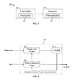
- a CPRL such as for a communication system 20 as shown in Figure 1 that includes a transmitter 22 communicating with a receiver 24.
- the transmitter 22 and receiver 24 are replaced with transceivers capable of both transmission and reception.
- a separate transmitter 22 and receiver 24 are provided.
- the communication system 20 may be used to transmit and receive coded and/or un-coded signals.
- the transmitter 22 includes a modulator 26 for modulating a signal to transmit.
- the receiver 24 includes a demodulator 28 for demodulating the modulated signal received from the transmitter 22.
- the modulation and demodulation performed by the modulator 26 and demodulator 28, respectively, may include using different types of waveform shapes (e.g., raised cosine waveform shape).
- the demodulator 28 is used to recover the original transmitted signal from the transmitter 22.
- the adaptive CPRL 36 includes a Phase-Locked Loop (PLL) 30 that is an electronic control system that generates a signal locked to the phase of an input or reference signal.
- PLL Phase-Locked Loop
- the input signal or reference signal may be a complex waveform having both magnitude and phase information, such as a known repeating sequence of symbols that is modulated. This known repeating sequence of symbols is referred to herein as an amble sequence. It should be appreciated that the amble sequence in the various embodiments is the same for both the input signal and the reference signal.
- the PLL 30 may be any type of PLL device that is configured to recover an original transmitted signal, such as after signal or phase distortion that occurred during transmission of the signal. The PLL 30, thus, operates to lock the receiver into the phase of the input signal.
- phase error vectors 32 that are based on the reference signal and the output of the PLL 30.
- the phase error vectors 32 are input to a MMSE module 34.
- the MMSE module 34 which may be implemented in hardware, software, or a combination thereof, receives as one or more inputs the phase error vectors 32 and has an output connected to the PLL 30.
- the MMSE module 34 may perform an MMSE algorithm to determine an optimal CPRL bandwidth for coded and/or un-coded transmissions.
- the configuration for the MMSE module 34 is different for processing coded and un-coded transmissions.
- Figures 3 and 4 illustrate different embodiments of a CPRL System Model and MMSE algorithm that may be implemented using the MMSE module 34.
- the configuration of Figure 3 is used for coded signals and the configuration of Figure 4 is used for un-coded signals.
- a CPRS 40 shown in Figure 3 is used for waveforms that are transmitted at lower signal-to-noise ratios (SNR), which is generally the case where the waveforms are coded with some form of forward-error correction (FEC).
- a CPRS 80 of Figure 4 is used for waveforms that are transmitted at higher SNR, which is generally the case for waveforms that are un-coded.
- the CPRL bandwidth may be optimized for a plurality of waveforms.
- An SNR threshold value may be used to define whether the SNR is higher or lower than a predetermined or defined value. Other criteria or factors additionally or alternatively may be used, such as whether the signals are coded or un-coded. Accordingly, the SNR threshold value may be variable and/or predetermined or defined. In one embodiment, the SNR threshold value is 5 decibels (dB). In this embodiment, if the SNR is less than 5 dB then the CPRS 40 is selected and if the SNR is greater than or equal to 5 dB then the CPRS 80 is selected. The SNR threshold value may be greater or less than 5 dB (which may be significantly lower or higher) in other embodiments, for example, based on system or communication requirements.
- a selector 100 is provided that selects the output from either the CPRS 40 or the CPRS 80 based on the SNR of the signal.
- the output from the CPRS 40 or the CPRS 80 is then processed by the MMSE module 34.
- the MMSE module 34 may select an MMSE algorithm as described herein based on whether the output is from the CPRS 40 or the CPRS 80.
- the selected MMSE algorithm is used in various embodiments to determine an optimum CPRL bandwidth for the transmission. For example, a desired decision model based on a predetermined SNR may be determined for use in calculating the MMSE.
- Table 1 below includes a list of terms that may be used. Table 1 includes the term, a corresponding symbol or acronym (if any) as used herein and a description of the term for various embodiments. It should be realized that Table 1 is merely used to facilitate a general understanding of the terms and is not limiting.
- Table 1 Term Symbol Description BTs The product of the CPRL loop bandwidth, B , and the symbol time, Ts . BTs i The i th value of BTs from 0.0001 to 1.0; the minimum value is variable (> 0) while the maximum value is 1.0.
- Carrier C A carrier phase recovery loop is used to estimate and Phase Recovery Loop PRL compensate for frequency and phase differences between a received signal's carrier frequency and the receiver's local oscillator phase and frequency for the purpose of non-coherent demodulation.
- CPRL Loop Bandwidth B The loop bandwidth of the CPRL Decision The Decision function selects the constellation coordinate that reflects the minimum distance between the received symbol coordinate and the nearest constellation coordinate.
- Input Signal The Input Signal (or received signal) contains a known, repeating sequence of symbols which is modulated.
- This known repeating sequence of symbols is referred to herein as an amble sequence. This same repeating sequence of symbols is likewise found in the Reference Signal. It is presumed that this repeating sequence of symbols is aligned such that there can be a symbol-by-symbol comparison between each symbol in the Reference Signal and the Input Signal.
- Input Signal is a stream of modulated symbols running at a symbol rate, R s Loop Filter The Loop Filter, filters the output sequence from the Phase Detector.
- Numeric ally Controlled Oscillator N CO The output of the NCO is a phase correction estimate that is used to correct the Input Signal.
- N Number of symbols used to determine the MMSE Output Signal
- Phase function The output of the Phase function is the phase component of the complex input to the Phase function.
- Phase The output of the Phase Detector is a numerical Detector representation of an estimated phase difference between x ( n ) and y ( n ) Reference Signal
- This known repeating sequence of symbols is referred to herein as an amble sequence. This same sequence of symbols is likewise found in the Input Signal.
- the Reference Signal is a stream of symbols running at a symbol rate, Rs .
- Symbol Rate (symbols/sec) Rs Symbol rate is the rate at which the symbol changes per unit time.
- Symbol Time (sec) Ts Ts 1 Rs
- the PLL 30 includes a mixer 42 that receives the input signal and an oscillator signal, which in the illustrated embodiment is generated by a Numerically Controlled Oscillator (NCO) 44.
- the NCO 44 is connected to a loop filter 46, which is connected to a phase detector 48.
- the output of the phase detector 48 connected through the loop filter 46 and the NCO 44 to the mixer 44 form a feedback loop of the PLL 30.
- the output of the mixer 42 is connected to a decision module 50, the output of which is connected to the phase detector 48.
- the phase detector outputs a numerical representation of an estimated phase difference between the signal x(n) input to the decision module 50 and the signal y(n) output from the decision module 50.
- the output of the phase detector 48 is fed through the feedback loop with the loop filter filtering the output sequence from the phase detector 48.
- the filtered output from the loop filter 46 is provided to the NCO 44, which outputs a phase correction estimate used to correct the input signal.
- the PLL 30 responds to a frequency and/or phase of the input signal until the frequency and/or phase of the output signal is matched to the frequency and/or phase of the reference signal.
- the decision module 50 may be configured to select a constellation coordinate that reflects the minimum distance between the received symbol coordinate and the nearest constellation coordinate.
- the PLL 30 may be implemented in different configurations and the components of the PLL 30 are merely for illustration.
- the PLL 30 may be any type of PLL device that performs PLL operations as described herein.
- the x(n) and y(n) signals are output from the PLL 30 and the phase components from the signals extracted by the phase functions 52 and 54, respectively.
- the output of the phase functions 52 and 54 are the phase components of the complex input signal to the phase functions 52 and 54, which includes both magnitude and phase.
- the function may be a hardware component operating to perform the function, a software component to perform the function, or a combination thereof.
- a Phase Error Vector function 60 in the CPRS 40 generates a single output signal (combined signal) and the Phase Error Vector function 62 in the CPRS 80 generates two output signals.
- the Phase Error Vector functions 60 and 62 may be implemented in hardware, software, or a combination thereof, and may be, for example, one or more modules.
- the Phase Error Vector function 60 and/or the Phase Error Vector function 62 may be embodied or implemented as the adaptive CPRL 36 (shown in Figure 1 ).
- a summer 64 is connected to the phase function 52 and to a phase function 66, which outputs the phase component of the reference signal z(n).
- the negative of the phase component of the reference signal is summed with the phase component of the x(n) signal, effectively subtracting the phase component of the reference signal from the phase component of the x(n) signal.
- a summer 66 is connected to the outputs of the phase functions 52 and 54.
- the negative of the phase component of the y(n) signal is added to the phase component of the x(n) signal, effectively subtracting the phase component of the y(n) signal from the phase component of the x(n) signal.
- the outputs from the summers 64 and 68 are also connected to a summer 70.
- the negative of the output of the summer 68 is added to the output of the summer 64 to generate a single signal.
- the output of the summer 70, Phase is connected to mean-squared MS function (MS) 72.
- the output of the MS 72 is a mean-squared error that is input to the MMSE 34.
- the range of BTs may be varied. In one embodiment, the values for the BTs are determined from approximately 0.0001 to 1.0, with defined increments (e.g., 0.05 or 0.1 increments). However, the range may have a higher or lower starting or ending point and the increments may be defined based on the number of samples to be used.
- the outputs of the summers 64 and 68 are connected to an MS 74 and an MS 76, respectively, which performs a similar function to the MS 72 as described above.
- the outputs of the MS 74 and the MS 76 are mean-squared errors that are input to the MMSE 34.
- the MSE Ref and the MSE Rec output from the MS 74 and the MS 76, respectively, may be determined over a plurality of values BTs.
- the range of BTs may be varied. In one embodiment, the values for the BTs are determined from approximately 0.001 to 1.0, with defined increments. However, the range may have a higher or lower starting or ending point and the increments may be defined based on the number of samples to be used.
- the selector 100 selects the signal to communicate to the MMSE 34 based on an SNR threshold, which is 5dB in one embodiment. Accordingly, if the SNR is less than 5dB, the output signal MSE from the MS 72 of the Phase Error Vector function 60 is input to the MMSE 34. If the SNR is greater than or equal to 5dB, the output signals MSE Ref and the MSE Rec from the MS 74 and the MS 76, respectively, of the Phase Error Vector function 62 are input to the MMSE 34.
- an SNR threshold which is 5dB in one embodiment. Accordingly, if the SNR is less than 5dB, the output signal MSE from the MS 72 of the Phase Error Vector function 60 is input to the MMSE 34. If the SNR is greater than or equal to 5dB, the output signals MSE Ref and the MSE Rec from the MS 74 and the MS 76, respectively, of the Phase Error Vector function 62 are input to the MMSE 34.
- the MMSE and optimum loop bandwidth may be determined using different MMSE methods or calculations.
- the MMSE may be determined similar to the MMSE for the output of the Phase Error Vector function 60, such that MMSE is the minimum of the MSE for the determined values of the BTs.
- the output of the MMSE 34 is connected to the loop filter 46 of the CPRS 40 or the CPRS 80.
- estimates may be determined from the noise in the system (e.g., phase noise characteristics at a given moment in time).
- Various embodiments also provide a method 90 as shown in Figure 6 for determining an optimum CPRL bandwidth.
- the method 90 includes receiving a modulated signal at 92.
- a demodulator of a receiver receives a modulated signal.
- a determination is then made at 94 as to whether the transmission is a coded transmission. If the transmission is coded, then a combined MSE is determined at 96. If the transmission is un-coded, then the reference MSE and the received MSE is determined at 98.
- the MSEs may be determined by the CPRLs as described in more detail herein by providing a reference signal and detecting an input signal.
- an MMSE and optimum loop bandwidth over a plurality of BTs i which is the product of the CPRL loop bandwidth and the symbol time, is determined. Based on the MMSE calculations, an optimum CPRL bandwidth value is provided to a PLL, for example, the loop filter 46 of the PLL 30.
- the MMSE is calculated as described herein as a function of SNR. It should be noted that the MMSE Algorithm may be simplified in order to reduce computational resources as described herein.
- the optimization of B is performed for each waveform, where a communication waveform may vary as a function of frequency, symbol rate, data rate, FEC, modulation format (e.g., BPSK, QPSK, etc.), and other factors.
- the optimization of B can be performed for calibration and initialization of a waveform for a given communications channel either one-time, on a determined schedule, or continuously.
- the loop filter 46 may be designed such that B is optimized and set on a one-time basis such as in the case of an analog filter design, or the loop filter 46 may be designed such that B is variable, such as in the case of a filter formed via a digital signal processor.
- various embodiments provide for selection of a CPRL bandwidth based on a measured phase noise.
- a theoretical bandwidth is, thus, not assumed.
- the various embodiments may be implemented in hardware, software or a combination thereof.
- the various embodiments and/or components also may be implemented as part of one or more computers or processors.
- the computer or processor may include a computing device, an input device, a display unit and an interface, for example, for accessing the Internet.
- the computer or processor may include a microprocessor.
- the microprocessor may be connected to a communication bus.
- the computer or processor may also include a memory.
- the memory may include Random Access Memory (RAM) and Read Only Memory (ROM).
- the computer or processor further may include a storage device, which may be a hard disk drive or a removable storage drive such as a solid state drive, optical disk drive, and the like.
- the storage device may also be other similar means for loading computer programs or other instructions into the computer or processor.
- the term "computer” or “module” may include any processor-based or microprocessor-based system including systems using microcontrollers, reduced instruction set computers (RISC), ASICs, logic circuits, and any other circuit or processor capable of executing the functions described herein.
- RISC reduced instruction set computers
- ASIC application specific integrated circuit
- logic circuits logic circuits, and any other circuit or processor capable of executing the functions described herein.
- the above examples are exemplary only, and are thus not intended to limit in any way the definition and/or meaning of the term "computer”.
- the computer or processor executes a set of instructions that are stored in one or more storage elements, in order to process input data.
- the storage elements may also store data or other information as desired or needed.
- the storage element may be in the form of an information source or a physical memory element within a processing machine.
- the set of instructions may include various commands that instruct the computer or processor as a processing machine to perform specific operations such as the methods and processes of the various embodiments.
- the set of instructions may be in the form of a software program.
- the software may be in various forms such as system software or application software and which may be embodied as a tangible and non-transitory computer readable medium. Further, the software may be in the form of a collection of separate programs or modules, a program module within a larger program or a portion of a program module.
- the software also may include modular programming in the form of object-oriented programming.
- the processing of input data by the processing machine may be in response to operator commands, or in response to results of previous processing, or in response to a request made by another processing machine.
- the terms "software” and “firmware” are interchangeable, and include any computer program stored in memory for execution by a computer, including RAM memory, ROM memory, EPROM memory, EEPROM memory, and non-volatile RAM (NVRAM) memory.
- RAM memory random access memory
- ROM memory read-only memory
- EPROM memory erasable programmable read-only memory
- EEPROM memory electrically erasable programmable read-only memory
- NVRAM non-volatile RAM
Landscapes
- Engineering & Computer Science (AREA)
- Computer Networks & Wireless Communication (AREA)
- Signal Processing (AREA)
- Physics & Mathematics (AREA)
- Electromagnetism (AREA)
- Quality & Reliability (AREA)
- Digital Transmission Methods That Use Modulated Carrier Waves (AREA)
Applications Claiming Priority (1)
| Application Number | Priority Date | Filing Date | Title |
|---|---|---|---|
| US13/599,806 US9042490B2 (en) | 2012-08-30 | 2012-08-30 | Systems and methods for carrier phase recovery |
Publications (2)
| Publication Number | Publication Date |
|---|---|
| EP2704385A1 true EP2704385A1 (de) | 2014-03-05 |
| EP2704385B1 EP2704385B1 (de) | 2021-01-13 |
Family
ID=49000825
Family Applications (1)
| Application Number | Title | Priority Date | Filing Date |
|---|---|---|---|
| EP13180701.8A Active EP2704385B1 (de) | 2012-08-30 | 2013-08-16 | Systeme und Verfahren zur Auswahl der Schleifenfilterbandbreite zur Rückgewinnung der Trägerphase |
Country Status (2)
| Country | Link |
|---|---|
| US (1) | US9042490B2 (de) |
| EP (1) | EP2704385B1 (de) |
Families Citing this family (3)
| Publication number | Priority date | Publication date | Assignee | Title |
|---|---|---|---|---|
| TWI631826B (zh) * | 2017-03-22 | 2018-08-01 | 晨星半導體股份有限公司 | 頻寬調整方法與相關的頻寬調整單元及相位回復模組 |
| TW201943212A (zh) * | 2018-03-31 | 2019-11-01 | 晨星半導體股份有限公司 | 信號接收裝置及其信號處理方法 |
| CN110460551A (zh) * | 2019-02-24 | 2019-11-15 | 苏州工业园区新国大研究院 | 一种基于最小均方误差的信道载波相位恢复方法 |
Citations (6)
| Publication number | Priority date | Publication date | Assignee | Title |
|---|---|---|---|---|
| EP1201066A1 (de) * | 2000-04-17 | 2002-05-02 | Atmel Corporation | Schätzung des phasen- und überlagerten rauschens in einer qam-trägerrückgewinnungsschaltung |
| EP1241846A2 (de) * | 2001-03-15 | 2002-09-18 | Texas Instruments Incorporated | Initialisierung einer Phasenregelschleife mittels Kurvenanpassung |
| US20050141646A1 (en) * | 2003-12-01 | 2005-06-30 | Lg Electronics Inc. | Carrier recovery apparatus and digital broadcast receiver using the same |
| US20050157820A1 (en) * | 2004-01-15 | 2005-07-21 | Supat Wongwirawat | Digital receiver having adaptive carrier recovery circuit |
| US20120106611A1 (en) * | 2010-10-29 | 2012-05-03 | Texas Instruments Incorporated | Phase locking loop |
| US20120106983A1 (en) * | 2010-11-03 | 2012-05-03 | Nec Laboratories America, Inc. | Optimized normalized least mean square phase estimation |
Family Cites Families (8)
| Publication number | Priority date | Publication date | Assignee | Title |
|---|---|---|---|---|
| FR2505111B1 (fr) | 1981-04-29 | 1986-04-18 | Labo Electronique Physique | Dispositif de recuperation de porteuse pour une modulation d'amplitude et de phase a seize etats et systeme de reception de donnees numeriques comprenant un tel dispositif |
| US6549594B1 (en) | 1999-05-28 | 2003-04-15 | Nortel Networks | Timing phase recovery method and apparatus |
| US6560303B1 (en) | 2000-10-26 | 2003-05-06 | Comsat Corporation | Joint frame, carrier and clock synchronization scheme |
| US7260330B2 (en) | 2002-11-04 | 2007-08-21 | The Boeing Company | Optical communication system using correlation receiver |
| US7526019B1 (en) | 2003-03-27 | 2009-04-28 | Broadlogic Network Technologies Inc. | Method and system for providing multi-channel multimode QAM equalization and carrier recovery |
| US7649952B1 (en) | 2004-07-01 | 2010-01-19 | Regents Of The University Of Minnesota | Low complexity soft demapping |
| KR100660839B1 (ko) | 2004-10-07 | 2006-12-26 | 삼성전자주식회사 | Atsc 수신기에서의 결합된 심볼 타이밍 및 캐리어위상 복원 회로 |
| US7782255B2 (en) | 2007-10-23 | 2010-08-24 | The Boeing Company | System and methods for radar and communications applications |
-
2012
- 2012-08-30 US US13/599,806 patent/US9042490B2/en active Active
-
2013
- 2013-08-16 EP EP13180701.8A patent/EP2704385B1/de active Active
Patent Citations (6)
| Publication number | Priority date | Publication date | Assignee | Title |
|---|---|---|---|---|
| EP1201066A1 (de) * | 2000-04-17 | 2002-05-02 | Atmel Corporation | Schätzung des phasen- und überlagerten rauschens in einer qam-trägerrückgewinnungsschaltung |
| EP1241846A2 (de) * | 2001-03-15 | 2002-09-18 | Texas Instruments Incorporated | Initialisierung einer Phasenregelschleife mittels Kurvenanpassung |
| US20050141646A1 (en) * | 2003-12-01 | 2005-06-30 | Lg Electronics Inc. | Carrier recovery apparatus and digital broadcast receiver using the same |
| US20050157820A1 (en) * | 2004-01-15 | 2005-07-21 | Supat Wongwirawat | Digital receiver having adaptive carrier recovery circuit |
| US20120106611A1 (en) * | 2010-10-29 | 2012-05-03 | Texas Instruments Incorporated | Phase locking loop |
| US20120106983A1 (en) * | 2010-11-03 | 2012-05-03 | Nec Laboratories America, Inc. | Optimized normalized least mean square phase estimation |
Non-Patent Citations (1)
| Title |
|---|
| KIM B ED - INSTITUTE OF ELECTRICAL AND ELECTRONICS ENGINEERS: "Optical MMSE gear-shifting algorithm for the fast synchronization of DPLL", PROCEEDINGS OF THE INTERNATIONAL SYMPOSIUM ON CIRCUITS AND SYSTEMS. (ISCS). CHICAGO, MAY 3 - 6, 1993; [PROCEEDINGS OF THE INTERNATIONAL SYMPOSIUM ON CIRCUITS AND SYSTEMS. (ISCS)], NEW YORK, IEEE, US, vol. -, 3 May 1993 (1993-05-03), pages 172 - 175, XP010115130, ISBN: 978-0-7803-1281-4, DOI: 10.1109/ISCAS.1993.393685 * |
Also Published As
| Publication number | Publication date |
|---|---|
| EP2704385B1 (de) | 2021-01-13 |
| US9042490B2 (en) | 2015-05-26 |
| US20140064347A1 (en) | 2014-03-06 |
Similar Documents
| Publication | Publication Date | Title |
|---|---|---|
| US9130627B2 (en) | Multi-mode receiver for highly-spectrally-efficient communications | |
| US8675778B2 (en) | Carrier recovery circuit and demodulation circuit under quasi-coherent detection method | |
| EP3706380B1 (de) | Detektor von fehlern der frequenzumtastung (fsk) und verfahren dafür | |
| US8798211B2 (en) | Channel-sensitive power control | |
| US8265192B2 (en) | Multilevel QAM demodulator, multilevel QAM demodulation method, and wireless communication system | |
| EP2704385B1 (de) | Systeme und Verfahren zur Auswahl der Schleifenfilterbandbreite zur Rückgewinnung der Trägerphase | |
| US8718206B2 (en) | Frequency correction circuit, frequency correction method and wireless communication equipment using them | |
| CN101378288B (zh) | 偏差推测装置 | |
| JP5190113B2 (ja) | ワイヤレス通信システムにおける送信処理 | |
| US9231805B2 (en) | Device for carrier phase recovery | |
| JP4985535B2 (ja) | 復調回路 | |
| EP1420558B1 (de) | Empfangseinrichtung, Demodulator und Kommunikationsverfahren | |
| CN104242928B (zh) | 锁频环中一种基于叉积算法的频率锁定检测器处理方法 | |
| Dan et al. | On the blind SNR estimation for IF signals | |
| US20060133291A1 (en) | Method and system for determining a signal quality metric in event of a CRC false positive | |
| JP7696680B2 (ja) | 復調回路 | |
| US8290090B2 (en) | Blind amplitude estimation for received symbols | |
| JP2005236666A (ja) | Ofdm復調装置 | |
| JP4813966B2 (ja) | Afc回路 | |
| JP6643770B2 (ja) | 周波数オフセット推定装置および無線通信装置 | |
| JP3355147B2 (ja) | 自動周波数制御方式 | |
| CN120415971A (zh) | 一种针对apsk内外圈相位不一致的修正方法和装置 | |
| JPH10200591A (ja) | 自動周波数制御回路 | |
| JP2000236365A (ja) | 歪み推定装置とそれを用いた復調装置 |
Legal Events
| Date | Code | Title | Description |
|---|---|---|---|
| 17P | Request for examination filed |
Effective date: 20130816 |
|
| AK | Designated contracting states |
Kind code of ref document: A1 Designated state(s): AL AT BE BG CH CY CZ DE DK EE ES FI FR GB GR HR HU IE IS IT LI LT LU LV MC MK MT NL NO PL PT RO RS SE SI SK SM TR |
|
| AX | Request for extension of the european patent |
Extension state: BA ME |
|
| PUAI | Public reference made under article 153(3) epc to a published international application that has entered the european phase |
Free format text: ORIGINAL CODE: 0009012 |
|
| STAA | Information on the status of an ep patent application or granted ep patent |
Free format text: STATUS: EXAMINATION IS IN PROGRESS |
|
| 17Q | First examination report despatched |
Effective date: 20170220 |
|
| GRAP | Despatch of communication of intention to grant a patent |
Free format text: ORIGINAL CODE: EPIDOSNIGR1 |
|
| STAA | Information on the status of an ep patent application or granted ep patent |
Free format text: STATUS: GRANT OF PATENT IS INTENDED |
|
| INTG | Intention to grant announced |
Effective date: 20200716 |
|
| GRAS | Grant fee paid |
Free format text: ORIGINAL CODE: EPIDOSNIGR3 |
|
| GRAJ | Information related to disapproval of communication of intention to grant by the applicant or resumption of examination proceedings by the epo deleted |
Free format text: ORIGINAL CODE: EPIDOSDIGR1 |
|
| GRAL | Information related to payment of fee for publishing/printing deleted |
Free format text: ORIGINAL CODE: EPIDOSDIGR3 |
|
| STAA | Information on the status of an ep patent application or granted ep patent |
Free format text: STATUS: EXAMINATION IS IN PROGRESS |
|
| GRAP | Despatch of communication of intention to grant a patent |
Free format text: ORIGINAL CODE: EPIDOSNIGR1 |
|
| STAA | Information on the status of an ep patent application or granted ep patent |
Free format text: STATUS: GRANT OF PATENT IS INTENDED |
|
| GRAA | (expected) grant |
Free format text: ORIGINAL CODE: 0009210 |
|
| STAA | Information on the status of an ep patent application or granted ep patent |
Free format text: STATUS: THE PATENT HAS BEEN GRANTED |
|
| INTC | Intention to grant announced (deleted) | ||
| INTG | Intention to grant announced |
Effective date: 20201127 |
|
| AK | Designated contracting states |
Kind code of ref document: B1 Designated state(s): AL AT BE BG CH CY CZ DE DK EE ES FI FR GB GR HR HU IE IS IT LI LT LU LV MC MK MT NL NO PL PT RO RS SE SI SK SM TR |
|
| REG | Reference to a national code |
Ref country code: GB Ref legal event code: FG4D |
|
| REG | Reference to a national code |
Ref country code: CH Ref legal event code: EP |
|
| REG | Reference to a national code |
Ref country code: IE Ref legal event code: FG4D |
|
| REG | Reference to a national code |
Ref country code: DE Ref legal event code: R096 Ref document number: 602013075265 Country of ref document: DE |
|
| REG | Reference to a national code |
Ref country code: AT Ref legal event code: REF Ref document number: 1355372 Country of ref document: AT Kind code of ref document: T Effective date: 20210215 |
|
| REG | Reference to a national code |
Ref country code: AT Ref legal event code: MK05 Ref document number: 1355372 Country of ref document: AT Kind code of ref document: T Effective date: 20210113 |
|
| REG | Reference to a national code |
Ref country code: NL Ref legal event code: MP Effective date: 20210113 |
|
| REG | Reference to a national code |
Ref country code: LT Ref legal event code: MG9D |
|
| PG25 | Lapsed in a contracting state [announced via postgrant information from national office to epo] |
Ref country code: GR Free format text: LAPSE BECAUSE OF FAILURE TO SUBMIT A TRANSLATION OF THE DESCRIPTION OR TO PAY THE FEE WITHIN THE PRESCRIBED TIME-LIMIT Effective date: 20210414 Ref country code: FI Free format text: LAPSE BECAUSE OF FAILURE TO SUBMIT A TRANSLATION OF THE DESCRIPTION OR TO PAY THE FEE WITHIN THE PRESCRIBED TIME-LIMIT Effective date: 20210113 Ref country code: HR Free format text: LAPSE BECAUSE OF FAILURE TO SUBMIT A TRANSLATION OF THE DESCRIPTION OR TO PAY THE FEE WITHIN THE PRESCRIBED TIME-LIMIT Effective date: 20210113 Ref country code: PT Free format text: LAPSE BECAUSE OF FAILURE TO SUBMIT A TRANSLATION OF THE DESCRIPTION OR TO PAY THE FEE WITHIN THE PRESCRIBED TIME-LIMIT Effective date: 20210513 Ref country code: LT Free format text: LAPSE BECAUSE OF FAILURE TO SUBMIT A TRANSLATION OF THE DESCRIPTION OR TO PAY THE FEE WITHIN THE PRESCRIBED TIME-LIMIT Effective date: 20210113 Ref country code: BG Free format text: LAPSE BECAUSE OF FAILURE TO SUBMIT A TRANSLATION OF THE DESCRIPTION OR TO PAY THE FEE WITHIN THE PRESCRIBED TIME-LIMIT Effective date: 20210413 Ref country code: NL Free format text: LAPSE BECAUSE OF FAILURE TO SUBMIT A TRANSLATION OF THE DESCRIPTION OR TO PAY THE FEE WITHIN THE PRESCRIBED TIME-LIMIT Effective date: 20210113 Ref country code: NO Free format text: LAPSE BECAUSE OF FAILURE TO SUBMIT A TRANSLATION OF THE DESCRIPTION OR TO PAY THE FEE WITHIN THE PRESCRIBED TIME-LIMIT Effective date: 20210413 |
|
| PG25 | Lapsed in a contracting state [announced via postgrant information from national office to epo] |
Ref country code: SE Free format text: LAPSE BECAUSE OF FAILURE TO SUBMIT A TRANSLATION OF THE DESCRIPTION OR TO PAY THE FEE WITHIN THE PRESCRIBED TIME-LIMIT Effective date: 20210113 Ref country code: RS Free format text: LAPSE BECAUSE OF FAILURE TO SUBMIT A TRANSLATION OF THE DESCRIPTION OR TO PAY THE FEE WITHIN THE PRESCRIBED TIME-LIMIT Effective date: 20210113 Ref country code: LV Free format text: LAPSE BECAUSE OF FAILURE TO SUBMIT A TRANSLATION OF THE DESCRIPTION OR TO PAY THE FEE WITHIN THE PRESCRIBED TIME-LIMIT Effective date: 20210113 Ref country code: PL Free format text: LAPSE BECAUSE OF FAILURE TO SUBMIT A TRANSLATION OF THE DESCRIPTION OR TO PAY THE FEE WITHIN THE PRESCRIBED TIME-LIMIT Effective date: 20210113 Ref country code: AT Free format text: LAPSE BECAUSE OF FAILURE TO SUBMIT A TRANSLATION OF THE DESCRIPTION OR TO PAY THE FEE WITHIN THE PRESCRIBED TIME-LIMIT Effective date: 20210113 |
|
| PG25 | Lapsed in a contracting state [announced via postgrant information from national office to epo] |
Ref country code: IS Free format text: LAPSE BECAUSE OF FAILURE TO SUBMIT A TRANSLATION OF THE DESCRIPTION OR TO PAY THE FEE WITHIN THE PRESCRIBED TIME-LIMIT Effective date: 20210513 |
|
| REG | Reference to a national code |
Ref country code: DE Ref legal event code: R097 Ref document number: 602013075265 Country of ref document: DE |
|
| PG25 | Lapsed in a contracting state [announced via postgrant information from national office to epo] |
Ref country code: SM Free format text: LAPSE BECAUSE OF FAILURE TO SUBMIT A TRANSLATION OF THE DESCRIPTION OR TO PAY THE FEE WITHIN THE PRESCRIBED TIME-LIMIT Effective date: 20210113 Ref country code: CZ Free format text: LAPSE BECAUSE OF FAILURE TO SUBMIT A TRANSLATION OF THE DESCRIPTION OR TO PAY THE FEE WITHIN THE PRESCRIBED TIME-LIMIT Effective date: 20210113 Ref country code: EE Free format text: LAPSE BECAUSE OF FAILURE TO SUBMIT A TRANSLATION OF THE DESCRIPTION OR TO PAY THE FEE WITHIN THE PRESCRIBED TIME-LIMIT Effective date: 20210113 |
|
| PLBE | No opposition filed within time limit |
Free format text: ORIGINAL CODE: 0009261 |
|
| STAA | Information on the status of an ep patent application or granted ep patent |
Free format text: STATUS: NO OPPOSITION FILED WITHIN TIME LIMIT |
|
| PG25 | Lapsed in a contracting state [announced via postgrant information from national office to epo] |
Ref country code: RO Free format text: LAPSE BECAUSE OF FAILURE TO SUBMIT A TRANSLATION OF THE DESCRIPTION OR TO PAY THE FEE WITHIN THE PRESCRIBED TIME-LIMIT Effective date: 20210113 Ref country code: ES Free format text: LAPSE BECAUSE OF FAILURE TO SUBMIT A TRANSLATION OF THE DESCRIPTION OR TO PAY THE FEE WITHIN THE PRESCRIBED TIME-LIMIT Effective date: 20210113 Ref country code: DK Free format text: LAPSE BECAUSE OF FAILURE TO SUBMIT A TRANSLATION OF THE DESCRIPTION OR TO PAY THE FEE WITHIN THE PRESCRIBED TIME-LIMIT Effective date: 20210113 Ref country code: SK Free format text: LAPSE BECAUSE OF FAILURE TO SUBMIT A TRANSLATION OF THE DESCRIPTION OR TO PAY THE FEE WITHIN THE PRESCRIBED TIME-LIMIT Effective date: 20210113 |
|
| 26N | No opposition filed |
Effective date: 20211014 |
|
| PG25 | Lapsed in a contracting state [announced via postgrant information from national office to epo] |
Ref country code: AL Free format text: LAPSE BECAUSE OF FAILURE TO SUBMIT A TRANSLATION OF THE DESCRIPTION OR TO PAY THE FEE WITHIN THE PRESCRIBED TIME-LIMIT Effective date: 20210113 |
|
| PG25 | Lapsed in a contracting state [announced via postgrant information from national office to epo] |
Ref country code: SI Free format text: LAPSE BECAUSE OF FAILURE TO SUBMIT A TRANSLATION OF THE DESCRIPTION OR TO PAY THE FEE WITHIN THE PRESCRIBED TIME-LIMIT Effective date: 20210113 |
|
| REG | Reference to a national code |
Ref country code: CH Ref legal event code: PL |
|
| PG25 | Lapsed in a contracting state [announced via postgrant information from national office to epo] |
Ref country code: MC Free format text: LAPSE BECAUSE OF FAILURE TO SUBMIT A TRANSLATION OF THE DESCRIPTION OR TO PAY THE FEE WITHIN THE PRESCRIBED TIME-LIMIT Effective date: 20210113 |
|
| REG | Reference to a national code |
Ref country code: BE Ref legal event code: MM Effective date: 20210831 |
|
| PG25 | Lapsed in a contracting state [announced via postgrant information from national office to epo] |
Ref country code: LI Free format text: LAPSE BECAUSE OF NON-PAYMENT OF DUE FEES Effective date: 20210831 Ref country code: IT Free format text: LAPSE BECAUSE OF FAILURE TO SUBMIT A TRANSLATION OF THE DESCRIPTION OR TO PAY THE FEE WITHIN THE PRESCRIBED TIME-LIMIT Effective date: 20210113 Ref country code: CH Free format text: LAPSE BECAUSE OF NON-PAYMENT OF DUE FEES Effective date: 20210831 |
|
| PG25 | Lapsed in a contracting state [announced via postgrant information from national office to epo] |
Ref country code: IS Free format text: LAPSE BECAUSE OF FAILURE TO SUBMIT A TRANSLATION OF THE DESCRIPTION OR TO PAY THE FEE WITHIN THE PRESCRIBED TIME-LIMIT Effective date: 20210513 Ref country code: LU Free format text: LAPSE BECAUSE OF NON-PAYMENT OF DUE FEES Effective date: 20210816 |
|
| PG25 | Lapsed in a contracting state [announced via postgrant information from national office to epo] |
Ref country code: IE Free format text: LAPSE BECAUSE OF NON-PAYMENT OF DUE FEES Effective date: 20210816 Ref country code: BE Free format text: LAPSE BECAUSE OF NON-PAYMENT OF DUE FEES Effective date: 20210831 |
|
| PG25 | Lapsed in a contracting state [announced via postgrant information from national office to epo] |
Ref country code: HU Free format text: LAPSE BECAUSE OF FAILURE TO SUBMIT A TRANSLATION OF THE DESCRIPTION OR TO PAY THE FEE WITHIN THE PRESCRIBED TIME-LIMIT; INVALID AB INITIO Effective date: 20130816 |
|
| P01 | Opt-out of the competence of the unified patent court (upc) registered |
Effective date: 20230516 |
|
| PG25 | Lapsed in a contracting state [announced via postgrant information from national office to epo] |
Ref country code: CY Free format text: LAPSE BECAUSE OF FAILURE TO SUBMIT A TRANSLATION OF THE DESCRIPTION OR TO PAY THE FEE WITHIN THE PRESCRIBED TIME-LIMIT Effective date: 20210113 |
|
| PG25 | Lapsed in a contracting state [announced via postgrant information from national office to epo] |
Ref country code: MK Free format text: LAPSE BECAUSE OF FAILURE TO SUBMIT A TRANSLATION OF THE DESCRIPTION OR TO PAY THE FEE WITHIN THE PRESCRIBED TIME-LIMIT Effective date: 20210113 |
|
| PG25 | Lapsed in a contracting state [announced via postgrant information from national office to epo] |
Ref country code: TR Free format text: LAPSE BECAUSE OF FAILURE TO SUBMIT A TRANSLATION OF THE DESCRIPTION OR TO PAY THE FEE WITHIN THE PRESCRIBED TIME-LIMIT Effective date: 20210113 |
|
| PG25 | Lapsed in a contracting state [announced via postgrant information from national office to epo] |
Ref country code: MT Free format text: LAPSE BECAUSE OF FAILURE TO SUBMIT A TRANSLATION OF THE DESCRIPTION OR TO PAY THE FEE WITHIN THE PRESCRIBED TIME-LIMIT Effective date: 20210113 |
|
| PGFP | Annual fee paid to national office [announced via postgrant information from national office to epo] |
Ref country code: DE Payment date: 20250827 Year of fee payment: 13 |
|
| PGFP | Annual fee paid to national office [announced via postgrant information from national office to epo] |
Ref country code: GB Payment date: 20250827 Year of fee payment: 13 |
|
| PGFP | Annual fee paid to national office [announced via postgrant information from national office to epo] |
Ref country code: FR Payment date: 20250825 Year of fee payment: 13 |