EP2706426A2 - Circuit de référence de tension sans résistance à basse puissance - Google Patents
Circuit de référence de tension sans résistance à basse puissance Download PDFInfo
- Publication number
- EP2706426A2 EP2706426A2 EP13182995.4A EP13182995A EP2706426A2 EP 2706426 A2 EP2706426 A2 EP 2706426A2 EP 13182995 A EP13182995 A EP 13182995A EP 2706426 A2 EP2706426 A2 EP 2706426A2
- Authority
- EP
- European Patent Office
- Prior art keywords
- voltage
- circuit
- pseudo resistor
- pseudo
- transistor
- Prior art date
- Legal status (The legal status is an assumption and is not a legal conclusion. Google has not performed a legal analysis and makes no representation as to the accuracy of the status listed.)
- Withdrawn
Links
Images


Classifications
-
- G—PHYSICS
- G05—CONTROLLING; REGULATING
- G05F—SYSTEMS FOR REGULATING ELECTRIC OR MAGNETIC VARIABLES
- G05F3/00—Non-retroactive systems for regulating electric variables by using an uncontrolled element, or an uncontrolled combination of elements, such element or such combination having self-regulating properties
- G05F3/02—Regulating voltage or current
- G05F3/08—Regulating voltage or current wherein the variable is DC
- G05F3/10—Regulating voltage or current wherein the variable is DC using uncontrolled devices with non-linear characteristics
- G05F3/16—Regulating voltage or current wherein the variable is DC using uncontrolled devices with non-linear characteristics being semiconductor devices
- G05F3/20—Regulating voltage or current wherein the variable is DC using uncontrolled devices with non-linear characteristics being semiconductor devices using diode- transistor combinations
- G05F3/24—Regulating voltage or current wherein the variable is DC using uncontrolled devices with non-linear characteristics being semiconductor devices using diode- transistor combinations wherein the transistors are of the field-effect type only
- G05F3/242—Regulating voltage or current wherein the variable is DC using uncontrolled devices with non-linear characteristics being semiconductor devices using diode- transistor combinations wherein the transistors are of the field-effect type only with compensation for device parameters, e.g. channel width modulation, threshold voltage, processing, or external variations, e.g. temperature, loading, supply voltage
-
- G—PHYSICS
- G05—CONTROLLING; REGULATING
- G05F—SYSTEMS FOR REGULATING ELECTRIC OR MAGNETIC VARIABLES
- G05F3/00—Non-retroactive systems for regulating electric variables by using an uncontrolled element, or an uncontrolled combination of elements, such element or such combination having self-regulating properties
- G05F3/02—Regulating voltage or current
- G05F3/08—Regulating voltage or current wherein the variable is DC
- G05F3/10—Regulating voltage or current wherein the variable is DC using uncontrolled devices with non-linear characteristics
- G05F3/16—Regulating voltage or current wherein the variable is DC using uncontrolled devices with non-linear characteristics being semiconductor devices
- G05F3/20—Regulating voltage or current wherein the variable is DC using uncontrolled devices with non-linear characteristics being semiconductor devices using diode- transistor combinations
- G05F3/30—Regulators using the difference between the base-emitter voltages of two bipolar transistors operating at different current densities
Definitions
- CMOS complementary metal-oxide-semiconductor
- Voltage reference circuits are important building blocks of microchips because the voltage reference circuits provide a constant voltage regardless of process variation, temperature changes, power supply variations, and time.
- the reference voltage produced by a voltage reference circuit can be compared to output voltages of other components in the microchips to assure accuracy or to perform measurements.
- voltage regulators use a reference voltage to compare a given output voltage to the reference voltage in order to create a temperature independent, constant output supply voltage.
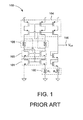
- a conventional reference voltage circuit 100 is shown in Fig. 1 .
- the conventional voltage reference circuit 100 includes a set of resistors 102 that receive current from a current mirror circuit 104. The absolute value of the current is determined by a transistor pair 101 and resistor R 1 .
- the conventional voltage reference circuit 100 is able to output a reference voltage 106, also referred to as V out , based on the current value and a ratio of the resistor values, as well as other characteristics of the circuit.
- Reference voltage circuits are able to take advantage of CMOS technologies to generate a temperature independent, constant output voltage. Aspects of the invention are defined in the claims.
- the circuit is a low power, resistor-less voltage reference circuit.
- the voltage reference circuit includes a proportional-to-absolute-temperature (PTAT) voltage generator configured to produce a PTAT voltage across a first pseudo resistor.
- the first pseudo resistor includes a transistor.
- the PTAT voltage across the first pseudo resistor produces a current based on a resistance of the first pseudo resistor.
- the voltage reference circuit also includes a current mirror circuit configured to mirror the current.
- the voltage reference circuit also includes a second pseudo resistor comprising a transistor. The second pseudo resistor is used to convert the mirrored current to the PTAT voltage.
- the first pseudo resistor and the second pseudo resistor have equal transistor types.
- the voltage reference circuit also includes a complimentary-to-absolute-temperature (CTAT) voltage generator configured to produce a CTAT voltage.
- CTAT complimentary-to-absolute-temperature
- the CTAT voltage is summed with the converted PTAT voltage to produce the reference voltage.
- the reference voltage is temperature independent.
- Other embodiments of a circuit are also described.
- the system includes an electronic circuit configured to generate an output voltage.
- the system also includes a voltage reference circuit.
- the voltage reference circuit includes a proportional-to-absolute-temperature (PTAT) voltage generator configured to produce a PTAT voltage across a first pseudo resistor.
- the first pseudo resistor includes a transistor.
- the PTAT voltage across the first pseudo resistor produces a current based on a resistance of the first pseudo resistor.
- the voltage reference circuit also includes a current mirror circuit configured to mirror the current.
- the voltage reference circuit also includes a second pseudo resistor comprising a transistor. The second pseudo resistor is used to convert the mirrored current to the PTAT voltage.
- the first pseudo resistor and the second pseudo resistor have equal transistor types.
- the voltage reference circuit also includes a complimentary-to-absolute-temperature (CTAT) voltage generator configured to produce a CTAT voltage.
- CTAT complimentary-to-absolute-temperature
- the CTAT voltage is summed with the converted PTAT voltage to produce the reference voltage.
- the reference voltage is temperature independent.
- the system also includes a comparator configured to compare the output voltage of the electronic circuit to the reference voltage. Other embodiments of a system are also described.
- the method is a method for generating a reference voltage.
- the method includes generating a proportional-to-absolute temperature (PTAT) voltage across a first pseudo resistor.
- the first pseudo resistor includes a transistor.
- the method also includes converting the PTAT voltage to a current based on a resistance of the first pseudo resistor.
- the method also includes mirroring the current using a current mirror circuit and converting the mirrored current to the PTAT voltage using a second pseudo resistor.
- the second pseudo resistor includes a transistor.
- the first pseudo resistor and the second pseudo resistor include equal transistor types.
- the method also includes generating a complimentary-to-absolute temperature (CTAT) voltage, and summing the converted PTAT voltage and the CTAT voltage to produce the reference voltage.
- CTAT complimentary-to-absolute temperature
- Other embodiments of a method are also described.
- the system uses a voltage reference circuit to produce the reference voltage using pseudo resistors in different legs of a current mirror circuit.
- the pseudo resistors include transistors that have an associated resistance.
- the system uses transistors in the pseudo resistors of the same transistor type and biases the gate and source voltages to the same potential to produce the desired reference voltage.
- the reference voltage 106 is based in large part on the values of the resistors 102 and the ratio of the resistors values.
- the reference voltage 106 includes a pair 101 of transistors biased with the same gate voltage but different source voltages.
- the pair 101 of transistors creates an accurate PTAT voltage when biased in sub-threshold mode.
- the pair 101 of transistors and the resistor R 1 make up the PTAT voltage generator in the conventional voltage reference circuit 100.
- Additional resistors 108 are sometimes used to implement a self-biased cascode for the current mirror circuit 104 and for the cascode transistors 103.
- the cascode transistors 103 may also be operating in sub-threshold mode.
- the resistor sizes are large. Large resistor sizes can be expensive in plain CMOS technologies. High resistivity material may not be available in plain CMOS technologies, and can be an expensive process option to add.
- resistor matching in standard CMOS technologies tends to be worse than transistor matching. Because very low power reference circuits built with resistors also result in circuits that are physically larger than CMOS components, the resistors may be more susceptible to processing gradients, which further reduces matching accuracy. Additionally, producing very small currents may require the use of minimum width resistors to maximize the length/width ration of the resistors to maximize the resistance. Such parameters usually result in degraded matching performance, and thus, degraded accuracy of the reference voltage.
- CMOS transistors as pseudo resistors, rather than standard resistors, to generate a reference voltage 106 may result in lower power consumption, reduced circuit size, improved accuracy, and less expensive manufacturing, while still providing a temperature independent, constant reference voltage for low power circuits.
- Fig. 2 depicts a block diagram of one embodiment of a system 200 for comparing an output voltage 208 to a reference voltage 106.
- the system includes a voltage reference circuit 202 according to the principles described herein, an electronic circuit 204 other than the voltage reference circuit 202, and a comparator 206.
- the system 200 may be any system that includes at least one electronic circuit 204 whose output voltage 208 is compared to the reference voltage 106 produced by a voltage reference circuit 202 at the comparator 206.
- the reference voltage 106 may be used for other purposes.
- the system 200 may be a subsystem in a larger system or part of a larger component.
- the system 200 may be used to reduce the power consumption of a low power circuit.
- the system 200 helps reduce the standby current of low-power, mixed-signal microcontrollers. During a standby mode, certain tasks may have to be accomplished with minimum impact on power consumption.
- the system 200 may be used for tasks including, but not limited to, voltage regulation, power monitoring, pin-status monitoring, real-time clock applications, and data logging.
- the voltage reference circuit 202 and a simple driver stage may be combined to create a low power voltage regulator that is able to maintain some status and control registers alive/operating during power down of the larger system.
- the voltage reference circuit 202 may be used in a power management unit (PMU) in regulators responsible for state retention during power down, power for control registers, real time clock power, and other important tasks.
- PMU power management unit
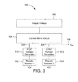
- Fig. 3 depicts a block diagram of one embodiment of the voltage reference circuit 202 of Fig. 2 . While the system 200 is described in conjunction with the voltage reference circuit 202 of Fig. 2 , the system 200 may be used in conjunction with any voltage reference circuit 202, according to the principles described herein. Conversely, the voltage reference circuit 202 of Fig. 2 may be used in conjunction with any electronic system and with any other electronic devices or components.
- the voltage reference circuit 202 includes a supply voltage 300, a current mirror circuit 104, at least two pseudo resistors 302, 304 located on separate legs 306, 308 of the current mirror circuit 104, a proportional-to-absolute-temperature (PTAT) voltage generator 310 on the first leg 306 above the first pseudo resistor 302, and a complimentary-to-absolute-temperature (CTAT) voltage generator 312 on the second leg 308 above the second pseudo resistor 304.
- PTAT proportional-to-absolute-temperature
- CTAT complimentary-to-absolute-temperature
- the current mirror circuit 104 is connected to the supply voltage 300.
- the supply voltage 300 may be any type of supply voltage 300, including a positive supply voltage 300 or a negative supply voltage 300.
- the implementation is complementary to the voltage reference circuit 202 depicted in Fig. 4 , such that the PMOS and NMOS transistors are swapped out.
- the reference voltage 106 generated by configuring the voltage reference circuit 202 with a negative supply voltage 300 may be ground-based.
- the PTAT voltage generator 310 on the first leg 306 is configured to produce a specific voltage across the first pseudo resistor 302, which may be connected to ground.
- the first pseudo resistor 302 and the second pseudo resistor 304 refer to the same voltage potential, such that the first pseudo resistor 302 and the second pseudo resistor 304 are both connected to ground.
- the first pseudo resistor 302 then converts the PTAT voltage to a current.
- the current mirror circuit 104 copies the current across multiple legs, such that each leg has the same current or a scaled version of the copied current.
- the current in the first leg 306 of the current mirror circuit 104 is based on the PTAT voltage and the resistance value of the first pseudo resistor 302.
- the first pseudo resistor 302, as described herein, includes at least one transistor.
- the transistor may have a nonlinear resistivity that influences the current.
- the second pseudo resistor 304 on the second leg 308 of the current mirror circuit 104 also includes a transistor of the same type as the transistor of the first pseudo resistor 302. Because the transistors have the same type, and because their gate-source voltages are identical, undesired effects due to the nonlinear resistivity of the transistors cancels. Additionally, the second leg 308 includes the CTAT voltage generator 312.
- the transistors in the CTAT voltage generator 312 may be operating in sub-threshold mode.
- the reference voltage 106 output by the voltage reference circuit 202 which is produced by summing the PTAT voltage, which has been converted back from the mirrored current according to a predetermined ratio, across the second pseudo resistor 304 with the CTAT voltage, is temperature independent.
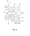
- Fig. 4 depicts a schematic diagram of one embodiment of the voltage reference circuit 202 of Fig. 2 . While the system 200 is described in conjunction with the voltage reference circuit 202 of Fig. 4 , the system 200 may be used in conjunction with any voltage reference circuit 202, according to the principles described herein. Conversely, the voltage reference circuit 202 of Fig. 4 may be used in conjunction with any electronic system and with any other electronic devices or components.
- the voltage reference circuit 202 may be a voltage reference circuit that uses various types of CMOS technologies, including n-type transistors (NMOS) and p-type transistors (PMOS).
- the voltage reference circuit 202 includes a cascode current mirror circuit 104.
- the cascode current mirror circuit 104 may include several cascode transistors pairs.
- the cascode current mirror circuit 104 may reduce dependencies on the voltage produced by the supply voltage 300 and the temperature of the components.
- Other types of current mirror circuits 104 may be used in the voltage reference circuit 202 to copy a current to one or more legs.
- the current in all legs connected to the current mirror circuit 104 are equal with a current mirror ratio of one. Other embodiments may use different current mirror ratios.
- the mirrored legs of the current mirror circuit 104 include first and second PMOS cascode transistor pairs 400, 402 to bias reference generators and to mirror the current across all legs connected to the current mirror circuit 104.
- a pair of legs may include third and fourth NMOS transistor pairs 404, 406 below the biasing transistor pairs 400, 402.
- the third and fourth NMOS transistor pairs 404, 406 may be part of the PTAT voltage generator 310 configured to produce the PTAT voltage. Because the current through the transistors of the fourth transistor pair 406 is equal, the gate-to-source voltages are also equal if the drain-to-source voltage variation is small. Also, because the gates of the fourth transistor pair 406 are tied together, the sources are at the same voltage, as well.
- the third transistor pair 404 may equalize the drain voltages of the fourth transistor pair 406. Consequently, multiple cascode transistor pairs may help ensure accuracy in the voltage levels of the circuit.
- the cascode current mirror circuit 104 may include self-biased cascodes using a pair of pseudo resistors 408 to decrease reference current consumption by limiting the number of current legs in the current mirror circuit 104.
- the bias pseudo resistors 408 include transistors, rather than resistors, positioned in each of the respective legs to bias the gates of the transistors in the current mirror circuit 104.
- the transistors of the PTAT voltage generator 310 and the CTAT voltage generator 312 are saturated in sub-threshold mode.
- the transistors operate in sub-threshold mode when the gate-to-source voltage is below the threshold voltage of the transistor. Operating the transistors in sub-threshold mode allows the supply voltage 300 to be scaled down to reduce dynamic power consumption and to keep electric fields low for device reliability.
- the voltage at the sources of the fourth transistor pair 406, in conjunction with the resistance of the transistor of the first pseudo resistor 302, may determine the current mirrored by the current mirror circuit 104. Because the current is copied, at some ratio of the copied current, from the first leg 306 to the second leg 308 of the current mirror circuit 104, the reference voltage 106 output by the voltage reference circuit 202 is based on the copied current and the resistance of the transistor of the second pseudo resistor 304 that is located in the second leg 308.
- the second leg 308 may also include one or more cascode transistors as the CTAT voltage generator 312 to cancel the temperature effects introduced by the PTAT voltage.
- Fig. 5 depicts a schematic diagram of one embodiment of the voltage reference circuit 202 of Fig. 2 . While the system 200 is described in conjunction with the voltage reference circuit 202 of Fig. 5 , the system 200 may be used in conjunction with any voltage reference circuit 202, according to the principles described herein. Conversely, the voltage reference circuit 202 of Fig. 5 may be used in conjunction with any electronic system and with any other electronic devices or components.
- the voltage reference circuit 202 may include multiple legs for the current mirror circuit 104. Each leg may output a reference voltage 106 or a reference current 504. Consequently, the voltage reference circuit 202 may output one or more reference voltages 106 and one or more reference currents. The reference current may be nearly proportional to temperature, and may thus be used to generate constant transconductance bias for sub-threshold circuits. Each reference voltage 106 may be determined based on the ratio of the copied current in the corresponding leg and the device matching between the transistors in the various pseudo resistors, 302, 304, 500.
- the pseudo resistor of the second leg 308 may produce a reference voltage 106 at a first level
- the pseudo resistor 500 of a third leg 502 may produce a reference voltage 106 at a second level either higher or lower than the reference voltage 106 at the first level.
- the different output voltages may be determined based on the sizes of the transistors in the pseudo resistors, the PTAT voltage generator 310, the CTAT voltage generator 312, other components or any combinations thereof.
- the pseudo resistors used to bias the transistors of the current mirror circuit 104 may include inputs to power down the voltage reference circuit 202.
- the power down inputs may stop current flow through the pseudo resistors, preventing the current mirror circuit 104 from copying a current to the legs at the outputs. Powering down the voltage reference circuit 202 may help reduce power consumption when the voltage reference circuit 202 is not being used.
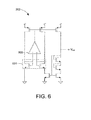
- Fig. 6 depicts a schematic diagram of one embodiment of the voltage reference circuit 202 of Fig. 2 . While the system 200 is described in conjunction with the voltage reference circuit 202 of Fig. 6 , the system 200 may be used in conjunction with any voltage reference circuit 202, according to the principles described herein. Conversely, the voltage reference circuit 202 of Fig. 6 may be used in conjunction with any electronic system and with any other electronic devices or components.
- the voltage reference circuit 202 may include various implementations of the different components.
- the current mirror circuit 104 may include an operational amplifier 600, as shown in Fig. 6 .
- the voltage reference circuit 202 may utilize other components, such as bipolar junction transistors (BJTs), which may include certain characteristics useful for generating the reference voltage 106. As long as the gate-to-substrate and source-to-substrate voltages of the pseudo resistors are equal, respectively, the transistor nonlinearities cancel each other out, and provide resistance characteristics useful for a low-power voltage reference circuit 202.
- BJTs bipolar junction transistors
- Fig. 7 depicts a flowchart diagram of one embodiment of a method 700 for generating a reference voltage 106. Although the method 700 is described in conjunction with the voltage reference circuit 202 of Fig. 3 , the method 700 may be used in conjunction with any type of voltage reference circuit 202.
- the voltage reference circuit 202 is configured to generate 705 a proportional-to-absolute-temperature (PTAT) voltage across the first pseudo resistor 302.
- the first pseudo resistor 302 includes a transistor in the first leg 306 of the current mirror circuit 104.
- the voltage reference circuit 202 then converts 710 the PTAT voltage to a current in the first leg 306 of the current mirror circuit 104 based on a resistance of the first pseudo resistor 302. Because the PTAT voltage is proportional to the temperature, the current is also proportional to the temperature.
- the current mirror circuit 104 copies 715 the current to a second leg 308 of the current mirror circuit 104.
- the current mirror circuit 104 may copy the current to any number of mirrored legs in the current mirror circuit 104, each associated with a separate reference voltage 106 or reference current output by the voltage reference circuit 202.
- the current mirror circuit 104 may be any type of current mirror circuit 104, such as a cascode current mirror.
- at least some of the cascode transistors in the voltage reference circuit 202 are self-biased. Some or all of transistors in the voltage reference circuit 202 may be saturated.
- the self-biasing may be implemented by using bias pseudo resistors to maintain the cascode transistors 104 in saturation.
- the bias pseudo resistors may include a power down input to prevent current flow through the cascode transistors and to power down the voltage reference circuit 202.
- the voltage reference circuit 202 generates 720 a complimentary-to-absolute temperature (CTAT) voltage in the second leg 308 of the current mirror circuit 104.
- CTAT voltage may be generated by a CTAT voltage generator 312 above the second pseudo resistor 304.
- the CTAT voltage generator 312 may include at least one transistor in the second leg 308.
- the voltage reference circuit 202 is configured to set the transistors in the PTAT voltage generator 310 and the CTAT voltage generator 312 to operate in sub-threshold mode.
- the voltage reference circuit 202 generates 725 a reference voltage 106 based on the CTAT voltage, a resistance of the second pseudo resistor 304, and the current copied from the first leg 306 to the second leg 308.
- the second pseudo resistor 304 includes a transistor in the second leg 308 of the current mirror circuit 104.
- the first pseudo resistor 302 and the second pseudo resistor 304 have equal resistance types.
- the gate-to-substrate voltage and source-to-substrate voltage of the transistor of the first pseudo resistor 302 is set equal to the corresponding voltage values of the transistor of the second pseudo resistor 304.
- the transistors of the pseudo resistors may be the same transistor type, such that the transistors have equal threshold voltages, oxide capacitance, and electron mobility.
- the gates for the transistors of the first pseudo resistor 302 and the second pseudo resistor 304 are connected to the reference voltage 106 that is output by the voltage reference circuit 202 corresponding to the second pseudo resistor 304. Biasing the gates of the pseudo resistors with the reference voltage 106 may keep variations in current small and predictable, and may make the reference voltage 106 independent of variations in the supply voltage 300.
- This current includes two components-a forward and a reverse drift of carriers through the channel. If the drain voltage is larger than the source voltage, the forward current component is much larger than the reverse current. This means that the transistor is saturated.
- the exp - V S V T component is approximately 55 times larger than the exp - V D V T component.
- V R ⁇ 1 n ⁇ V T ⁇ ln I D ⁇ 1 ⁇ W 2 / L 2 I D ⁇ 2 ⁇ W 1 / L 1 .
- V out R 2 R 1 ⁇ V T ⁇ ln I D ⁇ 1 ⁇ W 2 / L 2 I D ⁇ 2 ⁇ W 1 / L 1 + 2 ⁇ V GS .
- the resistors of Fig. 1 may be replaced with pseudo resistors that include transistors, despite the nonlinearity of the transistors, since the nonlinearities compensate each other.
- V out V T ⁇ ln ⁇ ⁇ C OX ⁇ 1 ⁇ W R ⁇ 1 / L R ⁇ 1 ⁇ V GS ⁇ 1 - V T ⁇ 2 ⁇ ⁇ C OX ⁇ 2 ⁇ W R ⁇ 2 / L R ⁇ 2 ⁇ V GS ⁇ 1 - V T ⁇ 1 ⁇ V T ⁇ ln I D ⁇ 1 ⁇ W 2 / L 2 I D ⁇ 2 ⁇ W 1 / L 1 + 2 ⁇ V GS
- V out W R ⁇ 1 / L R ⁇ 1 W R ⁇ 2 / L R ⁇ 2 ⁇ V T ⁇ ln I D ⁇ 1 ⁇ W 2 / L 2 I D ⁇ 2 ⁇ W 1 / L 1 + 2 ⁇ V GS .
- the voltage reference circuit 202 may be used to obtain different reference voltages 106 by changing transistor sizes, making additional adjustments to the current mirror circuit 104 and/or introducing additional components into the voltage reference circuit 202.
- the supply voltage 300 may be a negative supply voltage 300 with the voltage reference circuit 202 in complimentary form.
- the voltage reference circuit 202 is shown herein in specific embodiments using certain configurations of CMOS technologies, embodiments using other configurations of CMOS technologies may be used.
- the pseudo resistors may include one or more transistors to obtain the desired resistance for each leg of the current mirror circuit 104. Also, the transistors in the pseudo resistors may be designed to produce specific reference voltages 106 depending on the implementation of the voltage reference circuit 202.
Landscapes
- Engineering & Computer Science (AREA)
- Microelectronics & Electronic Packaging (AREA)
- Physics & Mathematics (AREA)
- Nonlinear Science (AREA)
- Electromagnetism (AREA)
- General Physics & Mathematics (AREA)
- Radar, Positioning & Navigation (AREA)
- Automation & Control Theory (AREA)
- Power Engineering (AREA)
- Control Of Electrical Variables (AREA)
Applications Claiming Priority (1)
| Application Number | Priority Date | Filing Date | Title |
|---|---|---|---|
| US13/607,562 US8836413B2 (en) | 2012-09-07 | 2012-09-07 | Low-power resistor-less voltage reference circuit |
Publications (2)
| Publication Number | Publication Date |
|---|---|
| EP2706426A2 true EP2706426A2 (fr) | 2014-03-12 |
| EP2706426A3 EP2706426A3 (fr) | 2018-01-10 |
Family
ID=49084900
Family Applications (1)
| Application Number | Title | Priority Date | Filing Date |
|---|---|---|---|
| EP13182995.4A Withdrawn EP2706426A3 (fr) | 2012-09-07 | 2013-09-04 | Circuit de référence de tension sans résistance à basse puissance |
Country Status (2)
| Country | Link |
|---|---|
| US (1) | US8836413B2 (fr) |
| EP (1) | EP2706426A3 (fr) |
Cited By (7)
| Publication number | Priority date | Publication date | Assignee | Title |
|---|---|---|---|---|
| US10139849B2 (en) | 2017-04-25 | 2018-11-27 | Honeywell International Inc. | Simple CMOS threshold voltage extraction circuit |
| US10285590B2 (en) | 2016-06-14 | 2019-05-14 | The Regents Of The University Of Michigan | Intraocular pressure sensor with improved voltage reference circuit |
| US10310537B2 (en) | 2016-06-14 | 2019-06-04 | The Regents Of The University Of Michigan | Variation-tolerant voltage reference |
| CN111625046A (zh) * | 2020-06-12 | 2020-09-04 | 深圳市中科创想科技有限责任公司 | 一种可参数修调的低温度系数基准电压源 |
| CN112803895A (zh) * | 2020-12-31 | 2021-05-14 | 上海交通大学 | 一种基于开关电容的伪电阻矫正电路 |
| CN114942664A (zh) * | 2022-06-02 | 2022-08-26 | 广州大学 | 一种皮瓦级宽温度范围的cmos电压基准源 |
| CN117453002A (zh) * | 2023-11-23 | 2024-01-26 | 合肥联诺科技股份有限公司 | 一种片内高精度时钟基准源电路 |
Families Citing this family (15)
| Publication number | Priority date | Publication date | Assignee | Title |
|---|---|---|---|---|
| US9594390B2 (en) | 2014-11-26 | 2017-03-14 | Taiwan Semiconductor Manufacturing Company Limited | Voltage reference circuit |
| EP4212983A1 (fr) * | 2015-05-08 | 2023-07-19 | STMicroelectronics S.r.l. | Circuit pour la génération d'une tension de référence de bande interdite |
| KR102498571B1 (ko) * | 2016-06-02 | 2023-02-15 | 에스케이하이닉스 주식회사 | 기준 전압 생성회로 및 그의 구동 방법 |
| US10250199B2 (en) * | 2016-09-16 | 2019-04-02 | Psemi Corporation | Cascode amplifier bias circuits |
| TWI611659B (zh) * | 2017-02-13 | 2018-01-11 | 華邦電子股份有限公司 | 可調阻值式虛擬電阻 |
| CN108429545B (zh) | 2017-02-13 | 2022-05-31 | 华邦电子股份有限公司 | 可调阻值式虚拟电阻 |
| KR102347178B1 (ko) | 2017-07-19 | 2022-01-04 | 삼성전자주식회사 | 기준 전압 회로를 포함하는 단말 장치 |
| US11233503B2 (en) | 2019-03-28 | 2022-01-25 | University Of Utah Research Foundation | Temperature sensors and methods of use |
| CN113282127B (zh) * | 2021-04-20 | 2024-07-23 | 杭州电子科技大学 | 一种基准电流源 |
| CN113282129B (zh) * | 2021-05-07 | 2024-08-09 | 杭州电子科技大学 | 一种纯场效应管低功耗过温保护电路 |
| CN113741613B (zh) * | 2021-09-26 | 2022-05-17 | 电子科技大学 | 一种零温可调的acot充电电流电路 |
| US12519436B2 (en) * | 2022-06-30 | 2026-01-06 | Cadence Design Systems, Inc. | Referential amplifier devices and methods of use thereof |
| CN115421551A (zh) * | 2022-08-30 | 2022-12-02 | 成都微光集电科技有限公司 | 带隙基准电路及芯片 |
| CN115857607B (zh) * | 2022-11-21 | 2025-03-18 | 重庆邮电大学 | 一种低功耗全mos的自偏置电流基准源 |
| US12111675B1 (en) * | 2024-04-09 | 2024-10-08 | Itu472, Llc | Curvature-corrected bandgap reference |
Family Cites Families (9)
| Publication number | Priority date | Publication date | Assignee | Title |
|---|---|---|---|---|
| US6529066B1 (en) * | 2000-02-28 | 2003-03-04 | National Semiconductor Corporation | Low voltage band gap circuit and method |
| US20090039949A1 (en) * | 2007-08-09 | 2009-02-12 | Giovanni Pietrobon | Method and apparatus for producing a low-noise, temperature-compensated bandgap voltage reference |
| US8072259B1 (en) * | 2008-04-30 | 2011-12-06 | Integrated Device Technology, Inc. | Voltage reference and supply voltage level detector circuits using proportional to absolute temperature cells |
| JP4837111B2 (ja) * | 2009-03-02 | 2011-12-14 | 株式会社半導体理工学研究センター | 基準電流源回路 |
| US8760216B2 (en) * | 2009-06-09 | 2014-06-24 | Analog Devices, Inc. | Reference voltage generators for integrated circuits |
| US8305068B2 (en) * | 2009-11-25 | 2012-11-06 | Freescale Semiconductor, Inc. | Voltage reference circuit |
| EP2360547B1 (fr) * | 2010-02-17 | 2013-04-10 | ams AG | Circuit de référence de bande interdite |
| US8330526B2 (en) * | 2010-07-15 | 2012-12-11 | Freescale Semiconductor, Inc. | Low voltage detector |
| US8432214B2 (en) * | 2011-03-21 | 2013-04-30 | Freescale Semiconductor, Inc. | Programmable temperature sensing circuit for an integrated circuit |
-
2012
- 2012-09-07 US US13/607,562 patent/US8836413B2/en active Active
-
2013
- 2013-09-04 EP EP13182995.4A patent/EP2706426A3/fr not_active Withdrawn
Non-Patent Citations (1)
| Title |
|---|
| None |
Cited By (9)
| Publication number | Priority date | Publication date | Assignee | Title |
|---|---|---|---|---|
| US10285590B2 (en) | 2016-06-14 | 2019-05-14 | The Regents Of The University Of Michigan | Intraocular pressure sensor with improved voltage reference circuit |
| US10310537B2 (en) | 2016-06-14 | 2019-06-04 | The Regents Of The University Of Michigan | Variation-tolerant voltage reference |
| US10139849B2 (en) | 2017-04-25 | 2018-11-27 | Honeywell International Inc. | Simple CMOS threshold voltage extraction circuit |
| CN111625046A (zh) * | 2020-06-12 | 2020-09-04 | 深圳市中科创想科技有限责任公司 | 一种可参数修调的低温度系数基准电压源 |
| CN112803895A (zh) * | 2020-12-31 | 2021-05-14 | 上海交通大学 | 一种基于开关电容的伪电阻矫正电路 |
| CN112803895B (zh) * | 2020-12-31 | 2022-09-02 | 上海交通大学 | 一种基于开关电容的伪电阻矫正电路 |
| CN114942664A (zh) * | 2022-06-02 | 2022-08-26 | 广州大学 | 一种皮瓦级宽温度范围的cmos电压基准源 |
| CN114942664B (zh) * | 2022-06-02 | 2023-09-12 | 广州大学 | 一种皮瓦级宽温度范围的cmos电压基准源 |
| CN117453002A (zh) * | 2023-11-23 | 2024-01-26 | 合肥联诺科技股份有限公司 | 一种片内高精度时钟基准源电路 |
Also Published As
| Publication number | Publication date |
|---|---|
| US8836413B2 (en) | 2014-09-16 |
| EP2706426A3 (fr) | 2018-01-10 |
| US20140070873A1 (en) | 2014-03-13 |
Similar Documents
| Publication | Publication Date | Title |
|---|---|---|
| US8836413B2 (en) | Low-power resistor-less voltage reference circuit | |
| CN114995583B (zh) | 亚带隙补偿参考电压生成电路 | |
| Zhang et al. | A nano-watt MOS-only voltage reference with high-slope PTAT voltage generators | |
| US9436206B2 (en) | Temperature and process compensated current reference circuits | |
| TWI459173B (zh) | 參考電壓產生電路及參考電壓產生方法 | |
| EP3584667B1 (fr) | Circuit de tension de référence de dérive à basse température | |
| US9665116B1 (en) | Low voltage current mode bandgap circuit and method | |
| KR20110019064A (ko) | 전류 기준 회로 | |
| US7999529B2 (en) | Methods and apparatus for generating voltage references using transistor threshold differences | |
| CN103941789B (zh) | 低偏移带隙电路和校正器 | |
| JP2010176258A (ja) | 電圧発生回路 | |
| Basyurt et al. | A 0.4-V supply curvature-corrected reference generator with 84.5-ppm/° C average temperature coefficient within− 40° C to 130° C | |
| TW201308038A (zh) | 帶隙電路 | |
| Nagulapalli et al. | A novel current reference in 45nm cmos technology | |
| US11411494B2 (en) | Reference current source circuit | |
| CN109491433B (zh) | 一种适用于图像传感器的基准电压源电路结构 | |
| Casañas et al. | A review of CMOS currente references | |
| JP4263056B2 (ja) | 基準電圧発生回路 | |
| JP4259941B2 (ja) | 基準電圧発生回路 | |
| JP2013054535A (ja) | 定電圧発生回路 | |
| Campana et al. | 5 V Supply Resistorless Voltage Reference for Low Voltage Applications | |
| Hongprasit et al. | Design of bandgap core and startup circuits for all cmos bandgap voltage reference | |
| Pereira‐Rial et al. | Ultralow power voltage reference circuit for implantable devices in standard CMOS technology | |
| US9024682B2 (en) | Proportional-to-supply analog current generator | |
| de Lima et al. | Performance and variability trade-offs of CMOS PTAT generator topologies for voltage reference applications |
Legal Events
| Date | Code | Title | Description |
|---|---|---|---|
| PUAI | Public reference made under article 153(3) epc to a published international application that has entered the european phase |
Free format text: ORIGINAL CODE: 0009012 |
|
| AK | Designated contracting states |
Kind code of ref document: A2 Designated state(s): AL AT BE BG CH CY CZ DE DK EE ES FI FR GB GR HR HU IE IS IT LI LT LU LV MC MK MT NL NO PL PT RO RS SE SI SK SM TR |
|
| AX | Request for extension of the european patent |
Extension state: BA ME |
|
| 17P | Request for examination filed |
Effective date: 20140326 |
|
| PUAL | Search report despatched |
Free format text: ORIGINAL CODE: 0009013 |
|
| AK | Designated contracting states |
Kind code of ref document: A3 Designated state(s): AL AT BE BG CH CY CZ DE DK EE ES FI FR GB GR HR HU IE IS IT LI LT LU LV MC MK MT NL NO PL PT RO RS SE SI SK SM TR |
|
| AX | Request for extension of the european patent |
Extension state: BA ME |
|
| RIC1 | Information provided on ipc code assigned before grant |
Ipc: G05F 3/24 20060101AFI20171201BHEP Ipc: G05F 3/30 20060101ALI20171201BHEP |
|
| STAA | Information on the status of an ep patent application or granted ep patent |
Free format text: STATUS: REQUEST FOR EXAMINATION WAS MADE |
|
| STAA | Information on the status of an ep patent application or granted ep patent |
Free format text: STATUS: THE APPLICATION IS DEEMED TO BE WITHDRAWN |
|
| 18D | Application deemed to be withdrawn |
Effective date: 20180711 |