EP2709017B1 - Dispositif pour contrôler l'accès à une structure d'antémémoire - Google Patents
Dispositif pour contrôler l'accès à une structure d'antémémoire Download PDFInfo
- Publication number
- EP2709017B1 EP2709017B1 EP12184447.6A EP12184447A EP2709017B1 EP 2709017 B1 EP2709017 B1 EP 2709017B1 EP 12184447 A EP12184447 A EP 12184447A EP 2709017 B1 EP2709017 B1 EP 2709017B1
- Authority
- EP
- European Patent Office
- Prior art keywords
- cache
- bits
- access
- address
- module
- Prior art date
- Legal status (The legal status is an assumption and is not a legal conclusion. Google has not performed a legal analysis and makes no representation as to the accuracy of the status listed.)
- Active
Links
Images
Classifications
-
- G—PHYSICS
- G06—COMPUTING OR CALCULATING; COUNTING
- G06F—ELECTRIC DIGITAL DATA PROCESSING
- G06F12/00—Accessing, addressing or allocating within memory systems or architectures
- G06F12/02—Addressing or allocation; Relocation
- G06F12/08—Addressing or allocation; Relocation in hierarchically structured memory systems, e.g. virtual memory systems
- G06F12/0802—Addressing of a memory level in which the access to the desired data or data block requires associative addressing means, e.g. caches
- G06F12/0864—Addressing of a memory level in which the access to the desired data or data block requires associative addressing means, e.g. caches using pseudo-associative means, e.g. set-associative or hashing
-
- G—PHYSICS
- G06—COMPUTING OR CALCULATING; COUNTING
- G06F—ELECTRIC DIGITAL DATA PROCESSING
- G06F12/00—Accessing, addressing or allocating within memory systems or architectures
- G06F12/14—Protection against unauthorised use of memory or access to memory
- G06F12/1408—Protection against unauthorised use of memory or access to memory by using cryptography
Definitions
- the present invention relates to a method for controlling the access to a cache structure comprising multiple cache sets during the execution of at least one computer program. More specifically, the invention relates to a method capable of guaranteeing that each address accessed by a computer program can be attached a true probability to be allocated to any particular cache set of a cache structure.
- the invention also relates to a device and a computer program product for controlling the access to a cache structure suitable for carrying out such a method.
- the invention may be applied to real-time systems, for example safety-critical real-time systems such as flight control systems.
- Caches are generally small, fast storage buffers employable to store information, such as code or data, in order for a program running in a processing device to execute faster. Typically, it is faster for the processing device to read the cache than to read a main memory. Also, with the rapid increase of intensive computational requirements, their importance in a computing system will only increase.
- a cache structure is conceptually a matrix of S*W cache lines (conceptually cells) arranged in S sets (conceptually rows) and W ways (conceptually columns).
- the set (that is, the row) in which a piece of data is placed into cache is determined by the placement policy .
- the placement policy implements a hash function that uses certain bits of the memory address in which the piece of data is stored to map that piece of data into a specific cache set (row). From the point of view of the cache, different pieces of data can be grouped into cache lines, or simply lines. Since different memory lines can collide into the same cache set, cache sets consist of a given number of cache lines called ways (that is, columns). All sets have the same number of ways, which determine the associativity of the cache.
- a W-way set-associative cache comprises W ways per set.
- the way (cache line) in which a memory line is placed is determined by the replacement policy.
- the replacement policy selects, among all the ways (columns) in a given set (row), which memory line is evicted to make room for the new memory line.
- the new memory line is then stored in the cache line whose contents (a memory line) have been just evicted.
- Each line can be composed by one or several words. The granularity of a word is usually measured in bytes (e.g. 1, 2 or 4 bytes).
- the timing behaviour of a cache is mainly determined by its placement and replacement policies.
- the line size, the word size and other cache parameters may also affect the timing behaviour of the cache. For a given cache configuration both, line size and word size, are fixed.
- Randomised caches in high-performance processors have been proposed to remove cache conflicts by using pseudo-random hash functions [ A. Gonzalez et al. Eliminating cache conflict misses through XOR-based placement functions. In ICS, 1997 .][ A. Seznec and F. Bodin. Skewed-associative caches. In PARLE. 1993 .][ Nigel Topham and Antonio González. Randomized cache placement for eliminating conflicts. IEEE Trans. Comput., 48, February 1999 ].
- the behaviour of all those cache designs is fully deterministic. This means that, whenever a given data input set for a program makes that program to generate a pathological access pattern, this pattern will repeat systematically for such input set in all runs of the program. Therefore, although the frequency of pathological cases is reduced, they can still appear systematically because there is no way to prove that their probability is bound.
- Random replacement policies exist to make random the selection of a cache line (cell) inside a cache set (row).
- existing placement policies are purely deterministic based on the address accessed. Therefore, whether accesses to two different addresses compete for the same cache set depends solely on their particular addresses and the placement function used. Hence, if two addresses are placed into the same cache set at the beginning of the execution, they will collide in that cache set always during the execution of the program and across all runs of the program. Since the behaviour is purely deterministic no true probability can be computed. Hence, the probabilistic properties required by Probabilistic Timing Analysis (PTA) are not fulfilled.
- PTA Probabilistic Timing Analysis
- the invention provides a device for controlling the access to a cache structure comprising multiple cache sets during the execution of at least one computer program, the device comprising a module for generating seed values during the execution of the at least one computer program; a parametric hash function module for generating a cache set identifier to access the cache structure, the identifier being generated by combining a seed value generated by the module for generating seed values and predetermined bits of an address to access a main memory associated to the cache structure.
- the provision of the seed value guarantees a given access having true probabilities to be assigned to each of the cache sets of the cache structure regardless of the value of the address. That is, the invention is capable of guaranteeing that each address accessed by a computer program, through a processor module such as a microprocessor, can be attached a true probability to be allocated to any particular cache set of a cache structure comprising multiple sets.
- the generated seed value may be updated either periodically or whenever a particular event occurs.
- the seed value may be updated only at the beginning or the end of the execution of the computer program, although updating it at a different time, or with higher or lower frequency is also within the scope of the invention.
- any parametric hash function module may be used as long as there is a real probability that an address may be mapped to any set. Any seed value may be used. However, a higher degree of randomisation is achieved if the parametric hash function module produces large variations in its output set identifier even if small changes occur in the input address and/or the seed value, and if the seed is set to a random or pseudo-random value.
- cache structures with multiple sets implementing placement functions are more convenient in terms of energy. Those cache structures with multiple sets are known as direct-mapped caches if they have only one cache line per set (no replacement policy needed) and as set-associative caches if they have more than one cache line per set (both placement and replacement policies needed).
- the cache structure may comprise 2 n sets, and the generated cache set identifier may comprise n bits.
- the given address comprises a sequence of bits, a subset of them that may correspond to an offset, and the predetermined set-identifier bits of the address may comprise the sequence of bits without the offset.
- the cache structure may comprise at least one cache line per set, such as a set-associative cache structure or a direct-mapped cache structure.
- the module for generating seed values during the execution of at least one computer program may comprise a pseudo-random number generator, which may be implemented either in hardware or in software.
- the module for generating seed values may be implemented in hardware by means of electronic elements (e.g. logic gates).
- the device may comprise a memory module for storing the generated seed values, so that all the generated seed values may be stored in the memory module. Alternatively, every newly generated seed value may replace the previously generated seed value.
- the invention provides a method of controlling the access to a cache structure comprising multiple cache sets during the execution of at least one computer program, the method comprising:
- a computer program product comprising program instructions for causing a computer to perform the method of controlling the access to a cache structure as described above.
- the invention also relates to such a computer program product embodied on a storage medium (for example, a CD-ROM, a DVD, a USB drive, on a computer memory or on a read-only memory) or carried on a carrier signal (for example, on an electrical or optical carrier signal).
- the invention also provides a cache structure comprising multiple cache sets and the device for controlling the access to the cache structure as described above.
- Execution of computer programs in a computer system relates to the process by which the computer system, through its processor, carries out the instructions of the computer program. Some of these instructions may need to access data stored in a predetermined address of a main memory comprised in the computer system. This way, when the processor tries to access the main memory according to the predetermined address for obtaining the needed data, firstly it verifies if the required data is stored in a cache structure associated to the main memory. This is the reason why a cache structure comprises generally small, fast storage buffers employable to store information, which allows a processor to more quickly and efficiently have access to the information, that is, it is faster for a processor to read the smaller memory of a cache structure than to read a main memory.
- a cache structure is conceptually a matrix of S*W cache lines (conceptually cells) arranged in S sets (conceptually rows) and W ways (conceptually columns).
- the set that is, the row
- the placement policy implements a hash function that uses certain bits of the memory address to map each particular memory line into a specific cache set (row). Since different memory lines can collide into the same cache set, cache sets consist of a given number of lines called ways (that is, columns). All sets have the same number of ways, which determine the associativity of the cache.
- a W-way set-associative cache comprises W ways per set.
- the way (cache line) in which a memory line is placed is determined by the replacement policy.
- the replacement policy selects, among all the ways (columns) in a given set (row), which memory line is evicted to make room for the new memory line.
- the new memory line is then stored in the cache line whose contents (a memory line) have been just evicted.
- Each line can be composed by one or several words. The granularity of a word is usually measured in bytes (e.g. 1, 2 or 4 bytes).
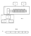
- FIG. 1 illustrates a processor setup in which a cache structure 10 is deployed.
- the cache structure 10 comprising a plurality of ways W1-W8 and a plurality of sets S1-S4 (that is, a matrix of 4*8 cache lines).
- the cache structure 10 is coupled to a central processing unit (CPU) 11 and a main memory 12.
- the cache structure 10 also comprises a set placement logic module 13 that determines which set of the cache sets S1-S4 is used to allocate a given address to access the main memory 12, issued from the CPU 11.
- the set placement logic module 13 receives the cache set identifier to access the cache structure 10 from a device 14 for controlling the access to the cache structure according to the invention.
- the controlling device 14 comprises a parametric hash function module 15 that combines a seed value 16 generated by, for example, a pseudo-random number generator (not shown) and predetermined bits 17 of the given address to access the main memory 12.
- pseudo-random number generator may be implemented either in hardware or in software, although any other way to obtain the seed value is within the scope of the invention.
- the invention also proposes updating the seed value 16 only at the beginning or the end of the execution of the computer program, although updating it at a different time, or with higher or lower frequency is also within the scope of the invention.
- Any parametric hash function module may be used as long as there is a real probability that an address may be mapped to any set. Any seed value may be used. However, PTA results are better (lower execution times) if the parametric hash function module produces large variations in its output set identifier even if small changes occur in the input address and/or the seed value, and if the seed is set to a random or pseudo-random value.
- controlling device 14 can also comprise a register (not shown) for storing the generated seed value 16.
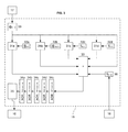
- Figure 2 illustrates an example of an address 20 to access the main memory 12, issued from the CPU 11, predetermined bits 17 of which are combined with the seed value 16 for obtaining the cache set identifier to access the cache structure 10.
- the address 20 comprises three parts of bits:
- addresses are 16-bit wide and the cache line size is 64 bytes (2 6 bytes - in general, the number of bytes is 2 n ) then, for the cache structure shown in Figure 1 (4 sets S1-S4, 8 ways W1-W8), the address bits are classified as follows: the 8 uppermost bits are the tag 21; the following 2 bits (that is, given that the cache comprises 4 sets it requires 2 bits for addressing all sets) are the index 22; and the 6 (that is "n") lowermost bits are the offset 23. In this way, if the address is "0011 0011 0100 0111" (in binary) the tag 21 is "0011 0011", the index 22 is "01”, and the offset 23 is "00 0111".
- Conventional placement policies use the index 22 ("01" in the example) to choose the cache set accessed by providing those bits to the set placement logic module 13.
- the set S1 is accessed if the index bits are "00"; the set S2 is accessed if the index bits are "01" (as in the example); the set S3 is accessed if the index bits are "10”; and the set S4 is accessed if the index bits are "11".
- Other placement policies are known that combine tag 21 and index 22 bits to generate a cache set identifier. However, clearly these placement policies are deterministic since the generated cache set identifier depends solely on the address accessed.
- the device 14 combines the bits of the tag 21 and the index 22 (that is, the predetermined bits 17 of the address 20) and the seed value 16 to generate a cache set identifier by means of the parametric hash function module 15.
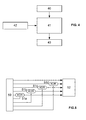
- Figure 3 shows an embodiment of a parametric hash function module 15.
- the combination of the seed value 16 and the predetermined bits 17 of the address 20 i.e. in the present embodiment, the tag 21 and the index 22
- the seed value 16 and the predetermined bits 17 of the address 20 can be performed in different ways with the purpose of generating a cache set identifier to access the cache structure, whence the parametric hash function module 15 can have different settings.
- the parametric hash function module 15 comprises a register 30 for receiving and storing the predetermined bits 17 of the address 20. Because in the present embodiment the address has 32 bits, the predetermined bits of the address are the bits 5 to 31 of the address (i.e. the address 20 without the offset 23).
- the parametric hash function module 15 also comprises a register 36 for receiving and storing the seed value 16 (in the present embodiment the seed value comprises 32 bits); a plurality of modules 31a,31b,31c,31d for rotating the predetermined bits 17 of the address 20 based either on some bits 32a,32b,32c,32d of the seed value 16 or some bits of the predetermined bits 17; a module 33 for concatenating the bits of the seed value 16, the predetermined bits 17 of the address 20, and the bits obtained in the output of each rotating module 31a,31b,31c,31d; and a plurality of XOR-folding logic modules 34a,34b,34c,34d,34e of different lengths for adapting the number of bits of the concatenated binary value to a binary value having as many bits as needed to index all cache sets.
- the seed value comprises 32 bits
- modules 31a,31b,31c,31d for rotating the predetermined bits 17 of the address 20 based either on some bits 32a,32b,32c
- the output of the XOR-folding logic module 34a corresponds to the cache set identifier and it is received by a register 35, which provides the identifier to the set placement logic module 13 to access the cache structure 10 and to obtain or input data in the cache set.
- the set placement logic module 13 determines which set of the cache sets S1-S4 is used to allocate the given address 20.
- each rotating module comprises a rotate logic element 41 whose object is to rotate a binary value stored in a value register 40 to the left by N positions, where N is determined by a control register 42.
- the output of the rotate logic element 41 is received and stored in a register 43. Therefore, the N leftmost bits of the binary value in the value register 40 become the N rightmost bits of the output register 43 and the remaining M rightmost bits of the binary value in the value register 40 become the M leftmost bits of the output register 43.
- the number of bits of the binary value is a power of two (e.g.
- control register 42 has as many bits as the base-2 logarithm of the size of the binary value. For instance, if the binary value is 32-bits wide, the control register 42 should have 5 bits so that it can take 32 different values that can produce the 32 different rotations of the binary value (from 0 to 31 bit rotation).
- the following example illustrates how a rotating module 31a;31b;31c;31d works. If the binary value is 00110111 (in binary) and the control register 42 is 101, then the output register 43 will be 11100110.
- the control register 42 makes the binary value to be rotated 5 (101 in binary) positions left so that the 5 leftmost bits of the binary value (00110) become the 5 rightmost bits of the binary value stored in the output register 43 and the remaining rightmost 3 bits of the binary value (111) become the 3 leftmost bits of the binary value stored in the output register 43.
- one of the inputs for all rotating modules 31a,31b,31c,31d are the bits of the address 20 discarding offset bits 23.
- Each rotating module uses a different set of bits as a control register 32a;32b;32c;32d. These bits are used to determine how many positions the binary value (i.e. the predetermined bits 17 of the address 20 extended with 5 bits in the left whose value is 00000) is rotated.
- the leftmost rotating module 31 a uses the 5 lowermost bits of the address 20 after discarding the offset. In other words, it uses the 5 rightmost bits of the tag 21 and index 22 pair (bits in position 0, 1, 2, 3, 4 counting from right to left).
- the second leftmost rotating module 31 b uses the next 5 lowermost bits of the tag 21 and index 22 pair (bits in position from 5 to 9).
- the other two rotating modules 31c,31d use bits from the seed value 16. In particular, they use bits 0 to 4 and bits 5 to 9, respectively.
- XOR modules 34a,34b,34c,34d,34e are applied in cascaded fashion to the output of the concatenating module 33 until the binary value has as many bits as needed to index all cache sets. Consequently, the XOR modules allow reducing the number of bits of the binary value until the binary value has as many bits as needed to index all cache sets.
- the XOR module is configured for the case in which the binary value has 9 bits though its functioning is the same regardless of the number of bits of the binary value used as input.
- the XOR module splits the bits of the binary value stored in a first register 50 into two halves and it carries out a XOR operation 51 a,51 b,51 c,51 d between each pair of bits in symmetric positions in each of the halves, i.e. XOR between bits 0 and 7, bits 1 and 6, bits 2 and 5; and bits 3 and 4. If the number of bits is odd, then the uppermost bit is simply propagated to the output (this is the case shown in Figure 5 ).
- the XOR operation with 2 input bits produces a "1” if input bits differ (i.e. one of them is “0” and the other one is “1 ”) and a "0” if they match (both of them are either "0” or "1 ").
- the binary value obtained is stored in the output register 52.
- the binary value of the concatenation provided by the concatenating module 33 has 200 bits and the number of cache sets is 32, we must XOR those 200 bits until having only 5 bits to index all cache sets (5 is the base-2 logarithm of 32). Therefore, different levels of XOR modules will reduce the number of bits from 200 to 100, from 100 to 50, from 50 to 25, from 25 to 13, from 13 to 7, and from 7 to 5.
- the XOR logic is applied only for as many pairs of bits as the number of input bits (7 in the example) minus the number of output bits required (5 in the example), which means that is applied over 2 pair of bits. For that purpose, as many bits as needed are simply propagated from the left side of the input (3 bits in this case) and the remaining bits (4 bits in the example) are XOR-folded so that it is obtained as output those bits propagated (3 bits) and the output of XORing the pairs (2 bits).
- the first XOR module 34e receives a 187-bit binary value (as described above) from the concatenating module 33 and transforms it in a 94-bit binary value.
- the second XOR module 34d receives and transforms said 94-bit binary value into a 47-bit binary value.
- Said output value is received by the third XOR module 34c, which transforms the 47-bit binary value into a 24-bit binary value.
- Said 24-bit binary value is received by the fourth XOR module 34b, which transforms it into a 12-bit binary value.
- the 12-bit binary value is sent to the fifth XOR module 34a that transforms it into a value having as many bits as needed to index all cache sets of the cache structure. Once the appropriate value is obtained, it is stored in the output register 35, which provides the binary value to the set placement logic module 13 to access the cache structure 10.
- the invention is not limited to any of those decisions and any other parametric hash function module 15 using rotating modules, XOR modules or any other kind of logic fall within the scope of the invention as long as the inputs of the parametric hash function module includes the address and a seed.
- the embodiments of the invention described with reference to the drawings comprise computer apparatus and processes performed in computer apparatus, the invention also extends to computer programs, particularly computer programs on or in a carrier, adapted for putting the invention into practice.
- the program may be in the form of source code, object code, a code intermediate source and object code such as in partially compiled form, or in any other form suitable for use in the implementation of the processes according to the invention.
- the carrier may be any entity or device capable of carrying the program.
- the carrier may comprise a storage medium, such as a ROM, for example a CD ROM or a semiconductor ROM, or a magnetic recording medium, for example a floppy disc or hard disk.
- a storage medium such as a ROM, for example a CD ROM or a semiconductor ROM, or a magnetic recording medium, for example a floppy disc or hard disk.
- the carrier may be a transmissible carrier such as an electrical or optical signal, which may be conveyed via electrical or optical cable or by radio or other means.
- the carrier may be constituted by such cable or other device or means.
- the carrier may be an integrated circuit in which the program is embedded, the integrated circuit being adapted for performing, or for use in the performance of, the relevant processes.
Landscapes
- Engineering & Computer Science (AREA)
- Theoretical Computer Science (AREA)
- Physics & Mathematics (AREA)
- General Engineering & Computer Science (AREA)
- General Physics & Mathematics (AREA)
- Memory System Of A Hierarchy Structure (AREA)
- Image Processing (AREA)
Claims (11)
- Un dispositif pour contrôler l'accès à une structure d'antémémoire comprenant des multiples ensembles d'antémémoire pendant l'exécution d'au moins un programme informatique, comprenant le dispositif :- un module de génération des valeurs initiales aléatoires ou pseudo-aléatoires pendant l'exécution du au moins un programme informatique ;- un module de fonction de hachage paramétrique pour générer un identificateur d'ensemble d'antémémoire pour l'accès à la structure d'antémémoire, étant généré l'identificateur en combinant une valeur initiale générée para le module de génération des valeurs initiales et des bits prédéterminés d'une adresse pour accéder à une mémoire principale associée à la structure d'antémémoire.
- Le dispositif selon la revendication 1, dans lequel la structure d'antémémoire comprend 2n ensembles, et dans lequel l'identificateur d'ensemble d'antémémoire généré comprend n bits.
- Le dispositif selon l'une quelconque des revendications 1 ou 2, dans lequel l'adresse donnée comprend une séquence de bits, dont une partie correspond à un offset, et dans lequel les bits prédéterminés de l'adresse comprennent la séquence de bits sans l'offset.
- Le dispositif selon l'une quelconque des revendications 1 à 3, dans lequel la structure d'antémémoire comprend au moins une ligne d'antémémoire par ensemble.
- Le dispositif selon l'une quelconque des revendications 1 à 4, dans lequel le module de génération de valeurs initiales comprend un générateur de nombres pseudo-aléatoires.
- Le dispositif selon l'une quelconque des revendications 1 à 5, comprenant en outre un module de mémoire pour stocker les valeurs initiales générées.
- Un procédé pour contrôler l'accès à une structure d'antémémoire comprenant des multiples ensembles d'antémémoire pendant l'exécution d'au moins un programme informatique, comprenant le procédé :- générer des valeurs initiales aléatoires ou pseudo-aléatoires pendant l'exécution du au moins un programme informatique ;- recevoir une adresse pour accéder à une mémoire principale associée à la structure d'antémémoire ;- générer un identificateur d'ensemble d'antémémoire pour accéder à la structure d'antémémoire, étant généré l'identificateur en combinant une valeur initiale générée et des bits prédéterminés de l'adresse reçue.
- Produit de programme informatique comprenant des instructions de programme pour faire qu'un ordinateur exécute un procédé pour contrôler l'accès à une structure d'antémémoire comprenant des multiples ensembles d'antémémoire selon la revendication 7.
- Produit de programme informatique selon la revendication 8, incorporé dans un support de stockage.
- Produit de programme informatique selon la revendication 8, porté dans un signal porteur.
- Une structure d'antémémoire comprenant des multiples ensembles d'antémémoire et le dispositif pour contrôler l'accès à la structure d'antémémoire selon l'une quelconque des revendications 1 à 6.
Priority Applications (5)
| Application Number | Priority Date | Filing Date | Title |
|---|---|---|---|
| EP12184447.6A EP2709017B1 (fr) | 2012-09-14 | 2012-09-14 | Dispositif pour contrôler l'accès à une structure d'antémémoire |
| ES12184447.6T ES2546072T3 (es) | 2012-09-14 | 2012-09-14 | Dispositivo para controlar el acceso a una estructura de memoria caché |
| JP2013189544A JP2014059871A (ja) | 2012-09-14 | 2013-09-12 | キャッシュ構造へのアクセスを制御するための装置 |
| CN201310418254.0A CN103823763B (zh) | 2012-09-14 | 2013-09-13 | 用于控制对缓存结构的访问的装置 |
| US14/026,925 US9396119B2 (en) | 2012-09-14 | 2013-09-13 | Device for controlling the access to a cache structure |
Applications Claiming Priority (1)
| Application Number | Priority Date | Filing Date | Title |
|---|---|---|---|
| EP12184447.6A EP2709017B1 (fr) | 2012-09-14 | 2012-09-14 | Dispositif pour contrôler l'accès à une structure d'antémémoire |
Publications (2)
| Publication Number | Publication Date |
|---|---|
| EP2709017A1 EP2709017A1 (fr) | 2014-03-19 |
| EP2709017B1 true EP2709017B1 (fr) | 2015-05-27 |
Family
ID=46845625
Family Applications (1)
| Application Number | Title | Priority Date | Filing Date |
|---|---|---|---|
| EP12184447.6A Active EP2709017B1 (fr) | 2012-09-14 | 2012-09-14 | Dispositif pour contrôler l'accès à une structure d'antémémoire |
Country Status (5)
| Country | Link |
|---|---|
| US (1) | US9396119B2 (fr) |
| EP (1) | EP2709017B1 (fr) |
| JP (1) | JP2014059871A (fr) |
| CN (1) | CN103823763B (fr) |
| ES (1) | ES2546072T3 (fr) |
Families Citing this family (18)
| Publication number | Priority date | Publication date | Assignee | Title |
|---|---|---|---|---|
| US9367456B1 (en) * | 2013-06-14 | 2016-06-14 | Marvell International Ltd. | Integrated circuit and method for accessing segments of a cache line in arrays of storage elements of a folded cache |
| US9652397B2 (en) * | 2014-04-23 | 2017-05-16 | Texas Instruments Incorporated | Dynamic power reduction and performance improvement in caches using fast access |
| CN105814548B (zh) * | 2014-07-14 | 2019-02-12 | 上海兆芯集成电路有限公司 | 具有使用不同编索引方案的主高速缓存器和溢出高速缓存器的高速缓存器系统 |
| US10089238B2 (en) * | 2014-07-17 | 2018-10-02 | Qualcomm Incorporated | Method and apparatus for a shared cache with dynamic partitioning |
| EP3195178B1 (fr) | 2014-07-23 | 2019-02-20 | GrammaTech, Inc. | Systèmes et/ou procédés pour une protection automatique contre les vulnérabilités dues aux corruptions de mémoire |
| GB2530722B (en) | 2014-09-19 | 2016-08-17 | Imagination Tech Ltd | Cache hashing |
| WO2016055828A1 (fr) * | 2014-10-08 | 2016-04-14 | Via Alliance Semiconductor Co., Ltd. | Système de cache avec cache primaire et cache fifo de trop-plein |
| DE102015205827A1 (de) | 2015-03-31 | 2016-10-06 | Siemens Aktiengesellschaft | Verfahren zum Schutz sicherheitsrelevanter Daten in einem Cachespeicher |
| US9846648B2 (en) * | 2015-05-11 | 2017-12-19 | Intel Corporation | Create page locality in cache controller cache allocation |
| CN105335520B (zh) * | 2015-11-24 | 2018-11-16 | 交控科技股份有限公司 | 一种基于地铁综合自动化系统的数据处理方法及处理器 |
| GB2546731B (en) * | 2016-01-20 | 2019-02-20 | Advanced Risc Mach Ltd | Recording set indicator |
| GB2542646B (en) | 2016-03-18 | 2017-11-15 | Imagination Tech Ltd | Non-linear cache logic |
| GB2560336B (en) * | 2017-03-07 | 2020-05-06 | Imagination Tech Ltd | Address generators for verifying integrated circuit hardware designs for cache memory |
| US11010288B2 (en) | 2019-07-31 | 2021-05-18 | Micron Technology, Inc. | Spare cache set to accelerate speculative execution, wherein the spare cache set, allocated when transitioning from non-speculative execution to speculative execution, is reserved during previous transitioning from the non-speculative execution to the speculative execution |
| US11200166B2 (en) | 2019-07-31 | 2021-12-14 | Micron Technology, Inc. | Data defined caches for speculative and normal executions |
| US11194582B2 (en) | 2019-07-31 | 2021-12-07 | Micron Technology, Inc. | Cache systems for main and speculative threads of processors |
| US11048636B2 (en) * | 2019-07-31 | 2021-06-29 | Micron Technology, Inc. | Cache with set associativity having data defined cache sets |
| US12019563B2 (en) * | 2020-09-25 | 2024-06-25 | Intel Corporation | Cache set permutations based on Galois Field operations |
Family Cites Families (14)
| Publication number | Priority date | Publication date | Assignee | Title |
|---|---|---|---|---|
| US5649143A (en) * | 1995-06-02 | 1997-07-15 | Sun Microsystems, Inc. | Apparatus and method for providing a cache indexing scheme less susceptible to cache collisions |
| US6275919B1 (en) * | 1998-10-15 | 2001-08-14 | Creative Technology Ltd. | Memory storage and retrieval with multiple hashing functions |
| JP2003051819A (ja) * | 2001-08-08 | 2003-02-21 | Toshiba Corp | マイクロプロセッサ |
| GB2412987B (en) * | 2002-04-15 | 2005-12-21 | Hewlett Packard Co | A programmable microprocessor cache index hashing function |
| US20050259819A1 (en) * | 2002-06-24 | 2005-11-24 | Koninklijke Philips Electronics | Method for generating hashes from a compressed multimedia content |
| US7606994B1 (en) * | 2004-11-10 | 2009-10-20 | Sun Microsystems, Inc. | Cache memory system including a partially hashed index |
| US7373480B2 (en) * | 2004-11-18 | 2008-05-13 | Sun Microsystems, Inc. | Apparatus and method for determining stack distance of running software for estimating cache miss rates based upon contents of a hash table |
| US7366871B2 (en) * | 2004-11-18 | 2008-04-29 | Sun Microsystems, Inc. | Apparatus and method for determining stack distance including spatial locality of running software for estimating cache miss rates based upon contents of a hash table |
| US20060206706A1 (en) * | 2005-03-14 | 2006-09-14 | Bryan Dietz | Method and apparatus for dynamically distributing data flow in a communication network |
| US7487397B2 (en) * | 2005-10-27 | 2009-02-03 | International Business Machines Corporation | Method for cache correction using functional tests translated to fuse repair |
| US7937535B2 (en) * | 2007-02-22 | 2011-05-03 | Arm Limited | Managing cache coherency in a data processing apparatus |
| US7743200B1 (en) * | 2007-05-24 | 2010-06-22 | Juniper Networks, Inc. | Instruction cache using perfect hash function |
| US7979640B2 (en) * | 2008-07-28 | 2011-07-12 | Oracle America, Inc. | Cache line duplication in response to a way prediction conflict |
| US8055848B2 (en) * | 2008-07-31 | 2011-11-08 | Samsung Electronics Co., Ltd. | Method and system for securing instruction caches using substantially random instruction mapping scheme |
-
2012
- 2012-09-14 EP EP12184447.6A patent/EP2709017B1/fr active Active
- 2012-09-14 ES ES12184447.6T patent/ES2546072T3/es active Active
-
2013
- 2013-09-12 JP JP2013189544A patent/JP2014059871A/ja active Pending
- 2013-09-13 CN CN201310418254.0A patent/CN103823763B/zh active Active
- 2013-09-13 US US14/026,925 patent/US9396119B2/en active Active
Also Published As
| Publication number | Publication date |
|---|---|
| CN103823763B (zh) | 2018-08-28 |
| US9396119B2 (en) | 2016-07-19 |
| CN103823763A (zh) | 2014-05-28 |
| EP2709017A1 (fr) | 2014-03-19 |
| ES2546072T3 (es) | 2015-09-18 |
| US20140082284A1 (en) | 2014-03-20 |
| JP2014059871A (ja) | 2014-04-03 |
Similar Documents
| Publication | Publication Date | Title |
|---|---|---|
| EP2709017B1 (fr) | Dispositif pour contrôler l'accès à une structure d'antémémoire | |
| Vila et al. | Theory and practice of finding eviction sets | |
| Seong et al. | Security refresh: Prevent malicious wear-out and increase durability for phase-change memory with dynamically randomized address mapping | |
| Zhang et al. | Fork path: improving efficiency of oram by removing redundant memory accesses | |
| US11409663B2 (en) | Methods and systems for optimized translation of a virtual address having multiple virtual address portions using multiple translation lookaside buffer (TLB) arrays for variable page sizes | |
| Zhang et al. | Side channel vulnerability metrics: the promise and the pitfalls | |
| JP2017503299A (ja) | モードに応じてセットの1つ又は複数を選択的に選択するように動的に構成可能であるマルチモード・セット・アソシエイティブ・キャッシュ・メモリ | |
| US8935775B2 (en) | Method and apparatus for dishonest hardware policies | |
| Giner et al. | Scatter and split securely: Defeating cache contention and occupancy attacks | |
| Swami et al. | ACME: Advanced counter mode encryption for secure non-volatile memories | |
| EP3220276B1 (fr) | Logique de cache non linéaire | |
| CN105446897B (zh) | 高速缓存逻辑器、存储器系统及生成高速缓存地址的方法 | |
| KR20100011897A (ko) | 캐시 디렉터리의 실제 페이지 번호 비트의 테스트 | |
| Xu et al. | FusedCache: A naturally inclusive, racetrack memory, dual-level private cache | |
| US12001346B2 (en) | Device, method and system to supplement a skewed cache with a victim cache | |
| EP4002131B1 (fr) | Mémoire séquestrée pour le stockage sélectif de métadonnées correspondant à des données mises en cache | |
| Wang et al. | Self-reinforcing memoization for cryptography calculations in secure memory systems | |
| EP4020233A1 (fr) | Rééquilibrage automatisé d'un ensemble de mémoire cache de traduction d'adresses | |
| Bao et al. | Reducing timing side-channel information leakage using 3D integration | |
| Ramkrishnan et al. | New attacks and defenses for randomized caches | |
| Lipp | Cache attacks on arm | |
| Shafi et al. | Freqcounter: Efficient cacheability of encryption and integrity tree counters in secure processors | |
| Wang | Bo-tree: a dynamic merkle tree for enabling scalable memories | |
| Mangard | Cache Attacks and Rowhammer on ARM | |
| Li et al. | Feasibility Analysis and Performance Optimization of the Conflict Test Algorithms for Searching Eviction Sets |
Legal Events
| Date | Code | Title | Description |
|---|---|---|---|
| PUAI | Public reference made under article 153(3) epc to a published international application that has entered the european phase |
Free format text: ORIGINAL CODE: 0009012 |
|
| AK | Designated contracting states |
Kind code of ref document: A1 Designated state(s): AL AT BE BG CH CY CZ DE DK EE ES FI FR GB GR HR HU IE IS IT LI LT LU LV MC MK MT NL NO PL PT RO RS SE SI SK SM TR |
|
| AX | Request for extension of the european patent |
Extension state: BA ME |
|
| 17P | Request for examination filed |
Effective date: 20140919 |
|
| RBV | Designated contracting states (corrected) |
Designated state(s): AL AT BE BG CH CY CZ DE DK EE ES FI FR GB GR HR HU IE IS IT LI LT LU LV MC MK MT NL NO PL PT RO RS SE SI SK SM TR |
|
| RIC1 | Information provided on ipc code assigned before grant |
Ipc: G06F 12/14 20060101ALN20141030BHEP Ipc: G06F 12/08 20060101AFI20141030BHEP |
|
| GRAP | Despatch of communication of intention to grant a patent |
Free format text: ORIGINAL CODE: EPIDOSNIGR1 |
|
| RIC1 | Information provided on ipc code assigned before grant |
Ipc: G06F 12/14 20060101ALN20141124BHEP Ipc: G06F 12/08 20060101AFI20141124BHEP |
|
| INTG | Intention to grant announced |
Effective date: 20141217 |
|
| GRAS | Grant fee paid |
Free format text: ORIGINAL CODE: EPIDOSNIGR3 |
|
| GRAA | (expected) grant |
Free format text: ORIGINAL CODE: 0009210 |
|
| AK | Designated contracting states |
Kind code of ref document: B1 Designated state(s): AL AT BE BG CH CY CZ DE DK EE ES FI FR GB GR HR HU IE IS IT LI LT LU LV MC MK MT NL NO PL PT RO RS SE SI SK SM TR |
|
| REG | Reference to a national code |
Ref country code: GB Ref legal event code: FG4D |
|
| REG | Reference to a national code |
Ref country code: CH Ref legal event code: EP |
|
| REG | Reference to a national code |
Ref country code: AT Ref legal event code: REF Ref document number: 729186 Country of ref document: AT Kind code of ref document: T Effective date: 20150615 |
|
| REG | Reference to a national code |
Ref country code: IE Ref legal event code: FG4D |
|
| REG | Reference to a national code |
Ref country code: DE Ref legal event code: R096 Ref document number: 602012007534 Country of ref document: DE |
|
| REG | Reference to a national code |
Ref country code: SE Ref legal event code: TRGR |
|
| REG | Reference to a national code |
Ref country code: ES Ref legal event code: FG2A Ref document number: 2546072 Country of ref document: ES Kind code of ref document: T3 Effective date: 20150918 |
|
| REG | Reference to a national code |
Ref country code: AT Ref legal event code: MK05 Ref document number: 729186 Country of ref document: AT Kind code of ref document: T Effective date: 20150527 |
|
| REG | Reference to a national code |
Ref country code: LT Ref legal event code: MG4D |
|
| PG25 | Lapsed in a contracting state [announced via postgrant information from national office to epo] |
Ref country code: PT Free format text: LAPSE BECAUSE OF FAILURE TO SUBMIT A TRANSLATION OF THE DESCRIPTION OR TO PAY THE FEE WITHIN THE PRESCRIBED TIME-LIMIT Effective date: 20150928 Ref country code: NO Free format text: LAPSE BECAUSE OF FAILURE TO SUBMIT A TRANSLATION OF THE DESCRIPTION OR TO PAY THE FEE WITHIN THE PRESCRIBED TIME-LIMIT Effective date: 20150827 Ref country code: HR Free format text: LAPSE BECAUSE OF FAILURE TO SUBMIT A TRANSLATION OF THE DESCRIPTION OR TO PAY THE FEE WITHIN THE PRESCRIBED TIME-LIMIT Effective date: 20150527 Ref country code: LT Free format text: LAPSE BECAUSE OF FAILURE TO SUBMIT A TRANSLATION OF THE DESCRIPTION OR TO PAY THE FEE WITHIN THE PRESCRIBED TIME-LIMIT Effective date: 20150527 |
|
| REG | Reference to a national code |
Ref country code: NL Ref legal event code: MP Effective date: 20150527 |
|
| PG25 | Lapsed in a contracting state [announced via postgrant information from national office to epo] |
Ref country code: BG Free format text: LAPSE BECAUSE OF FAILURE TO SUBMIT A TRANSLATION OF THE DESCRIPTION OR TO PAY THE FEE WITHIN THE PRESCRIBED TIME-LIMIT Effective date: 20150827 Ref country code: AT Free format text: LAPSE BECAUSE OF FAILURE TO SUBMIT A TRANSLATION OF THE DESCRIPTION OR TO PAY THE FEE WITHIN THE PRESCRIBED TIME-LIMIT Effective date: 20150527 Ref country code: LV Free format text: LAPSE BECAUSE OF FAILURE TO SUBMIT A TRANSLATION OF THE DESCRIPTION OR TO PAY THE FEE WITHIN THE PRESCRIBED TIME-LIMIT Effective date: 20150527 Ref country code: GR Free format text: LAPSE BECAUSE OF FAILURE TO SUBMIT A TRANSLATION OF THE DESCRIPTION OR TO PAY THE FEE WITHIN THE PRESCRIBED TIME-LIMIT Effective date: 20150828 Ref country code: RS Free format text: LAPSE BECAUSE OF FAILURE TO SUBMIT A TRANSLATION OF THE DESCRIPTION OR TO PAY THE FEE WITHIN THE PRESCRIBED TIME-LIMIT Effective date: 20150527 Ref country code: IS Free format text: LAPSE BECAUSE OF FAILURE TO SUBMIT A TRANSLATION OF THE DESCRIPTION OR TO PAY THE FEE WITHIN THE PRESCRIBED TIME-LIMIT Effective date: 20150927 |
|
| PG25 | Lapsed in a contracting state [announced via postgrant information from national office to epo] |
Ref country code: DK Free format text: LAPSE BECAUSE OF FAILURE TO SUBMIT A TRANSLATION OF THE DESCRIPTION OR TO PAY THE FEE WITHIN THE PRESCRIBED TIME-LIMIT Effective date: 20150527 Ref country code: EE Free format text: LAPSE BECAUSE OF FAILURE TO SUBMIT A TRANSLATION OF THE DESCRIPTION OR TO PAY THE FEE WITHIN THE PRESCRIBED TIME-LIMIT Effective date: 20150527 |
|
| PG25 | Lapsed in a contracting state [announced via postgrant information from national office to epo] |
Ref country code: RO Free format text: LAPSE BECAUSE OF NON-PAYMENT OF DUE FEES Effective date: 20150527 Ref country code: CZ Free format text: LAPSE BECAUSE OF FAILURE TO SUBMIT A TRANSLATION OF THE DESCRIPTION OR TO PAY THE FEE WITHIN THE PRESCRIBED TIME-LIMIT Effective date: 20150527 Ref country code: SK Free format text: LAPSE BECAUSE OF FAILURE TO SUBMIT A TRANSLATION OF THE DESCRIPTION OR TO PAY THE FEE WITHIN THE PRESCRIBED TIME-LIMIT Effective date: 20150527 Ref country code: PL Free format text: LAPSE BECAUSE OF FAILURE TO SUBMIT A TRANSLATION OF THE DESCRIPTION OR TO PAY THE FEE WITHIN THE PRESCRIBED TIME-LIMIT Effective date: 20150527 |
|
| REG | Reference to a national code |
Ref country code: DE Ref legal event code: R097 Ref document number: 602012007534 Country of ref document: DE |
|
| PLBE | No opposition filed within time limit |
Free format text: ORIGINAL CODE: 0009261 |
|
| STAA | Information on the status of an ep patent application or granted ep patent |
Free format text: STATUS: NO OPPOSITION FILED WITHIN TIME LIMIT |
|
| PG25 | Lapsed in a contracting state [announced via postgrant information from national office to epo] |
Ref country code: IT Free format text: LAPSE BECAUSE OF FAILURE TO SUBMIT A TRANSLATION OF THE DESCRIPTION OR TO PAY THE FEE WITHIN THE PRESCRIBED TIME-LIMIT Effective date: 20150527 Ref country code: LU Free format text: LAPSE BECAUSE OF FAILURE TO SUBMIT A TRANSLATION OF THE DESCRIPTION OR TO PAY THE FEE WITHIN THE PRESCRIBED TIME-LIMIT Effective date: 20150914 Ref country code: MC Free format text: LAPSE BECAUSE OF FAILURE TO SUBMIT A TRANSLATION OF THE DESCRIPTION OR TO PAY THE FEE WITHIN THE PRESCRIBED TIME-LIMIT Effective date: 20150527 |
|
| REG | Reference to a national code |
Ref country code: CH Ref legal event code: PL |
|
| 26N | No opposition filed |
Effective date: 20160301 |
|
| PG25 | Lapsed in a contracting state [announced via postgrant information from national office to epo] |
Ref country code: SI Free format text: LAPSE BECAUSE OF FAILURE TO SUBMIT A TRANSLATION OF THE DESCRIPTION OR TO PAY THE FEE WITHIN THE PRESCRIBED TIME-LIMIT Effective date: 20150527 |
|
| REG | Reference to a national code |
Ref country code: IE Ref legal event code: MM4A |
|
| PG25 | Lapsed in a contracting state [announced via postgrant information from national office to epo] |
Ref country code: CH Free format text: LAPSE BECAUSE OF NON-PAYMENT OF DUE FEES Effective date: 20150930 Ref country code: LI Free format text: LAPSE BECAUSE OF NON-PAYMENT OF DUE FEES Effective date: 20150930 Ref country code: IE Free format text: LAPSE BECAUSE OF NON-PAYMENT OF DUE FEES Effective date: 20150914 |
|
| PG25 | Lapsed in a contracting state [announced via postgrant information from national office to epo] |
Ref country code: BE Free format text: LAPSE BECAUSE OF FAILURE TO SUBMIT A TRANSLATION OF THE DESCRIPTION OR TO PAY THE FEE WITHIN THE PRESCRIBED TIME-LIMIT Effective date: 20150527 |
|
| REG | Reference to a national code |
Ref country code: FR Ref legal event code: PLFP Year of fee payment: 5 |
|
| PG25 | Lapsed in a contracting state [announced via postgrant information from national office to epo] |
Ref country code: MT Free format text: LAPSE BECAUSE OF FAILURE TO SUBMIT A TRANSLATION OF THE DESCRIPTION OR TO PAY THE FEE WITHIN THE PRESCRIBED TIME-LIMIT Effective date: 20150527 |
|
| PG25 | Lapsed in a contracting state [announced via postgrant information from national office to epo] |
Ref country code: SM Free format text: LAPSE BECAUSE OF FAILURE TO SUBMIT A TRANSLATION OF THE DESCRIPTION OR TO PAY THE FEE WITHIN THE PRESCRIBED TIME-LIMIT Effective date: 20150527 Ref country code: HU Free format text: LAPSE BECAUSE OF FAILURE TO SUBMIT A TRANSLATION OF THE DESCRIPTION OR TO PAY THE FEE WITHIN THE PRESCRIBED TIME-LIMIT; INVALID AB INITIO Effective date: 20120914 |
|
| PG25 | Lapsed in a contracting state [announced via postgrant information from national office to epo] |
Ref country code: CY Free format text: LAPSE BECAUSE OF FAILURE TO SUBMIT A TRANSLATION OF THE DESCRIPTION OR TO PAY THE FEE WITHIN THE PRESCRIBED TIME-LIMIT Effective date: 20150527 Ref country code: NL Free format text: LAPSE BECAUSE OF FAILURE TO SUBMIT A TRANSLATION OF THE DESCRIPTION OR TO PAY THE FEE WITHIN THE PRESCRIBED TIME-LIMIT Effective date: 20150527 |
|
| REG | Reference to a national code |
Ref country code: FR Ref legal event code: PLFP Year of fee payment: 6 |
|
| PG25 | Lapsed in a contracting state [announced via postgrant information from national office to epo] |
Ref country code: MK Free format text: LAPSE BECAUSE OF FAILURE TO SUBMIT A TRANSLATION OF THE DESCRIPTION OR TO PAY THE FEE WITHIN THE PRESCRIBED TIME-LIMIT Effective date: 20150527 Ref country code: TR Free format text: LAPSE BECAUSE OF FAILURE TO SUBMIT A TRANSLATION OF THE DESCRIPTION OR TO PAY THE FEE WITHIN THE PRESCRIBED TIME-LIMIT Effective date: 20150527 |
|
| REG | Reference to a national code |
Ref country code: FR Ref legal event code: PLFP Year of fee payment: 7 |
|
| PG25 | Lapsed in a contracting state [announced via postgrant information from national office to epo] |
Ref country code: AL Free format text: LAPSE BECAUSE OF FAILURE TO SUBMIT A TRANSLATION OF THE DESCRIPTION OR TO PAY THE FEE WITHIN THE PRESCRIBED TIME-LIMIT Effective date: 20150527 |
|
| REG | Reference to a national code |
Ref country code: DE Ref legal event code: R082 Ref document number: 602012007534 Country of ref document: DE Representative=s name: KILBURN & STRODE LLP, NL |
|
| PGFP | Annual fee paid to national office [announced via postgrant information from national office to epo] |
Ref country code: FI Payment date: 20250925 Year of fee payment: 14 |
|
| PGFP | Annual fee paid to national office [announced via postgrant information from national office to epo] |
Ref country code: DE Payment date: 20250929 Year of fee payment: 14 |
|
| PGFP | Annual fee paid to national office [announced via postgrant information from national office to epo] |
Ref country code: GB Payment date: 20250929 Year of fee payment: 14 |
|
| PGFP | Annual fee paid to national office [announced via postgrant information from national office to epo] |
Ref country code: FR Payment date: 20250925 Year of fee payment: 14 |
|
| PGFP | Annual fee paid to national office [announced via postgrant information from national office to epo] |
Ref country code: SE Payment date: 20250927 Year of fee payment: 14 |
|
| PGFP | Annual fee paid to national office [announced via postgrant information from national office to epo] |
Ref country code: ES Payment date: 20251002 Year of fee payment: 14 |