EP2709170A2 - P-Seitenschichten für Kurzwellen-Lichtemitter - Google Patents
P-Seitenschichten für Kurzwellen-Lichtemitter Download PDFInfo
- Publication number
- EP2709170A2 EP2709170A2 EP13184374.0A EP13184374A EP2709170A2 EP 2709170 A2 EP2709170 A2 EP 2709170A2 EP 13184374 A EP13184374 A EP 13184374A EP 2709170 A2 EP2709170 A2 EP 2709170A2
- Authority
- EP
- European Patent Office
- Prior art keywords
- spsl
- contact layer
- layers
- xhigh
- layer
- Prior art date
- Legal status (The legal status is an assumption and is not a legal conclusion. Google has not performed a legal analysis and makes no representation as to the accuracy of the status listed.)
- Granted
Links
Images


Classifications
-
- H—ELECTRICITY
- H10—SEMICONDUCTOR DEVICES; ELECTRIC SOLID-STATE DEVICES NOT OTHERWISE PROVIDED FOR
- H10H—INORGANIC LIGHT-EMITTING SEMICONDUCTOR DEVICES HAVING POTENTIAL BARRIERS
- H10H20/00—Individual inorganic light-emitting semiconductor devices having potential barriers, e.g. light-emitting diodes [LED]
- H10H20/80—Constructional details
- H10H20/81—Bodies
- H10H20/811—Bodies having quantum effect structures or superlattices, e.g. tunnel junctions
- H10H20/812—Bodies having quantum effect structures or superlattices, e.g. tunnel junctions within the light-emitting regions, e.g. having quantum confinement structures
-
- B—PERFORMING OPERATIONS; TRANSPORTING
- B82—NANOTECHNOLOGY
- B82Y—SPECIFIC USES OR APPLICATIONS OF NANOSTRUCTURES; MEASUREMENT OR ANALYSIS OF NANOSTRUCTURES; MANUFACTURE OR TREATMENT OF NANOSTRUCTURES
- B82Y20/00—Nanooptics, e.g. quantum optics or photonic crystals
-
- H—ELECTRICITY
- H01—ELECTRIC ELEMENTS
- H01S—DEVICES USING THE PROCESS OF LIGHT AMPLIFICATION BY STIMULATED EMISSION OF RADIATION [LASER] TO AMPLIFY OR GENERATE LIGHT; DEVICES USING STIMULATED EMISSION OF ELECTROMAGNETIC RADIATION IN WAVE RANGES OTHER THAN OPTICAL
- H01S5/00—Semiconductor lasers
- H01S5/04—Processes or apparatus for excitation, e.g. pumping, e.g. by electron beams
- H01S5/042—Electrical excitation ; Circuits therefor
- H01S5/0421—Electrical excitation ; Circuits therefor characterised by the semiconducting contacting layers
- H01S5/0422—Electrical excitation ; Circuits therefor characterised by the semiconducting contacting layers with n- and p-contacts on the same side of the active layer
-
- H—ELECTRICITY
- H01—ELECTRIC ELEMENTS
- H01S—DEVICES USING THE PROCESS OF LIGHT AMPLIFICATION BY STIMULATED EMISSION OF RADIATION [LASER] TO AMPLIFY OR GENERATE LIGHT; DEVICES USING STIMULATED EMISSION OF ELECTROMAGNETIC RADIATION IN WAVE RANGES OTHER THAN OPTICAL
- H01S5/00—Semiconductor lasers
- H01S5/20—Structure or shape of the semiconductor body to guide the optical wave ; Confining structures perpendicular to the optical axis, e.g. index or gain guiding, stripe geometry, broad area lasers, gain tailoring, transverse or lateral reflectors, special cladding structures, MQW barrier reflection layers
- H01S5/2004—Confining in the direction perpendicular to the layer structure
- H01S5/2009—Confining in the direction perpendicular to the layer structure by using electron barrier layers
-
- H—ELECTRICITY
- H01—ELECTRIC ELEMENTS
- H01S—DEVICES USING THE PROCESS OF LIGHT AMPLIFICATION BY STIMULATED EMISSION OF RADIATION [LASER] TO AMPLIFY OR GENERATE LIGHT; DEVICES USING STIMULATED EMISSION OF ELECTROMAGNETIC RADIATION IN WAVE RANGES OTHER THAN OPTICAL
- H01S5/00—Semiconductor lasers
- H01S5/30—Structure or shape of the active region; Materials used for the active region
- H01S5/305—Structure or shape of the active region; Materials used for the active region characterised by the doping materials used in the laser structure
- H01S5/3054—Structure or shape of the active region; Materials used for the active region characterised by the doping materials used in the laser structure p-doping
- H01S5/3063—Structure or shape of the active region; Materials used for the active region characterised by the doping materials used in the laser structure p-doping using Mg
-
- H—ELECTRICITY
- H01—ELECTRIC ELEMENTS
- H01S—DEVICES USING THE PROCESS OF LIGHT AMPLIFICATION BY STIMULATED EMISSION OF RADIATION [LASER] TO AMPLIFY OR GENERATE LIGHT; DEVICES USING STIMULATED EMISSION OF ELECTROMAGNETIC RADIATION IN WAVE RANGES OTHER THAN OPTICAL
- H01S5/00—Semiconductor lasers
- H01S5/30—Structure or shape of the active region; Materials used for the active region
- H01S5/32—Structure or shape of the active region; Materials used for the active region comprising PN junctions, e.g. hetero- or double- heterostructures
- H01S5/3202—Structure or shape of the active region; Materials used for the active region comprising PN junctions, e.g. hetero- or double- heterostructures grown on specifically orientated substrates, or using orientation dependent growth
- H01S5/320225—Structure or shape of the active region; Materials used for the active region comprising PN junctions, e.g. hetero- or double- heterostructures grown on specifically orientated substrates, or using orientation dependent growth polar orientation
-
- H—ELECTRICITY
- H01—ELECTRIC ELEMENTS
- H01S—DEVICES USING THE PROCESS OF LIGHT AMPLIFICATION BY STIMULATED EMISSION OF RADIATION [LASER] TO AMPLIFY OR GENERATE LIGHT; DEVICES USING STIMULATED EMISSION OF ELECTROMAGNETIC RADIATION IN WAVE RANGES OTHER THAN OPTICAL
- H01S5/00—Semiconductor lasers
- H01S5/30—Structure or shape of the active region; Materials used for the active region
- H01S5/32—Structure or shape of the active region; Materials used for the active region comprising PN junctions, e.g. hetero- or double- heterostructures
- H01S5/3211—Structure or shape of the active region; Materials used for the active region comprising PN junctions, e.g. hetero- or double- heterostructures characterised by special cladding layers, e.g. details on band-discontinuities
- H01S5/3216—Structure or shape of the active region; Materials used for the active region comprising PN junctions, e.g. hetero- or double- heterostructures characterised by special cladding layers, e.g. details on band-discontinuities quantum well or superlattice cladding layers
-
- H—ELECTRICITY
- H01—ELECTRIC ELEMENTS
- H01S—DEVICES USING THE PROCESS OF LIGHT AMPLIFICATION BY STIMULATED EMISSION OF RADIATION [LASER] TO AMPLIFY OR GENERATE LIGHT; DEVICES USING STIMULATED EMISSION OF ELECTROMAGNETIC RADIATION IN WAVE RANGES OTHER THAN OPTICAL
- H01S5/00—Semiconductor lasers
- H01S5/30—Structure or shape of the active region; Materials used for the active region
- H01S5/34—Structure or shape of the active region; Materials used for the active region comprising quantum well or superlattice structures, e.g. single quantum well [SQW] lasers, multiple quantum well [MQW] lasers or graded index separate confinement heterostructure [GRINSCH] lasers
- H01S5/3403—Structure or shape of the active region; Materials used for the active region comprising quantum well or superlattice structures, e.g. single quantum well [SQW] lasers, multiple quantum well [MQW] lasers or graded index separate confinement heterostructure [GRINSCH] lasers having a strained layer structure in which the strain performs a special function, e.g. general strain effects, strain versus polarisation
- H01S5/3404—Structure or shape of the active region; Materials used for the active region comprising quantum well or superlattice structures, e.g. single quantum well [SQW] lasers, multiple quantum well [MQW] lasers or graded index separate confinement heterostructure [GRINSCH] lasers having a strained layer structure in which the strain performs a special function, e.g. general strain effects, strain versus polarisation influencing the polarisation
-
- H—ELECTRICITY
- H01—ELECTRIC ELEMENTS
- H01S—DEVICES USING THE PROCESS OF LIGHT AMPLIFICATION BY STIMULATED EMISSION OF RADIATION [LASER] TO AMPLIFY OR GENERATE LIGHT; DEVICES USING STIMULATED EMISSION OF ELECTROMAGNETIC RADIATION IN WAVE RANGES OTHER THAN OPTICAL
- H01S5/00—Semiconductor lasers
- H01S5/30—Structure or shape of the active region; Materials used for the active region
- H01S5/34—Structure or shape of the active region; Materials used for the active region comprising quantum well or superlattice structures, e.g. single quantum well [SQW] lasers, multiple quantum well [MQW] lasers or graded index separate confinement heterostructure [GRINSCH] lasers
- H01S5/343—Structure or shape of the active region; Materials used for the active region comprising quantum well or superlattice structures, e.g. single quantum well [SQW] lasers, multiple quantum well [MQW] lasers or graded index separate confinement heterostructure [GRINSCH] lasers in AIIIBV compounds, e.g. AlGaAs-laser, InP-based laser
- H01S5/34333—Structure or shape of the active region; Materials used for the active region comprising quantum well or superlattice structures, e.g. single quantum well [SQW] lasers, multiple quantum well [MQW] lasers or graded index separate confinement heterostructure [GRINSCH] lasers in AIIIBV compounds, e.g. AlGaAs-laser, InP-based laser with a well layer based on Ga(In)N or Ga(In)P, e.g. blue laser
-
- H—ELECTRICITY
- H10—SEMICONDUCTOR DEVICES; ELECTRIC SOLID-STATE DEVICES NOT OTHERWISE PROVIDED FOR
- H10H—INORGANIC LIGHT-EMITTING SEMICONDUCTOR DEVICES HAVING POTENTIAL BARRIERS
- H10H20/00—Individual inorganic light-emitting semiconductor devices having potential barriers, e.g. light-emitting diodes [LED]
- H10H20/01—Manufacture or treatment
- H10H20/011—Manufacture or treatment of bodies, e.g. forming semiconductor layers
- H10H20/013—Manufacture or treatment of bodies, e.g. forming semiconductor layers having light-emitting regions comprising only Group III-V materials
- H10H20/0133—Manufacture or treatment of bodies, e.g. forming semiconductor layers having light-emitting regions comprising only Group III-V materials with a substrate not being Group III-V materials
- H10H20/01335—Manufacture or treatment of bodies, e.g. forming semiconductor layers having light-emitting regions comprising only Group III-V materials with a substrate not being Group III-V materials the light-emitting regions comprising nitride materials
-
- H—ELECTRICITY
- H10—SEMICONDUCTOR DEVICES; ELECTRIC SOLID-STATE DEVICES NOT OTHERWISE PROVIDED FOR
- H10H—INORGANIC LIGHT-EMITTING SEMICONDUCTOR DEVICES HAVING POTENTIAL BARRIERS
- H10H20/00—Individual inorganic light-emitting semiconductor devices having potential barriers, e.g. light-emitting diodes [LED]
- H10H20/01—Manufacture or treatment
- H10H20/011—Manufacture or treatment of bodies, e.g. forming semiconductor layers
- H10H20/013—Manufacture or treatment of bodies, e.g. forming semiconductor layers having light-emitting regions comprising only Group III-V materials
- H10H20/0137—Manufacture or treatment of bodies, e.g. forming semiconductor layers having light-emitting regions comprising only Group III-V materials the light-emitting regions comprising nitride materials
-
- H—ELECTRICITY
- H10—SEMICONDUCTOR DEVICES; ELECTRIC SOLID-STATE DEVICES NOT OTHERWISE PROVIDED FOR
- H10H—INORGANIC LIGHT-EMITTING SEMICONDUCTOR DEVICES HAVING POTENTIAL BARRIERS
- H10H20/00—Individual inorganic light-emitting semiconductor devices having potential barriers, e.g. light-emitting diodes [LED]
- H10H20/80—Constructional details
- H10H20/81—Bodies
- H10H20/811—Bodies having quantum effect structures or superlattices, e.g. tunnel junctions
-
- H—ELECTRICITY
- H10—SEMICONDUCTOR DEVICES; ELECTRIC SOLID-STATE DEVICES NOT OTHERWISE PROVIDED FOR
- H10H—INORGANIC LIGHT-EMITTING SEMICONDUCTOR DEVICES HAVING POTENTIAL BARRIERS
- H10H20/00—Individual inorganic light-emitting semiconductor devices having potential barriers, e.g. light-emitting diodes [LED]
- H10H20/80—Constructional details
- H10H20/81—Bodies
- H10H20/816—Bodies having carrier transport control structures, e.g. highly-doped semiconductor layers or current-blocking structures
-
- H—ELECTRICITY
- H10—SEMICONDUCTOR DEVICES; ELECTRIC SOLID-STATE DEVICES NOT OTHERWISE PROVIDED FOR
- H10H—INORGANIC LIGHT-EMITTING SEMICONDUCTOR DEVICES HAVING POTENTIAL BARRIERS
- H10H20/00—Individual inorganic light-emitting semiconductor devices having potential barriers, e.g. light-emitting diodes [LED]
- H10H20/80—Constructional details
- H10H20/81—Bodies
- H10H20/822—Materials of the light-emitting regions
- H10H20/824—Materials of the light-emitting regions comprising only Group III-V materials, e.g. GaP
- H10H20/825—Materials of the light-emitting regions comprising only Group III-V materials, e.g. GaP containing nitrogen, e.g. GaN
-
- H—ELECTRICITY
- H10—SEMICONDUCTOR DEVICES; ELECTRIC SOLID-STATE DEVICES NOT OTHERWISE PROVIDED FOR
- H10P—GENERIC PROCESSES OR APPARATUS FOR THE MANUFACTURE OR TREATMENT OF DEVICES COVERED BY CLASS H10
- H10P14/00—Formation of materials, e.g. in the shape of layers or pillars
- H10P14/20—Formation of materials, e.g. in the shape of layers or pillars of semiconductor materials
- H10P14/24—Formation of materials, e.g. in the shape of layers or pillars of semiconductor materials using chemical vapour deposition [CVD]
-
- H—ELECTRICITY
- H10—SEMICONDUCTOR DEVICES; ELECTRIC SOLID-STATE DEVICES NOT OTHERWISE PROVIDED FOR
- H10P—GENERIC PROCESSES OR APPARATUS FOR THE MANUFACTURE OR TREATMENT OF DEVICES COVERED BY CLASS H10
- H10P14/00—Formation of materials, e.g. in the shape of layers or pillars
- H10P14/20—Formation of materials, e.g. in the shape of layers or pillars of semiconductor materials
- H10P14/29—Formation of materials, e.g. in the shape of layers or pillars of semiconductor materials characterised by the substrates
- H10P14/2901—Materials
-
- H—ELECTRICITY
- H10—SEMICONDUCTOR DEVICES; ELECTRIC SOLID-STATE DEVICES NOT OTHERWISE PROVIDED FOR
- H10P—GENERIC PROCESSES OR APPARATUS FOR THE MANUFACTURE OR TREATMENT OF DEVICES COVERED BY CLASS H10
- H10P14/00—Formation of materials, e.g. in the shape of layers or pillars
- H10P14/20—Formation of materials, e.g. in the shape of layers or pillars of semiconductor materials
- H10P14/32—Formation of materials, e.g. in the shape of layers or pillars of semiconductor materials characterised by intermediate layers between substrates and deposited layers
- H10P14/3202—Materials thereof
- H10P14/3214—Materials thereof being Group IIIA-VA semiconductors
- H10P14/3216—Nitrides
-
- H—ELECTRICITY
- H10—SEMICONDUCTOR DEVICES; ELECTRIC SOLID-STATE DEVICES NOT OTHERWISE PROVIDED FOR
- H10P—GENERIC PROCESSES OR APPARATUS FOR THE MANUFACTURE OR TREATMENT OF DEVICES COVERED BY CLASS H10
- H10P14/00—Formation of materials, e.g. in the shape of layers or pillars
- H10P14/20—Formation of materials, e.g. in the shape of layers or pillars of semiconductor materials
- H10P14/32—Formation of materials, e.g. in the shape of layers or pillars of semiconductor materials characterised by intermediate layers between substrates and deposited layers
- H10P14/3242—Structure
- H10P14/3244—Layer structure
- H10P14/3251—Layer structure consisting of three or more layers
- H10P14/3252—Alternating layers, e.g. superlattice
-
- H—ELECTRICITY
- H10—SEMICONDUCTOR DEVICES; ELECTRIC SOLID-STATE DEVICES NOT OTHERWISE PROVIDED FOR
- H10P—GENERIC PROCESSES OR APPARATUS FOR THE MANUFACTURE OR TREATMENT OF DEVICES COVERED BY CLASS H10
- H10P14/00—Formation of materials, e.g. in the shape of layers or pillars
- H10P14/20—Formation of materials, e.g. in the shape of layers or pillars of semiconductor materials
- H10P14/32—Formation of materials, e.g. in the shape of layers or pillars of semiconductor materials characterised by intermediate layers between substrates and deposited layers
- H10P14/3242—Structure
- H10P14/3244—Layer structure
- H10P14/3254—Graded layers
-
- H—ELECTRICITY
- H10—SEMICONDUCTOR DEVICES; ELECTRIC SOLID-STATE DEVICES NOT OTHERWISE PROVIDED FOR
- H10P—GENERIC PROCESSES OR APPARATUS FOR THE MANUFACTURE OR TREATMENT OF DEVICES COVERED BY CLASS H10
- H10P14/00—Formation of materials, e.g. in the shape of layers or pillars
- H10P14/20—Formation of materials, e.g. in the shape of layers or pillars of semiconductor materials
- H10P14/34—Deposited materials, e.g. layers
- H10P14/3402—Deposited materials, e.g. layers characterised by the chemical composition
- H10P14/3414—Deposited materials, e.g. layers characterised by the chemical composition being group IIIA-VIA materials
- H10P14/3416—Nitrides
-
- H—ELECTRICITY
- H01—ELECTRIC ELEMENTS
- H01S—DEVICES USING THE PROCESS OF LIGHT AMPLIFICATION BY STIMULATED EMISSION OF RADIATION [LASER] TO AMPLIFY OR GENERATE LIGHT; DEVICES USING STIMULATED EMISSION OF ELECTROMAGNETIC RADIATION IN WAVE RANGES OTHER THAN OPTICAL
- H01S5/00—Semiconductor lasers
- H01S5/04—Processes or apparatus for excitation, e.g. pumping, e.g. by electron beams
- H01S5/042—Electrical excitation ; Circuits therefor
- H01S5/0425—Electrodes, e.g. characterised by the structure
- H01S5/04256—Electrodes, e.g. characterised by the structure characterised by the configuration
- H01S5/04257—Electrodes, e.g. characterised by the structure characterised by the configuration having positive and negative electrodes on the same side of the substrate
Definitions
- UV light Light emitting diodes and laser diodes that produce ultraviolet (UV) light have been used in a wide variety of applications including water purification, disinfection, security, UV curing, phototherapy, and medical diagnostics.
- UV light can be produced by larger bandgap semiconductor materials, such as III-nitride materials including AlN, AlGaN, InGaN, InAlGaN, and others.
- III-nitride materials including AlN, AlGaN, InGaN, InAlGaN, and others.
- doping these materials to achieve high hole concentration is difficult because the activation energy of dopants in these larger bandgap materials is relatively high.
- Various embodiments described herein involve light emitting devices comprising a p-side heterostructure that includes a short period superlattice (SPSL) having alternating layers of Al xhigh Ga 1-xhigh N doped with a p-type dopant and Al xlow Ga 1-xlow N doped with the p-type dopant, where x low ⁇ x high ⁇ 0.9.
- SPSL short period superlattice
- Each layer of the SPSL has a thickness of less than or equal to about six bi-layers of AlGaN.
- These light emitting devices include an n-side heterostructure and an active region configured to emit light disposed between the SPSL and the n-side heterostructupre.
- a light emitting device comprising a p-side heterostructure that includes a short period superlattice (SPSL) having alternating layers of Al xhigh Ga 1-xhigh N doped with a p-type dopant and Al xlow Ga 1-xlow N doped with the p-type dopant, where x low ⁇ x high ⁇ 0.9.
- the device includes an n-side heterostructure and an active region configured to emit light disposed between the SPSL and the n-side heterostructure.
- the alternating layers cause modulation in a valence band potential in the SPSL and the modulation is approximately equal to an acceptor level energy of the p-type dopant.
- Some embodiments involve a light emitting device that includes a p-side heterostructure, an n-side heterostructure, and an active region configured to emit light that is disposed between the p-side heterostructure and the n-side heterostructure.
- the light emitting device also includes a metallic p-contact and a p-contact layer disposed between the p-side heterostructure and the p-contact.
- the p-contact layer comprises Al z Ga 1-z N and having a thickness, D, where z has an S-shaped Al composition profile that varies over a substantial portion of the thickness of the p-contact layer.
- the p-side heterostructure comprises a short period superlattice (SPSL) including alternating layers of Al xhigh Ga 1-xhigh N doped with a p-type dopant and Al xlow Ga 1-xlow N doped with a p-type dopant, where x low ⁇ x high ⁇ 0.9.
- SPSL short period superlattice
- a light emitting device that includes a p-side heterostructure comprising a short period superlattice (SPSL), an n-side heterostructure; and an active region configured to emit light disposed between the SPSL and the n-side heterostructure.
- the SPSL comprises a first portion and a second portion, the first portion proximate the active region and comprising a first number of alternating layers of Al x1high Ga 1-x1high N and Al x1low Ga 1-x1low N.
- the second portion comprises a second number of alternating layers of Al x2high Ga 1-x2high N and Al x2low Ga 1-x2low N.
- a thickness of each layer of the SPSL has a thickness of less than or equal to about six bi-layers of AlGaN.
- Methods of fabricating a light emitting device include growing an n-side heterostructure on a substrate, growing an active region on the n-side heterostructure, and growing a short period superlattice (SPSL) proximate to the active region.
- Growing the SPSL includes growing alternating layers of Al xhigh Ga 1-xhigh N doped with a p-type dopant and Al xlow Ga 1-xlow N doped with the p-type dopant, where x low ⁇ x high ⁇ 0.9 and each layer of the SPSL having a thickness of less than or equal to about six bi-layers of AlGaN.
- Polarization enhanced doping operates to increase the concentration of mobile carriers due to polarization fields that are present in the semiconductor layers.
- Polarization enhanced doping arises due to the electronegativities of atoms that create a dipole when two (or more) atoms having different electronegativities are chemically bonded in a compound.
- the dipole of the compound can result in polarization macroscopically across the layers in a crystal.
- the amount of polarization across the layers is influenced by the crystalline structure as well as the strain present in the crystalline lattice.
- III-nitride semiconductors grow crystals having wurtzite configuration, wherein the atomic crystal arrangement is such that a spontaneous polarization charge is present even under no applied strain.
- the polarization of the crystal layers creates fixed charges at the interface between two layers of material with different polarization. Because the polarization charges are fixed, they do not themselves contribute to electrical transport in the crystal, however, the polarization charges can induce the creation of mobile carriers.
- the polarization charges are present when the polarization field within the crystal changes with distance. For example, a changing polarization field occurs across an interface of polar crystals.
- the fixed charges are neutralized by mobile charges in the material. The amount of mobile charge that the polarization charges induce at the interface of two nitride layers is dependent on the composition and structure of the crystal.
- the aluminum composition of the AlGaN at the junction determines the amount of polarization and thus the number of mobile charges induced at the interface.
- polarization enhanced doping may be applied to carriers of either type. In nitride based light emitting devices, polarization enhanced doping is particularly relevant to enhancing hole concentration due to the difficulty of doping the nitride layers to achieve high p-type donor concentrations and simultaneously providing high conductivity layers.
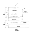
- Figure 1 depicts a cross sectional view of a light emitting device 100 that may incorporate various optional layers that rely on polarization enhanced doping achieved by a varying Al composition.
- the light emitting device 100 includes an active region 105 disposed between a p-side heterostructure 120 and an n-side heterostructure 110.
- the p-side heterostructure 120 may comprises a p-side short period superlattice (SPSL) 121 comprising alternating layers of Al xhigh Ga 1-xhigh N/Al xlow Ga 1-xlow N, where x high can range from about 1 to about 0.5 and x low can range from about 0.75 to about 0, for example.
- SPSL p-side short period superlattice
- P-contact layer 122 is disposed between the SPSL 121 and the p-contact, which may be a metal such as palladium (Pd).
- the p-contact layer 122 may comprise Al z Ga 1-z N and may be graded according to an Al composition profile that decreases as a function of distance in a direction from the SPSL 121 towards the p-contact.
- the layers of the n-side heterostructure 110, active region 105, and p-side heterostructure 120 can be epitaxially grown on a substrate comprising a hexagonal symmetry material, such as a group III-nitride material.
- a substrate comprising a hexagonal symmetry material, such as a group III-nitride material.
- Suitable materials for the substrate may comprise one or more of GaN, AlN, SiC, sapphire, Si, GaAs, ZnO, a group III-N alloy, and a template comprising a group III-N material.
- the layers of the light emitting device 100 may be grown on a polar or semi-polar surface or facet of the substrate.
- the substrate may comprise sapphire, a group-III nitride, SiC, or ZnO, wherein the n-side heterostructure, active region and p-side heterostructure are epitaxially grown on an (0001) or (000 1 ) surface of the substrate.
- the substrate may comprise a group-III nitride, SiC, or ZnO, wherein the n-side heterostructure, active region and p-side heterostructure are epitaxially grown on a semi-polar facet of the substrate.
- the active region 105 may include one or more quantum wells that are separated by barriers and/or multiple quantum well structures that are separated by spacers. Electrons from the n-side of the device and holes from the p side of the device diffuse to the active region 105 where they can recombine to generate light.
- the quantum wells, barriers, and/or spacers may be formed using any nitride based material system, such as InGaN, AlGaN, InAlN, InAlGaN, or other nitrides, or polar oxides such as the BeMgZnO system.
- an electron blocking layer (EBL) 125 is disposed between the last quantum well structure of the active 105 region and the p side heterostructure 120 to help contain electrons within the active region 105. Because light emission depends on recombination of holes and electrons in the active region 105, it is beneficial to retain electrons in the active region to increase the likelihood of recombination.
- AlGaN used in the p-side layers 120 must be sufficiently conductive and at the same time sufficiently transparent at the lasing wavelength.
- Magnesium can be used as a p-type dopant for AlGaN, and because the energy of the Mg acceptor level in AlGaN increases with Al composition, it becomes more difficult to achieve high hole concentration and conductivity as the Al composition increases.
- Transparency is more readily achieved in AlGaN when Al composition is large, and this places a competing constraint on Al composition in the p-side layers.
- Another constraint is the need to establish a good electrical contact between the nitride material and the metal electrode of the p-contact. This requirement is more readily satisfied by forming the contact between a metal and GaN (approximately zero Al composition).
- Embodiments discussed herein involve designs for p-layer structures that simultaneously achieve sufficient p-type conductivity, sufficient optical transparency and enable the establishment of a low resistivity electrical contact between the p-type material and the metal electrode.
- the approaches discussed herein can involve an acceptor-doped Al xhigh Ga 1-xhigh N/Al xlow Ga 1-xlow N SPSL 121 that can optionally be used in conjunction with a acceptor-doped graded AlGaN p-contact layer 122 that connects the SPSL 121 to a metal p-contact.
- a suitable acceptor for AlGaN comprises magnesium (Mg).
- Other possible p-type dopants for AlGaN include Be and C.
- the graded p-contact layer may comprise Al z Ga 1-z N where z is graded according to a profile, which may be constant, linear, parabolic, and/or S-shaped, for example. Sufficiently low optical absorption losses, sufficiently high p-type conductivity, and a good electrical contact can be achieved with these approaches.
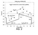
- Figure 2 illustrates polarization enhanced doping in an SPSL.
- the c-axis of the AlGaN is perpendicular to the plane of the layers.
- This discontinuity in the polarization gives rise to an electric field in each layer, which, together with the valence band offset between Al xhigh Ga 1-xhigh N layers, e.g., AlN in Figure 2 and the Al xlow Ga 1-xlow N layers, e.g., Al 0.5 Ga 0.5 N in Figure 2 , gives rise to a modulation of the potential within the crystal.
- the modulation of the potential leads to the ionization of p-type dopants and the formation of holes.
- P-type dopants (such as Mg atoms) that are located in layers with high Al composition are likely to become ionized by capturing an electron. The electron is removed from the layers with lower Al composition, and this creates a hole.
- the holes tend to accumulate at an interface between the layers as indicated schematically in Fig. 2 .
- Figure 2 shows calculated transition levels 210, 211 for Mg atoms.
- the dashed line represents the calculated Fermi energy 220 and the solid line represents the valence band maximum 220 of the SPSL.
- the transition level 211 for a given Mg atom is below the Fermi energy 220, that Mg atom will likely be ionized and in a negatively charged state.
- Mg atoms located in the Al-rich part of the SPSL have transition levels 211 that are below the valence band maximum 230 of the SPSL structure. These Mg atoms will likely become negatively charged and this gives rise to holes 240.
- the Mg atoms located in regions having less Al have transition levels 210 that are above the Fermi energy 220. These Mg atoms are likely to remain in the neutral charge state.
- the SPSL gives rise to a modulation in the valence band edge.
- the modulation of the valence band edge in a short period SPSL is approximately equal to the sum of the valence band offset (VBO) between the two materials in the SPSL and the change in potential in the SPSL arising from the polarization charges at the interfaces.
- VBO valence band offset
- P xlow and P xhigh are the polarizations in the Al xlow Ga 1-xlow N and the Al xhigh Ga 1-xhigh N and ⁇ xhigh and ⁇ xlow are the dielectric constants of the two materials.
- the change in potential across the SPSL segment of thickness T high is T high E xhigh and the change in potential across the superlattice segment of thickness T low is T low E xlow .
- T high E xhigh - T low E xlow .
- the total modulation of the valence band edge (V mod ) is the sum of the contributions arising from the band offset and the polarization fields.
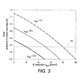
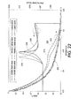
- V mod is plotted in Figure 3 as a function of x low for a fixed x high . For the simulation of Figure 3 , T high and T low are each equal to one nanometer.
- the SPSL has a total modulation in the valence band potential that is comparable (e.g., about equal) to the energy of the acceptor level of the p-type dopant.
- the most common acceptor is Mg and the energy of the acceptor level in Al 0.5 Ga 0.5 N is approximately 0.35 eV above the valence band maximum, as shown by the dashed line 310 in Figure 3 .
- the modulation of the valence band produced by the SPSL is sufficiently large, the number of ionized acceptors is significantly enhanced in comparison to a homogeneous layer. This requirement places a constraint on the Al compositions in the SPSL.
- x high and x low should be greater than about 0.25 in order to achieve a significant benefit from the polarization enhanced approach.
- the device illustrated in Figure 1 can be grown in a polar orientation on the group-III face (0001) of the III-N material, e.g., the Al face of an AlN substrate. It is also possible to exploit polarization enhanced doping in devices grown on a semi-polar facet of the substrate. For semi-polar orientations, however, the change in polarization at the interfaces is reduced, and so the electric fields in the layers are reduced in comparison to c-plane interfaces. Thus, the enhancement of hole concentration is expected to be reduced in devices grown in semi-polar orientations as compared with devices grown in polar orientations.
- An SPSL comprising 1 nm layers of AlN/ Al 0.5 Ga 0.5 N illustrates one configuration, note that other layer thicknesses and compositions can also be useful.
- a larger contrast in Al composition may be useful.
- a lattice that includes alternating layers of Al 0.25 Ga 0.75 N and AlN (75% contrast) would provide additional contrast when compared to the Al 0.5 Ga 0.5 N/AlN embodiment.
- the amount of contrast may be constrained by a maximum Al composition and a minimum Al composition. For example, it becomes more difficult to incorporate the p-type dopant into a layer that has a very high Al content, e.g., above 0.9.
- optimal Al compositions for the layers of the polarization enhanced SPSL may alternate from x high less than about 0.9 to x low greater than about 0.44.
- the thicknesses of the AlGaN layers in the polarization enhanced SPSL must be sufficiently small so that vertical transport of holes perpendicular to the layers is possible.
- the band gap of bulk Al x Ga 1-x N for x less than about 0.5 is too low to prevent absorption of light at wavelengths less than or equal to 250 nm.
- quantum confinement in the SPSL increases the energy gap of the SPSL so that absorption of light in an SPSL having alternating layers AlN/Al 0.5 Ga 0.5 N/or Al xhigh Ga 1-xhigh N/Al xlow Ga 1-xlow N with average Al composition of greater than about 0.60, e.g., Al 0.74 Ga 0.26 N/Al 0.44 Ga 0.56 N, would be acceptably low.
- This type of SPSL is therefore appropriate for a laser emitting at around 250 nm.
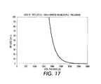
- Figure 5 is a graph that shows the optical transmission spectra of a p-side SPSL hole transport layer comprising 1.02 nm layers of Al 0.5 Ga 0.5 N alternating with 1.45 nm layers of AlN (shown in graph 510) and a similar superlattice with thicker AlGaN/AlN layers (6.15 nm layers of Al 0.5 Ga 0.5 N alternating with 6 nm layers of AlN) (shown in graph 520).
- the thicknesses, T high , and T low , of individual layers of an Al xhigh /Ga 1-xhigh N/Al xlow Ga 1-xlow /N within the SPSL may be only a few (e.g., 6) atomic bi-layers thick, as previously discussed.
- the high polarization fields within the SPSL promotes ionization of dopants, leading to improved hole generation and to lower electrical conductivity.
- Figure 6 shows the calculated band structure of an Mg doped Al 0.74 Ga 0.26 N/Al 0.49 Ga 0.51 N SPSL, where T high is 0.7 nm and T low is 0.9 nm.
- FIG. 7 is a cross section transmission electron micrograph (TEM) showing the SPSL structures that maintain sharp interfaces between the thin layers having thicknesses T high and T low of less about 1 nm.
- the AlGaN/AlGaN SPSL shown in Figure 7 was grown using metal organic chemical vapor deposition (MOCVD).
- MOCVD metal organic chemical vapor deposition
- Processes disclosed herein include heterostructure crystal growth conditions that enable sharp interfaces to be formed between such ultra-thin layers. It can be challenging to grow these SPSLs that vary the Al composition across thin layers with sharp interfaces because if appropriate growth conditions are not maintained, the very thin layers can merge into one alloy. For example, in some cases, growing the SPSL layers at temperatures of about 930 to 980°C and pressure of about 200 torr allows for optimal crystal quality and incorporation of Mg dopants.
- layers are grown at a rate of 0.01 to 0.04 nm per sec, corresponding to a metal organic Trimethylgallium (TMG) flow rate of 0.5 sccm and to an ammonia flow rate of 4 liters per minute.
- TMG metal organic Trimethylgallium
- the high ammonia flow rate relative to TMG leads to a high V-III partial pressure, which can provide high crystal quality.
- the layers can be grown under relatively low ambient pressures of between about 80 torr up to about 700 torr and at a relatively low temperature between about 750°C and about 1300°C.
- the selected growth temperature needs to achieve acceptable crystal quality, acceptor donor incorporation, and relatively sharp features between the layers of the SPSL.
- Figure 8 shows the test geometry used for temperature testing of the SPSLs. Test devices were fabricated by forming Pd p-contacts on the p-contact layer (p+ GaN layer) and etching away the p+GaN layer material at regions between the contacts. The pattern of the p-contacts is processed into Van Der Pauw pattern for resistivity measurement.
- the corresponding average aluminum composition is 60% for both SPSLs is, and they both behave optically like 60% AlGaN.
- One structure was grown at a temperature of 940 °C, while the other structure was grown at 980 °C.
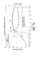
- Figure 9 shows that the lateral electrical resistivities of these test SPSLs have nearly a-thermal behaviors, wherein the lateral resistivity changes by less than about 50 ⁇ -cm over a temperature range of 400 K to 100 K.
- the sample grown at 940 °C and the sample grown at 980 °C show similar behaviors. This weak temperature dependence suggests that the doping ionization mechanism is indeed a-thermal, which would be expected in the polarization-induced hole activation process previously described
- Figure 9 also plots the resistivity behavior of p-doped GaN and homogeneous p-doped Al 0.7 Ga 0.3 N.
- Both the p-GaN and the homogeneous p-AlGaN exhibit sharp increases in electrical resistivities with reduced temperatures as is characteristic of thermal hole activation.
- the thermal activation energy of the SPSL samples are 22 meV and 17 meV for the 940 °C and the 980 °C samples, respectively.
- the activation energies are 323 meV for the homogeneous p-AlGaN and 146 meV for the p-GaN.
- the AlGaN polarization enhanced SPSL designs described herein produce low resistivity of about 20 ⁇ -cm at temperatures less than about 175 K and/or about 10 ⁇ -cm at room temperature.
- FIG 10 shows a three dimensional schematic view of the test structure used for IV testing of the SPSL structures.
- the test structure 1000 is a light emitting device that includes an AlN substrate 1010 with n-side heterostructure 1020, active region 1040, and p-side heterostructure 1035 (that includes the polarization enhanced SPSL) grown in that order on the AlN substrate 1010.
- a metallic n-contact 1030 makes electrical contact to the n-side heterostructure and a metallic p-contact 1050 makes electrical contact with the p-side heterostructure.
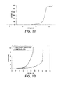
- Figure 11 shows the DC current-voltage (IV) characteristics of devices utilizing the polarization enhanced SPSL.
- a graded p-contact layer 122 may be used alone or in conjunction with the polarization enhanced SPSLs described above.
- the graded p-contact layer has higher Al composition at the interface between the p-heterostructure and the p-contact layer and a lower Al composition at the interface between the p-contact layer and the p-contact.
- the Al composition decreases linearly or piece-wise linearly across the p-contact layer, although other profiles are also useful, as discussed herein.
- FIG. 13 A simulation of the band structure for a device containing both a polarization enhanced SPSL and a graded Al z Ga 1-z N p-contact layer is shown in Figure 13 .
- the Al composition in the p-contact region produces a three-dimensional hole gas that extends over a region of thickness D , where D can be the thickness of the p-contact (if the grading is done across the entire layer, or other thickness across which the grading occurs.
- D can be the thickness of the p-contact (if the grading is done across the entire layer, or other thickness across which the grading occurs.
- Figure 15 shows polarization fields in Coulombs per meter squared (C/m 2 ) for a linearly graded Al z Ga 1-z N p-contact layer with respect to distance.
- Figure 16 shows the hole concentration in the Al z Ga 1-z N p-contact layer with respect to distance for the linearly graded design.
- the thickness of the p-contact layer, D is 100 nm and z changes from 0.7 to 0.
- the total polarization 1510 is dependent on the spontaneous polarization 1520 and piezoelectric polarization 1530, which arises from strain in the layer.
- the hole concentration is substantially uniform across the 100 nm layer.
- the polarization field of the graded layer creates a nearly uniform hole gas and therefore enhances conductivity in the vertical direction (the [0001] direction) through the device.
- the thickness and the effective index of refraction of the SPSL should be sufficient to prevent the lasing mode from overlapping with absorbing regions, such as the graded layer and metal contacting electrode.
- total thickness of such an SPSL should be greater than about 250 nm (2500 ⁇ ) to reduce the combined absorption loss in the graded p-contact layer and the Pd metal contact to below 10 cm -1 . This absorption loss should be sufficient to obtain lasing.
- Figure 18 illustrates three examples of hole concentrations calculated for several non-linear graded Al composition profiles. Graphs depicting three exemplary non-linear profiles are provided at the right side of Figure 18 . At the left side of Figure 18 , hole concentrations produced by the non-linear configurations are shown. Figure 18 depicts three example profiles and corresponding hole concentrations denoted as top, middle, and bottom examples. In each example, the Al composition decreases from 0.7 to zero over a 100 nm distance.
- An appropriate grading profile sustains a high hole concentration, (10 18 -10 19 cm -3 ) across substantially all of the p-contact layer.
- the slightly non-linear profile shown in the top example of Figure 18 provides a substantially uniform and high concentration across the profile distance.
- the Al composition profile changes over a substantial majority of the profile distance.
- the profile shown in the middle example is more non-linear when compared to the top profile, and has slightly higher hole concentration at side of the layer that would be proximate the p-contact when compared to the top example.
- a "step profile,” as shown in the bottom example of Figure 18 leads to an accumulation of holes at the interfaces and reduced hole concentrations in regions between the interfaces. The regions of lower hole concentration are more resistive ( ⁇ 10 17 cm -3 ) and therefore in many cases the top and middle profiles would be more desirable.
- Linear graded, parabolic graded, and graded "S" profiles may be considered for the p-contact layer.
- the Al composition in the p-contact layer is higher at or near the interface between the p-side heterostructure and the p-contact layer and when compared to the Al composition at or near the interface between the p-contact layer and the p-contact.
- the graded profiles in the p-contact layer include an Al composition changes over a substantial majority of the distance between the p-side heterostructure and the p-contact.
- Both "parabolic" and “S” designs utilize built-in piezoelectric and spontaneous polarization and can induce over 1 x 10 18 /cm 3 hole concentration across the layers in simulation.
- the S design can effectively suppress the absorption loss from the contact and the layer itself to 14 cm -1 , which is about one third of linear (40 cm -1 ) and/or parabolic (44 cm -1 ) designs.
- An appropriate design rule for an S-graded layer includes that the Al composition of AlGaN that gives the highest refractive index at the lasing wavelength should occur at the waist of S.
- the "waist" of the S profile, d w is an inflection point where the curve corresponding to Al composition vs. distance has a change in curvature from positive to negative.
- the extinction coefficient, k relates to the absorption of light in the layer.
- the average composition of the SPSL requires z to be higher than 0.62 in order to provide optical mode confinement (low refractive index) and high transparency (low k).
- This local energy trap attracts the optical mode and therefore enhances the overlaps with absorbing portion (higher k). In other words, the mode tends to be "attracted” to regions where the material exhibits a relatively higher index of refraction. If the mode extends more into regions with higher loss, then the total loss will be greater.
- the total thickness of the p-contact layer, D may be about 100 nm, for example.
- the tables shown in Figure 21 provide values of z at various values of d for each of the profiles.
- Traces 2210, 2220, 2230 show the refractive index of the linear, parabolic, and S profiles, respectively, with respect to distance.
- Traces 2215, 2225, 2235 show the optical mode for the linear, parabolic, and S profiles, respectively, with respect to distance.
- the relatively broad peak in the index induces a hump 2216 in the optical mode plot 2215.
- the hump 2216 in the optical mode 2215 of the linear profile may increase the optical loss since it causes an increased extension of the optical mode into lossy material where z ⁇ 0.62.
- the loss incurred in the linear design is 40 cm -1 .
- the optical mode trace 2225 for the parabolic graded profile pushes the point for which the peak index occurs to a larger distance from the interface between the p-contact layer and the SPSL.
- the width of the index peak is increased by the parabolic design, and as a result, the optical loss incurred in the parabolic design (44 cm -1 ) is greater than in the linear graded design.
- the peak is narrowed, as shown in trace 2230. The distance from interface to the index peak is extended in the S design and this helps to suppress the loss.
- the absorption loss in the S-shaped design is reduced to about 14 cm -1 . This absorption loss is about one third of 40 cm -1 and 44 cm -1 of linear and parabolic designs, respectively.
- An appropriately designed graded p-contact layer in a light emitting device can enable the use of an SPSL having a reduced thickness when compared with a light emitting device employing a p-contact layer having a substantially constant Al composition.
- a magnitude of g 2 is greater than a magnitude of g 1 .
- a thickness of the SPSL may be less than about 260 nm for d mid greater than about 60 nm.
- the thickness of the SPSL may be less than about 260 nm for d W greater than about 60 nm.
- the SPSL layers may extend to the active region.
- Figure 25 is an energy diagram that shows the conduction band energy in the region of the quantum wells 2512, in the region of the last barrier 2520 of the active region and in the region of the polarization enhanced SPSL 2530.
- the polarization enhanced SPSL 2530 is immediately adjacent to the last barrier 2520 which in turn is immediately adjacent the last quantum well 2511 of the active region.
- the dimensions and/or composition of the SPSL may be modified near the active region forming a section of the SPSL that provides the functionality of an electron blocking layer (EBL) for the active region.
- EBL electron blocking layer
- An example of this approach is illustrated by the conduction band energy diagram of Figure 26 .
- several of the SPSL layers e.g., about six SPSL layers near the active region 2610, form a multilayer electron blocking section (MEBS) 2640.
- the SPSL layers of the MEBS 2640 have modified thickness and/or composition (T high , T low , x high , x low ) when compared to the standard layers of the SPSL 2630.
- x high and x low of the standard SPSL layers are 0.74 and 0.44, respectively; T high and T low of the standard SPSL layers are both 1.0 nm and 1.0 nm.
- Other values of x high , x low , T high , T low are possible so long as the Al compositions and/or layer thicknesses of the MEBS layers are selected to provide significant retention of electrons in the active region.
- Systems, devices or methods disclosed herein may include one or more of the features, structures, methods, or combinations thereof described herein.
- a device or method may be implemented to include one or more of the features and/or processes described herein. It is intended that such device or method need not include all of the features and/or processes described herein, but may be implemented to include selected features and/or processes that provide useful structures and/or functionality.
- numeric values and ranges are provided for various aspects of the implementations described. These values and ranges are to be treated as examples only, and are not intended to limit the scope of the claims. For example, embodiments described in this disclosure can be practiced throughout the disclosed numerical ranges. In addition, a number of materials are identified as suitable for various implementations. These materials are to be treated as exemplary, and are not intended to limit the scope of the claims.
Landscapes
- Physics & Mathematics (AREA)
- Optics & Photonics (AREA)
- Condensed Matter Physics & Semiconductors (AREA)
- General Physics & Mathematics (AREA)
- Electromagnetism (AREA)
- Engineering & Computer Science (AREA)
- Chemical & Material Sciences (AREA)
- Nanotechnology (AREA)
- Geometry (AREA)
- Life Sciences & Earth Sciences (AREA)
- Biophysics (AREA)
- Crystallography & Structural Chemistry (AREA)
- Led Devices (AREA)
- Semiconductor Lasers (AREA)
- Materials Engineering (AREA)
Applications Claiming Priority (1)
| Application Number | Priority Date | Filing Date | Title |
|---|---|---|---|
| US13/619,598 US9401452B2 (en) | 2012-09-14 | 2012-09-14 | P-side layers for short wavelength light emitters |
Publications (3)
| Publication Number | Publication Date |
|---|---|
| EP2709170A2 true EP2709170A2 (de) | 2014-03-19 |
| EP2709170A3 EP2709170A3 (de) | 2015-03-04 |
| EP2709170B1 EP2709170B1 (de) | 2017-07-26 |
Family
ID=49165603
Family Applications (1)
| Application Number | Title | Priority Date | Filing Date |
|---|---|---|---|
| EP13184374.0A Not-in-force EP2709170B1 (de) | 2012-09-14 | 2013-09-13 | P-Seitenschichten für Kurzwellen-Lichtemitter |
Country Status (4)
| Country | Link |
|---|---|
| US (2) | US9401452B2 (de) |
| EP (1) | EP2709170B1 (de) |
| JP (1) | JP6259611B2 (de) |
| KR (1) | KR101941296B1 (de) |
Cited By (8)
| Publication number | Priority date | Publication date | Assignee | Title |
|---|---|---|---|---|
| CN104134730A (zh) * | 2014-08-19 | 2014-11-05 | 湘能华磊光电股份有限公司 | Mg掺杂电子阻挡层的外延片,生长方法及LED结构 |
| JP2017517148A (ja) * | 2014-05-27 | 2017-06-22 | ザ・シランナ・グループ・プロプライエタリー・リミテッドThe Silanna Group Pty Limited | 半導体構造と超格子とを用いた高度電子デバイス |
| EP3486939A1 (de) * | 2017-11-20 | 2019-05-22 | IMEC vzw | Verfahren zur formung einer halbleiterstruktur für eine galliumnitridkanalvorrichtung |
| US10475956B2 (en) | 2014-05-27 | 2019-11-12 | Silanna UV Technologies Pte Ltd | Optoelectronic device |
| US10475954B2 (en) | 2014-05-27 | 2019-11-12 | Silanna UV Technologies Pte Ltd | Electronic devices comprising n-type and p-type superlattices |
| US11322643B2 (en) | 2014-05-27 | 2022-05-03 | Silanna UV Technologies Pte Ltd | Optoelectronic device |
| EP3869571A4 (de) * | 2018-10-17 | 2022-07-20 | Stanley Electric Co., Ltd. | Lichtemittierendes halbleiterelement |
| WO2026083205A1 (en) * | 2024-10-15 | 2026-04-23 | Silanna UV Technologies Pte Ltd | Polar semiconductor superlattice with energy barrier |
Families Citing this family (36)
| Publication number | Priority date | Publication date | Assignee | Title |
|---|---|---|---|---|
| GB201211038D0 (en) | 2012-06-21 | 2012-08-01 | Norwegian Univ Sci & Tech Ntnu | Solar cells |
| US9401452B2 (en) | 2012-09-14 | 2016-07-26 | Palo Alto Research Center Incorporated | P-side layers for short wavelength light emitters |
| US9960315B2 (en) * | 2013-01-09 | 2018-05-01 | Sensor Electronic Technology, Inc. | Light emitting heterostructure with partially relaxed semiconductor layer |
| US9312428B2 (en) * | 2013-01-09 | 2016-04-12 | Sensor Electronic Technology, Inc. | Light emitting heterostructure with partially relaxed semiconductor layer |
| US20160005919A1 (en) * | 2013-02-05 | 2016-01-07 | Tokuyama Corporation | Nitride semiconductor light emitting device |
| US9412911B2 (en) | 2013-07-09 | 2016-08-09 | The Silanna Group Pty Ltd | Optical tuning of light emitting semiconductor junctions |
| KR101804493B1 (ko) * | 2013-09-03 | 2017-12-04 | 센서 일렉트로닉 테크놀로지, 인크 | 변조 도핑을 갖는 광전자 디바이스 |
| US10903391B2 (en) * | 2013-09-03 | 2021-01-26 | Sensor Electronic Technology, Inc. | Optoelectronic device with modulation doping |
| US9647168B2 (en) * | 2013-09-03 | 2017-05-09 | Sensor Electronic Technology, Inc. | Optoelectronic device with modulation doping |
| US10804423B2 (en) | 2013-09-03 | 2020-10-13 | Sensor Electronic Technology, Inc. | Optoelectronic device with modulation doping |
| US9444224B2 (en) * | 2014-12-08 | 2016-09-13 | Palo Alto Research Center Incorporated | Nitride laser diode with engineered non-uniform alloy composition in the n-cladding layer |
| US10347791B2 (en) | 2015-07-13 | 2019-07-09 | Crayonano As | Nanowires or nanopyramids grown on graphitic substrate |
| CN108292694A (zh) | 2015-07-13 | 2018-07-17 | 科莱约纳诺公司 | 纳米线/纳米锥形状的发光二极管及光检测器 |
| EA201890238A1 (ru) | 2015-07-31 | 2018-08-31 | Крайонано Ас | Способ выращивания нанопроволок или нанопирамидок на графитовых подложках |
| JP6573076B2 (ja) * | 2016-02-01 | 2019-09-11 | パナソニック株式会社 | 紫外線発光素子 |
| WO2017145026A1 (en) | 2016-02-23 | 2017-08-31 | Silanna UV Technologies Pte Ltd | Resonant optical cavity light emitting device |
| US10418517B2 (en) | 2016-02-23 | 2019-09-17 | Silanna UV Technologies Pte Ltd | Resonant optical cavity light emitting device |
| US10340415B2 (en) * | 2016-09-01 | 2019-07-02 | Lg Innotek Co., Ltd. | Semiconductor device and semiconductor device package including the same |
| WO2018048275A1 (ko) | 2016-09-10 | 2018-03-15 | 엘지이노텍 주식회사 | 반도체 소자 |
| EP3514840A4 (de) | 2016-09-13 | 2019-08-21 | LG Innotek Co., Ltd. | Halbleiterbauelement und halbleiterbauelementgehäuse damit |
| US10903395B2 (en) | 2016-11-24 | 2021-01-26 | Lg Innotek Co., Ltd. | Semiconductor device having varying concentrations of aluminum |
| US10121932B1 (en) * | 2016-11-30 | 2018-11-06 | The United States Of America As Represented By The Secretary Of The Navy | Tunable graphene light-emitting device |
| KR102688666B1 (ko) * | 2017-01-20 | 2024-07-25 | 쑤저우 레킨 세미컨덕터 컴퍼니 리미티드 | 반도체 소자 및 이를 포함하는 반도체 소자 패키지 |
| GB201705755D0 (en) | 2017-04-10 | 2017-05-24 | Norwegian Univ Of Science And Tech (Ntnu) | Nanostructure |
| CN107180898B (zh) * | 2017-05-09 | 2019-05-17 | 天津三安光电有限公司 | 发光二极管 |
| KR102390828B1 (ko) | 2017-08-14 | 2022-04-26 | 쑤저우 레킨 세미컨덕터 컴퍼니 리미티드 | 반도체 소자 |
| JP7228176B2 (ja) * | 2017-11-10 | 2023-02-24 | 豊田合成株式会社 | Iii族窒化物半導体発光素子 |
| WO2020012392A1 (en) * | 2018-07-13 | 2020-01-16 | Silanna UV Technologies Pte Ltd | Semiconductor-metal contacts with spontaneous and induced piezoelectric polarization |
| US10622514B1 (en) | 2018-10-15 | 2020-04-14 | Silanna UV Technologies Pte Ltd | Resonant optical cavity light emitting device |
| JP6793863B2 (ja) * | 2019-01-22 | 2020-12-02 | Dowaエレクトロニクス株式会社 | 深紫外発光素子用の反射電極の製造方法、深紫外発光素子の製造方法および深紫外発光素子 |
| JP7338166B2 (ja) * | 2019-02-25 | 2023-09-05 | 日本電信電話株式会社 | 半導体装置 |
| US10950750B2 (en) * | 2019-03-06 | 2021-03-16 | Bolb Inc. | Heterostructure and light-emitting device employing the same |
| GB201913701D0 (en) | 2019-09-23 | 2019-11-06 | Crayonano As | Composition of matter |
| US11342484B2 (en) | 2020-05-11 | 2022-05-24 | Silanna UV Technologies Pte Ltd | Metal oxide semiconductor-based light emitting device |
| JP7512121B2 (ja) * | 2020-08-05 | 2024-07-08 | パナソニックホールディングス株式会社 | 半導体レーザ素子 |
| CN116581210B (zh) * | 2023-07-10 | 2023-09-19 | 江西兆驰半导体有限公司 | 发光二极管外延片及其制备方法、发光二极管 |
Family Cites Families (30)
| Publication number | Priority date | Publication date | Assignee | Title |
|---|---|---|---|---|
| JP3374737B2 (ja) * | 1997-01-09 | 2003-02-10 | 日亜化学工業株式会社 | 窒化物半導体素子 |
| US6128535A (en) | 1997-12-05 | 2000-10-03 | Cardiac Pacemakers, Inc. | Automatic capture verification in multisite cardiac pacing |
| CA2322490C (en) * | 1998-03-12 | 2010-10-26 | Nichia Chemical Industries, Ltd. | Nitride semiconductor device |
| JP3551101B2 (ja) * | 1999-03-29 | 2004-08-04 | 日亜化学工業株式会社 | 窒化物半導体素子 |
| JP3539896B2 (ja) * | 1999-06-10 | 2004-07-07 | 日本電信電話株式会社 | 半導体超格子を有する半導体装置 |
| US6515313B1 (en) | 1999-12-02 | 2003-02-04 | Cree Lighting Company | High efficiency light emitters with reduced polarization-induced charges |
| US6535536B2 (en) * | 2000-04-10 | 2003-03-18 | Fuji Photo Film Co., Ltd. | Semiconductor laser element |
| JP3631157B2 (ja) * | 2001-03-21 | 2005-03-23 | 日本電信電話株式会社 | 紫外発光ダイオード |
| JP2004281553A (ja) * | 2003-03-13 | 2004-10-07 | Nippon Telegr & Teleph Corp <Ntt> | 発光ダイオード |
| KR100718129B1 (ko) * | 2005-06-03 | 2007-05-14 | 삼성전자주식회사 | Ⅲ-Ⅴ족 GaN계 화합물 반도체 소자 |
| JP4705412B2 (ja) * | 2005-06-06 | 2011-06-22 | パナソニック株式会社 | 電界効果トランジスタ及びその製造方法 |
| KR100665364B1 (ko) * | 2005-12-28 | 2007-01-09 | 삼성전기주식회사 | 질화물 반도체 발광 소자 |
| US7619238B2 (en) | 2006-02-04 | 2009-11-17 | Sensor Electronic Technology, Inc. | Heterostructure including light generating structure contained in potential well |
| EP1883141B1 (de) * | 2006-07-27 | 2017-05-24 | OSRAM Opto Semiconductors GmbH | LD oder LED mit Übergitter-Mantelschicht |
| US20080054248A1 (en) * | 2006-09-06 | 2008-03-06 | Chua Christopher L | Variable period variable composition supperlattice and devices including same |
| US20090309127A1 (en) * | 2008-06-13 | 2009-12-17 | Soraa, Inc. | Selective area epitaxy growth method and structure |
| US7856040B2 (en) * | 2008-09-24 | 2010-12-21 | Palo Alto Research Center Incorporated | Semiconductor light emitting devices with non-epitaxial upper cladding |
| JP2010251712A (ja) * | 2009-03-26 | 2010-11-04 | Sony Corp | バイ・セクション型半導体レーザ素子及びその製造方法、並びに、バイ・セクション型半導体レーザ素子の駆動方法 |
| CN102474077B (zh) * | 2009-07-31 | 2014-08-06 | 日亚化学工业株式会社 | 氮化物半导体激光二极管 |
| JP2013502731A (ja) | 2009-08-21 | 2013-01-24 | ザ リージェンツ オブ ザ ユニバーシティ オブ カリフォルニア | ミスフィット転位を有する部分的または完全に弛緩したAlInGaN層による半極性窒化物量子井戸の異方性ひずみ制御 |
| US9368580B2 (en) * | 2009-12-04 | 2016-06-14 | Sensor Electronic Technology, Inc. | Semiconductor material doping |
| US8604461B2 (en) * | 2009-12-16 | 2013-12-10 | Cree, Inc. | Semiconductor device structures with modulated doping and related methods |
| JP2011187580A (ja) * | 2010-03-05 | 2011-09-22 | Sony Corp | 自励発振型半導体レーザ素子及びその駆動方法 |
| US8633468B2 (en) * | 2011-02-11 | 2014-01-21 | Sensor Electronic Technology, Inc. | Light emitting device with dislocation bending structure |
| US10134948B2 (en) | 2011-02-25 | 2018-11-20 | Sensor Electronic Technology, Inc. | Light emitting diode with polarization control |
| JP5737111B2 (ja) * | 2011-03-30 | 2015-06-17 | 豊田合成株式会社 | Iii族窒化物半導体発光素子 |
| US8748919B2 (en) * | 2011-04-28 | 2014-06-10 | Palo Alto Research Center Incorporated | Ultraviolet light emitting device incorporating optically absorbing layers |
| WO2013018937A1 (ko) * | 2011-07-29 | 2013-02-07 | 삼성전자주식회사 | 반도체 발광소자 |
| US9401452B2 (en) | 2012-09-14 | 2016-07-26 | Palo Alto Research Center Incorporated | P-side layers for short wavelength light emitters |
| US9219189B2 (en) | 2012-09-14 | 2015-12-22 | Palo Alto Research Center Incorporated | Graded electron blocking layer |
-
2012
- 2012-09-14 US US13/619,598 patent/US9401452B2/en active Active
-
2013
- 2013-08-21 JP JP2013171187A patent/JP6259611B2/ja not_active Expired - Fee Related
- 2013-08-28 KR KR1020130102297A patent/KR101941296B1/ko not_active Expired - Fee Related
- 2013-09-13 EP EP13184374.0A patent/EP2709170B1/de not_active Not-in-force
-
2016
- 2016-07-13 US US15/209,715 patent/US10164146B2/en active Active
Non-Patent Citations (1)
| Title |
|---|
| None |
Cited By (17)
| Publication number | Priority date | Publication date | Assignee | Title |
|---|---|---|---|---|
| US11563144B2 (en) | 2014-05-27 | 2023-01-24 | Silanna UV Technologies Pte Ltd | Advanced electronic device structures using semiconductor structures and superlattices |
| US11114585B2 (en) | 2014-05-27 | 2021-09-07 | Silanna UV Technologies Pte Ltd | Advanced electronic device structures using semiconductor structures and superlattices |
| JP2017517148A (ja) * | 2014-05-27 | 2017-06-22 | ザ・シランナ・グループ・プロプライエタリー・リミテッドThe Silanna Group Pty Limited | 半導体構造と超格子とを用いた高度電子デバイス |
| US12272764B2 (en) | 2014-05-27 | 2025-04-08 | Silanna UV Technologies Pte Ltd | Advanced electronic device structures using semiconductor structures and superlattices |
| US10475956B2 (en) | 2014-05-27 | 2019-11-12 | Silanna UV Technologies Pte Ltd | Optoelectronic device |
| US10475954B2 (en) | 2014-05-27 | 2019-11-12 | Silanna UV Technologies Pte Ltd | Electronic devices comprising n-type and p-type superlattices |
| US10483432B2 (en) | 2014-05-27 | 2019-11-19 | Silanna UV Technologies Pte Ltd | Advanced electronic device structures using semiconductor structures and superlattices |
| JP2020074405A (ja) * | 2014-05-27 | 2020-05-14 | シランナ・ユー・ブイ・テクノロジーズ・プライベート・リミテッドSilanna Uv Technologies Pte Ltd | 半導体構造と超格子とを用いた高度電子デバイス |
| US11862750B2 (en) | 2014-05-27 | 2024-01-02 | Silanna UV Technologies Pte Ltd | Optoelectronic device |
| US11322643B2 (en) | 2014-05-27 | 2022-05-03 | Silanna UV Technologies Pte Ltd | Optoelectronic device |
| CN104134730A (zh) * | 2014-08-19 | 2014-11-05 | 湘能华磊光电股份有限公司 | Mg掺杂电子阻挡层的外延片,生长方法及LED结构 |
| CN104134730B (zh) * | 2014-08-19 | 2017-03-08 | 湘能华磊光电股份有限公司 | Mg掺杂电子阻挡层的外延片,生长方法及LED结构 |
| US10991577B2 (en) | 2017-11-20 | 2021-04-27 | Imec Vzw | Method for forming a semiconductor structure for a gallium nitride channel device |
| EP3486939A1 (de) * | 2017-11-20 | 2019-05-22 | IMEC vzw | Verfahren zur formung einer halbleiterstruktur für eine galliumnitridkanalvorrichtung |
| EP3869571A4 (de) * | 2018-10-17 | 2022-07-20 | Stanley Electric Co., Ltd. | Lichtemittierendes halbleiterelement |
| US12027647B2 (en) | 2018-10-17 | 2024-07-02 | Stanley Electric Co., Ltd. | Semiconductor light-emitting element |
| WO2026083205A1 (en) * | 2024-10-15 | 2026-04-23 | Silanna UV Technologies Pte Ltd | Polar semiconductor superlattice with energy barrier |
Also Published As
| Publication number | Publication date |
|---|---|
| US20140231745A1 (en) | 2014-08-21 |
| US20160336481A1 (en) | 2016-11-17 |
| US10164146B2 (en) | 2018-12-25 |
| KR101941296B1 (ko) | 2019-01-22 |
| EP2709170A3 (de) | 2015-03-04 |
| US9401452B2 (en) | 2016-07-26 |
| JP2014116580A (ja) | 2014-06-26 |
| EP2709170B1 (de) | 2017-07-26 |
| KR20140035813A (ko) | 2014-03-24 |
| JP6259611B2 (ja) | 2018-01-10 |
Similar Documents
| Publication | Publication Date | Title |
|---|---|---|
| US10164146B2 (en) | P-side layers for short wavelength light emitters | |
| CN101689594B (zh) | 发射辐射的半导体本体 | |
| US10475956B2 (en) | Optoelectronic device | |
| US9219189B2 (en) | Graded electron blocking layer | |
| US8993996B2 (en) | Superlattice structure | |
| US20100187550A1 (en) | Light emitting diode | |
| US9412901B2 (en) | Superlattice structure | |
| US11862750B2 (en) | Optoelectronic device | |
| JP7709985B2 (ja) | Uv発光デバイス用埋め込みコンタクト層 | |
| US7417258B2 (en) | Semiconductor light-emitting device, and a method of manufacture of a semiconductor device | |
| Piprek et al. | Analysis of wavelength-dependent performance variations of GaN-based ultraviolet lasers | |
| CN106025018A (zh) | 超晶格结构 | |
| Paliwal et al. | GaN/InAlN chirped short period superlattice as strain free top cladding for blue laser diode | |
| WO2024197018A1 (en) | Thin quantum barrier with high aluminum content for ultraviolet light emitters | |
| US9768349B2 (en) | Superlattice structure | |
| EP3699964B1 (de) | Polarisierung elektrisches feld-assistiertes loch erzeugende und p-typ kontakt struktur, lichtemittierende vorrichtung und photodetektor damit | |
| Lee et al. | Optical properties and electronic subband structures in InxGa1− xN/GaN multiple quantum wells | |
| WO2013138573A1 (en) | Semiconductor material doping |
Legal Events
| Date | Code | Title | Description |
|---|---|---|---|
| PUAI | Public reference made under article 153(3) epc to a published international application that has entered the european phase |
Free format text: ORIGINAL CODE: 0009012 |
|
| AK | Designated contracting states |
Kind code of ref document: A2 Designated state(s): AL AT BE BG CH CY CZ DE DK EE ES FI FR GB GR HR HU IE IS IT LI LT LU LV MC MK MT NL NO PL PT RO RS SE SI SK SM TR |
|
| AX | Request for extension of the european patent |
Extension state: BA ME |
|
| PUAL | Search report despatched |
Free format text: ORIGINAL CODE: 0009013 |
|
| AK | Designated contracting states |
Kind code of ref document: A3 Designated state(s): AL AT BE BG CH CY CZ DE DK EE ES FI FR GB GR HR HU IE IS IT LI LT LU LV MC MK MT NL NO PL PT RO RS SE SI SK SM TR |
|
| AX | Request for extension of the european patent |
Extension state: BA ME |
|
| RIC1 | Information provided on ipc code assigned before grant |
Ipc: H01S 5/32 20060101ALI20150129BHEP Ipc: B82Y 20/00 20110101ALI20150129BHEP Ipc: H01L 33/00 20100101AFI20150129BHEP Ipc: H01L 33/32 20100101ALI20150129BHEP Ipc: H01S 5/343 20060101ALI20150129BHEP Ipc: H01L 21/02 20060101ALI20150129BHEP Ipc: H01L 33/06 20100101ALI20150129BHEP Ipc: H01L 33/14 20100101ALN20150129BHEP Ipc: H01S 5/042 20060101ALN20150129BHEP Ipc: H01S 5/20 20060101ALN20150129BHEP Ipc: H01S 5/30 20060101ALN20150129BHEP Ipc: H01S 5/34 20060101ALN20150129BHEP |
|
| 17P | Request for examination filed |
Effective date: 20150904 |
|
| RBV | Designated contracting states (corrected) |
Designated state(s): AL AT BE BG CH CY CZ DE DK EE ES FI FR GB GR HR HU IE IS IT LI LT LU LV MC MK MT NL NO PL PT RO RS SE SI SK SM TR |
|
| RIC1 | Information provided on ipc code assigned before grant |
Ipc: H01L 33/06 20100101ALI20161222BHEP Ipc: H01L 33/14 20100101ALN20161222BHEP Ipc: H01S 5/32 20060101ALI20161222BHEP Ipc: H01L 33/00 20100101AFI20161222BHEP Ipc: H01S 5/34 20060101ALN20161222BHEP Ipc: H01L 33/32 20100101ALI20161222BHEP Ipc: H01S 5/20 20060101ALN20161222BHEP Ipc: H01S 5/042 20060101ALN20161222BHEP Ipc: H01S 5/30 20060101ALN20161222BHEP Ipc: H01S 5/343 20060101ALI20161222BHEP Ipc: B82Y 20/00 20110101ALI20161222BHEP Ipc: H01L 21/02 20060101ALI20161222BHEP |
|
| RIC1 | Information provided on ipc code assigned before grant |
Ipc: H01S 5/20 20060101ALN20170105BHEP Ipc: H01L 33/06 20100101ALI20170105BHEP Ipc: B82Y 20/00 20110101ALI20170105BHEP Ipc: H01L 33/32 20100101ALI20170105BHEP Ipc: H01S 5/32 20060101ALI20170105BHEP Ipc: H01L 33/14 20100101ALN20170105BHEP Ipc: H01S 5/30 20060101ALN20170105BHEP Ipc: H01L 33/00 20100101AFI20170105BHEP Ipc: H01S 5/343 20060101ALI20170105BHEP Ipc: H01S 5/042 20060101ALN20170105BHEP Ipc: H01L 21/02 20060101ALI20170105BHEP Ipc: H01S 5/34 20060101ALN20170105BHEP |
|
| GRAP | Despatch of communication of intention to grant a patent |
Free format text: ORIGINAL CODE: EPIDOSNIGR1 |
|
| RIC1 | Information provided on ipc code assigned before grant |
Ipc: H01L 21/02 20060101ALI20170207BHEP Ipc: H01S 5/042 20060101ALN20170207BHEP Ipc: H01S 5/30 20060101ALN20170207BHEP Ipc: H01L 33/06 20100101ALI20170207BHEP Ipc: H01S 5/34 20060101ALN20170207BHEP Ipc: B82Y 20/00 20110101ALI20170207BHEP Ipc: H01S 5/20 20060101ALN20170207BHEP Ipc: H01L 33/32 20100101ALI20170207BHEP Ipc: H01S 5/32 20060101ALI20170207BHEP Ipc: H01L 33/14 20100101ALN20170207BHEP Ipc: H01L 33/00 20100101AFI20170207BHEP Ipc: H01S 5/343 20060101ALI20170207BHEP |
|
| INTG | Intention to grant announced |
Effective date: 20170221 |
|
| GRAS | Grant fee paid |
Free format text: ORIGINAL CODE: EPIDOSNIGR3 |
|
| GRAA | (expected) grant |
Free format text: ORIGINAL CODE: 0009210 |
|
| AK | Designated contracting states |
Kind code of ref document: B1 Designated state(s): AL AT BE BG CH CY CZ DE DK EE ES FI FR GB GR HR HU IE IS IT LI LT LU LV MC MK MT NL NO PL PT RO RS SE SI SK SM TR |
|
| REG | Reference to a national code |
Ref country code: GB Ref legal event code: FG4D |
|
| REG | Reference to a national code |
Ref country code: CH Ref legal event code: EP |
|
| REG | Reference to a national code |
Ref country code: AT Ref legal event code: REF Ref document number: 913052 Country of ref document: AT Kind code of ref document: T Effective date: 20170815 |
|
| REG | Reference to a national code |
Ref country code: FR Ref legal event code: PLFP Year of fee payment: 5 |
|
| REG | Reference to a national code |
Ref country code: IE Ref legal event code: FG4D |
|
| REG | Reference to a national code |
Ref country code: DE Ref legal event code: R096 Ref document number: 602013023961 Country of ref document: DE |
|
| REG | Reference to a national code |
Ref country code: NL Ref legal event code: MP Effective date: 20170726 |
|
| REG | Reference to a national code |
Ref country code: LT Ref legal event code: MG4D |
|
| REG | Reference to a national code |
Ref country code: AT Ref legal event code: MK05 Ref document number: 913052 Country of ref document: AT Kind code of ref document: T Effective date: 20170726 |
|
| PG25 | Lapsed in a contracting state [announced via postgrant information from national office to epo] |
Ref country code: FI Free format text: LAPSE BECAUSE OF FAILURE TO SUBMIT A TRANSLATION OF THE DESCRIPTION OR TO PAY THE FEE WITHIN THE PRESCRIBED TIME-LIMIT Effective date: 20170726 Ref country code: SE Free format text: LAPSE BECAUSE OF FAILURE TO SUBMIT A TRANSLATION OF THE DESCRIPTION OR TO PAY THE FEE WITHIN THE PRESCRIBED TIME-LIMIT Effective date: 20170726 Ref country code: HR Free format text: LAPSE BECAUSE OF FAILURE TO SUBMIT A TRANSLATION OF THE DESCRIPTION OR TO PAY THE FEE WITHIN THE PRESCRIBED TIME-LIMIT Effective date: 20170726 Ref country code: NO Free format text: LAPSE BECAUSE OF FAILURE TO SUBMIT A TRANSLATION OF THE DESCRIPTION OR TO PAY THE FEE WITHIN THE PRESCRIBED TIME-LIMIT Effective date: 20171026 Ref country code: NL Free format text: LAPSE BECAUSE OF FAILURE TO SUBMIT A TRANSLATION OF THE DESCRIPTION OR TO PAY THE FEE WITHIN THE PRESCRIBED TIME-LIMIT Effective date: 20170726 Ref country code: LT Free format text: LAPSE BECAUSE OF FAILURE TO SUBMIT A TRANSLATION OF THE DESCRIPTION OR TO PAY THE FEE WITHIN THE PRESCRIBED TIME-LIMIT Effective date: 20170726 Ref country code: AT Free format text: LAPSE BECAUSE OF FAILURE TO SUBMIT A TRANSLATION OF THE DESCRIPTION OR TO PAY THE FEE WITHIN THE PRESCRIBED TIME-LIMIT Effective date: 20170726 |
|
| PG25 | Lapsed in a contracting state [announced via postgrant information from national office to epo] |
Ref country code: IS Free format text: LAPSE BECAUSE OF FAILURE TO SUBMIT A TRANSLATION OF THE DESCRIPTION OR TO PAY THE FEE WITHIN THE PRESCRIBED TIME-LIMIT Effective date: 20171126 Ref country code: PL Free format text: LAPSE BECAUSE OF FAILURE TO SUBMIT A TRANSLATION OF THE DESCRIPTION OR TO PAY THE FEE WITHIN THE PRESCRIBED TIME-LIMIT Effective date: 20170726 Ref country code: LV Free format text: LAPSE BECAUSE OF FAILURE TO SUBMIT A TRANSLATION OF THE DESCRIPTION OR TO PAY THE FEE WITHIN THE PRESCRIBED TIME-LIMIT Effective date: 20170726 Ref country code: RS Free format text: LAPSE BECAUSE OF FAILURE TO SUBMIT A TRANSLATION OF THE DESCRIPTION OR TO PAY THE FEE WITHIN THE PRESCRIBED TIME-LIMIT Effective date: 20170726 Ref country code: ES Free format text: LAPSE BECAUSE OF FAILURE TO SUBMIT A TRANSLATION OF THE DESCRIPTION OR TO PAY THE FEE WITHIN THE PRESCRIBED TIME-LIMIT Effective date: 20170726 Ref country code: BG Free format text: LAPSE BECAUSE OF FAILURE TO SUBMIT A TRANSLATION OF THE DESCRIPTION OR TO PAY THE FEE WITHIN THE PRESCRIBED TIME-LIMIT Effective date: 20171026 Ref country code: GR Free format text: LAPSE BECAUSE OF FAILURE TO SUBMIT A TRANSLATION OF THE DESCRIPTION OR TO PAY THE FEE WITHIN THE PRESCRIBED TIME-LIMIT Effective date: 20171027 |
|
| PG25 | Lapsed in a contracting state [announced via postgrant information from national office to epo] |
Ref country code: DK Free format text: LAPSE BECAUSE OF FAILURE TO SUBMIT A TRANSLATION OF THE DESCRIPTION OR TO PAY THE FEE WITHIN THE PRESCRIBED TIME-LIMIT Effective date: 20170726 Ref country code: RO Free format text: LAPSE BECAUSE OF FAILURE TO SUBMIT A TRANSLATION OF THE DESCRIPTION OR TO PAY THE FEE WITHIN THE PRESCRIBED TIME-LIMIT Effective date: 20170726 Ref country code: CZ Free format text: LAPSE BECAUSE OF FAILURE TO SUBMIT A TRANSLATION OF THE DESCRIPTION OR TO PAY THE FEE WITHIN THE PRESCRIBED TIME-LIMIT Effective date: 20170726 |
|
| REG | Reference to a national code |
Ref country code: CH Ref legal event code: PL Ref country code: DE Ref legal event code: R097 Ref document number: 602013023961 Country of ref document: DE |
|
| PG25 | Lapsed in a contracting state [announced via postgrant information from national office to epo] |
Ref country code: SK Free format text: LAPSE BECAUSE OF FAILURE TO SUBMIT A TRANSLATION OF THE DESCRIPTION OR TO PAY THE FEE WITHIN THE PRESCRIBED TIME-LIMIT Effective date: 20170726 Ref country code: IT Free format text: LAPSE BECAUSE OF FAILURE TO SUBMIT A TRANSLATION OF THE DESCRIPTION OR TO PAY THE FEE WITHIN THE PRESCRIBED TIME-LIMIT Effective date: 20170726 Ref country code: MC Free format text: LAPSE BECAUSE OF FAILURE TO SUBMIT A TRANSLATION OF THE DESCRIPTION OR TO PAY THE FEE WITHIN THE PRESCRIBED TIME-LIMIT Effective date: 20170726 Ref country code: EE Free format text: LAPSE BECAUSE OF FAILURE TO SUBMIT A TRANSLATION OF THE DESCRIPTION OR TO PAY THE FEE WITHIN THE PRESCRIBED TIME-LIMIT Effective date: 20170726 Ref country code: SM Free format text: LAPSE BECAUSE OF FAILURE TO SUBMIT A TRANSLATION OF THE DESCRIPTION OR TO PAY THE FEE WITHIN THE PRESCRIBED TIME-LIMIT Effective date: 20170726 |
|
| PLBE | No opposition filed within time limit |
Free format text: ORIGINAL CODE: 0009261 |
|
| STAA | Information on the status of an ep patent application or granted ep patent |
Free format text: STATUS: NO OPPOSITION FILED WITHIN TIME LIMIT |
|
| REG | Reference to a national code |
Ref country code: IE Ref legal event code: MM4A |
|
| REG | Reference to a national code |
Ref country code: BE Ref legal event code: MM Effective date: 20170930 |
|
| PG25 | Lapsed in a contracting state [announced via postgrant information from national office to epo] |
Ref country code: LU Free format text: LAPSE BECAUSE OF NON-PAYMENT OF DUE FEES Effective date: 20170913 |
|
| 26N | No opposition filed |
Effective date: 20180430 |
|
| PG25 | Lapsed in a contracting state [announced via postgrant information from national office to epo] |
Ref country code: IE Free format text: LAPSE BECAUSE OF NON-PAYMENT OF DUE FEES Effective date: 20170913 Ref country code: CH Free format text: LAPSE BECAUSE OF NON-PAYMENT OF DUE FEES Effective date: 20170930 Ref country code: LI Free format text: LAPSE BECAUSE OF NON-PAYMENT OF DUE FEES Effective date: 20170930 |
|
| REG | Reference to a national code |
Ref country code: FR Ref legal event code: PLFP Year of fee payment: 6 |
|
| PG25 | Lapsed in a contracting state [announced via postgrant information from national office to epo] |
Ref country code: SI Free format text: LAPSE BECAUSE OF FAILURE TO SUBMIT A TRANSLATION OF THE DESCRIPTION OR TO PAY THE FEE WITHIN THE PRESCRIBED TIME-LIMIT Effective date: 20170726 Ref country code: BE Free format text: LAPSE BECAUSE OF NON-PAYMENT OF DUE FEES Effective date: 20170930 |
|
| PG25 | Lapsed in a contracting state [announced via postgrant information from national office to epo] |
Ref country code: MT Free format text: LAPSE BECAUSE OF NON-PAYMENT OF DUE FEES Effective date: 20170913 |
|
| PG25 | Lapsed in a contracting state [announced via postgrant information from national office to epo] |
Ref country code: HU Free format text: LAPSE BECAUSE OF FAILURE TO SUBMIT A TRANSLATION OF THE DESCRIPTION OR TO PAY THE FEE WITHIN THE PRESCRIBED TIME-LIMIT; INVALID AB INITIO Effective date: 20130913 |
|
| PG25 | Lapsed in a contracting state [announced via postgrant information from national office to epo] |
Ref country code: CY Free format text: LAPSE BECAUSE OF NON-PAYMENT OF DUE FEES Effective date: 20170726 |
|
| PG25 | Lapsed in a contracting state [announced via postgrant information from national office to epo] |
Ref country code: MK Free format text: LAPSE BECAUSE OF FAILURE TO SUBMIT A TRANSLATION OF THE DESCRIPTION OR TO PAY THE FEE WITHIN THE PRESCRIBED TIME-LIMIT Effective date: 20170726 |
|
| PG25 | Lapsed in a contracting state [announced via postgrant information from national office to epo] |
Ref country code: TR Free format text: LAPSE BECAUSE OF FAILURE TO SUBMIT A TRANSLATION OF THE DESCRIPTION OR TO PAY THE FEE WITHIN THE PRESCRIBED TIME-LIMIT Effective date: 20170726 |
|
| PG25 | Lapsed in a contracting state [announced via postgrant information from national office to epo] |
Ref country code: PT Free format text: LAPSE BECAUSE OF FAILURE TO SUBMIT A TRANSLATION OF THE DESCRIPTION OR TO PAY THE FEE WITHIN THE PRESCRIBED TIME-LIMIT Effective date: 20170726 |
|
| PG25 | Lapsed in a contracting state [announced via postgrant information from national office to epo] |
Ref country code: AL Free format text: LAPSE BECAUSE OF FAILURE TO SUBMIT A TRANSLATION OF THE DESCRIPTION OR TO PAY THE FEE WITHIN THE PRESCRIBED TIME-LIMIT Effective date: 20170726 |
|
| PGFP | Annual fee paid to national office [announced via postgrant information from national office to epo] |
Ref country code: GB Payment date: 20230823 Year of fee payment: 11 |
|
| PGFP | Annual fee paid to national office [announced via postgrant information from national office to epo] |
Ref country code: FR Payment date: 20230822 Year of fee payment: 11 Ref country code: DE Payment date: 20230822 Year of fee payment: 11 |
|
| REG | Reference to a national code |
Ref country code: DE Ref legal event code: R079 Ref document number: 602013023961 Country of ref document: DE Free format text: PREVIOUS MAIN CLASS: H01L0033000000 Ipc: H10H0020000000 |
|
| REG | Reference to a national code |
Ref country code: DE Ref legal event code: R119 Ref document number: 602013023961 Country of ref document: DE |
|
| GBPC | Gb: european patent ceased through non-payment of renewal fee |
Effective date: 20240913 |
|
| PG25 | Lapsed in a contracting state [announced via postgrant information from national office to epo] |
Ref country code: DE Free format text: LAPSE BECAUSE OF NON-PAYMENT OF DUE FEES Effective date: 20250401 |
|
| PG25 | Lapsed in a contracting state [announced via postgrant information from national office to epo] |
Ref country code: GB Free format text: LAPSE BECAUSE OF NON-PAYMENT OF DUE FEES Effective date: 20240913 |
|
| PG25 | Lapsed in a contracting state [announced via postgrant information from national office to epo] |
Ref country code: FR Free format text: LAPSE BECAUSE OF NON-PAYMENT OF DUE FEES Effective date: 20240930 |