EP2709209A1 - Dispositif de communication et système d'antenne à isolation élevée - Google Patents
Dispositif de communication et système d'antenne à isolation élevée Download PDFInfo
- Publication number
- EP2709209A1 EP2709209A1 EP13154045.2A EP13154045A EP2709209A1 EP 2709209 A1 EP2709209 A1 EP 2709209A1 EP 13154045 A EP13154045 A EP 13154045A EP 2709209 A1 EP2709209 A1 EP 2709209A1
- Authority
- EP
- European Patent Office
- Prior art keywords
- antenna
- communication device
- coupled
- feeding
- shorted
- Prior art date
- Legal status (The legal status is an assumption and is not a legal conclusion. Google has not performed a legal analysis and makes no representation as to the accuracy of the status listed.)
- Granted
Links
Images



Classifications
-
- H—ELECTRICITY
- H01—ELECTRIC ELEMENTS
- H01Q—ANTENNAS, i.e. RADIO AERIALS
- H01Q21/00—Antenna arrays or systems
- H01Q21/28—Combinations of substantially independent non-interacting antenna units or systems
-
- H—ELECTRICITY
- H01—ELECTRIC ELEMENTS
- H01Q—ANTENNAS, i.e. RADIO AERIALS
- H01Q1/00—Details of, or arrangements associated with, antennas
- H01Q1/52—Means for reducing coupling between antennas; Means for reducing coupling between an antenna and another structure
- H01Q1/521—Means for reducing coupling between antennas; Means for reducing coupling between an antenna and another structure reducing the coupling between adjacent antennas
- H01Q1/523—Means for reducing coupling between antennas; Means for reducing coupling between an antenna and another structure reducing the coupling between adjacent antennas between antennas of an array
-
- H—ELECTRICITY
- H01—ELECTRIC ELEMENTS
- H01Q—ANTENNAS, i.e. RADIO AERIALS
- H01Q1/00—Details of, or arrangements associated with, antennas
- H01Q1/12—Supports; Mounting means
- H01Q1/22—Supports; Mounting means by structural association with other equipment or articles
- H01Q1/24—Supports; Mounting means by structural association with other equipment or articles with receiving set
- H01Q1/241—Supports; Mounting means by structural association with other equipment or articles with receiving set used in mobile communications, e.g. GSM
- H01Q1/242—Supports; Mounting means by structural association with other equipment or articles with receiving set used in mobile communications, e.g. GSM specially adapted for hand-held use
- H01Q1/243—Supports; Mounting means by structural association with other equipment or articles with receiving set used in mobile communications, e.g. GSM specially adapted for hand-held use with built-in antennas
Definitions
- the disclosure generally relates to a communication device, and more particularly, relates to a communication device comprising an antenna system with high isolation.
- the smart phone has become one of the most indispensable mobile communication devices for modem people to use in their daily lives, allowing for convenience and timeliness.
- a user usually demands a variety of functions for smart phones.
- the smart phone is required to perform MIMO (Multi-Input Multi-Output) operations by multiple antennas therein to accelerate data transmission, or is required to have functions of dual-SIM, dual-standby, and dual-talk.
- MIMO Multi-Input Multi-Output
- a first SIM (Subscriber Identity Module) card of the smart phone is transmitting data through an antenna
- a second SIM card of the smart phone is capable of transmitting voice signals through another antenna; bringing convenience to a user with a dual-SIM smart phone.
- an antenna system with multiple antennas operating in a same band must be disposed in a small space of a mobile communication device (e.g., a smart phone). Since the antennas are very close to each other, mutual coupling and interference therebetween are enhanced, thereby degrading the performance of the antenna system. Thus, maintaining a high amount of isolation and reducing mutual coupling and interference between antennas are critical challenges for antenna designers.
- the invention is aimed to provide a communication device comprising an antenna system.
- the invention provides a resistive element, which is coupled between these antennas and attracts coupling currents on a feeding end of each antenna. Accordingly, the invention effectively improves the isolation between the antennas without negatively affecting the antenna efficiency.
- the disclosure is directed to a communication device, comprising: a ground element; and an antenna system, adjacent to the ground element, wherein the antenna system at least comprises: a first antenna; a second antenna, adjacent to the first antenna; a connection element, comprising a first portion and a second portion, wherein the first portion is coupled to the first antenna, and the second portion is coupled to the second antenna; and a resistive element, coupled between the first portion and the second portion of the connection element, wherein the connection element and the resistive element increase isolation between the first antenna and the second antenna.
- the disclosure is directed to a communication device, comprising: a ground element; and an antenna system, adjacent to the ground element, wherein the antenna system at least comprises: a first antenna, comprising a first feeding element; a second antenna, adjacent to the first antenna, and comprising a second feeding element; and a resistive element, coupled between the first feeding element and the second feeding element, wherein the resistive element increases isolation between the first antenna and the second antenna.
- the antenna system comprising at least the first antenna and the second antenna uses the connection element and the resistive element to increase the isolation between the first antenna and the second antenna.
- the poor isolation results from coupling currents being present between the antennas.
- the resistive element is disposed between the first antenna and the second antenna to absorb the coupling currents therebetween such that the isolation between the first antenna and the second antenna is enhanced. Accordingly, both the first antenna and the second antenna maintain good radiation efficiency.
- the resistive element is used to increase the isolation between the first antenna and the second antenna, wherein the resistive element is a chip resistor.
- the invention merely uses a simple chip resistor to effectively improve the resulting isolation of the antenna system.
- the resistance of the chip resistor is at least 75 ⁇ .
- the first antenna and the second antenna operate in at least one same mobile communication band. With the operation band of the first antenna overlapping with that of the second antenna, the isolation between the first antenna and the second antenna becomes meaningful.
- the first antenna further comprises a first feeding element
- the second antenna further comprises a second feeding element.
- the connection element is coupled between the first feeding element and the second feeding element. Accordingly, the resistive element can absorb the coupling currents between the first antenna and the second antenna via the connection element, and effectively improve the resulting isolation between the first antenna and the second antenna.
- the first antenna further comprises a first shorted element
- the second antenna further comprises a second shorted element.
- the connection element is coupled between the first shorted element and the second shorted element. Accordingly, the resistive element can absorb the coupling currents between the first antenna and the second antenna via the connection element, and effectively improve the isolation between the first antenna and the second antenna.
- the first antenna further comprises a first feeding element and a first shorted element
- the second antenna further comprises a second feeding element and a second shorted element.
- the connection element is coupled between the first feeding element and the second shorted element, or the connection element is coupled between the second feeding element and the first shorted element. Accordingly, the resistive element can absorb the coupling currents between the first antenna and the second antenna via the connection element, and effectively improve the resulting isolation between the first antenna and the second antenna.
- the antenna system is adjacent to a corner of the ground element, and the first antenna and the second antenna are adjacent to two edges of the ground element, respectively, wherein the edges of the ground element are substantially perpendicular to each other. Accordingly, the resistive element can absorb the coupling currents between the first antenna and the second antenna via the connection element, and effectively improve the isolation between the first antenna and the second antenna.
- FIG. 1 is a diagram for illustrating a communication device according to a first embodiment of the invention
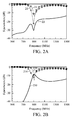
- FIG. 2A is a diagram for illustrating S parameters of an antenna system of a communication device according to a first embodiment of the invention
- FIG. 2B is a diagram for illustrating S parameters of an antenna system of a communication device without any resistive element according to a first embodiment of the invention
- FIG. 3 is a diagram for illustrating antenna efficiency of an antenna system of a communication device according to a first embodiment of the invention
- FIG. 4 is a diagram for illustrating a communication device according to a second embodiment of the invention.
- FIG. 5 is a diagram for illustrating a communication device according to a third embodiment of the invention.
- FIG. 6 is a diagram for illustrating a communication device according to a fourth embodiment of the invention.
- FIG. 7 is a diagram for illustrating a communication device according to a fifth embodiment of the invention.
- FIG. 8 is a diagram for illustrating a communication device according to a sixth embodiment of the invention.
- FIG. 1 is a diagram for illustrating a communication device 100 according to a first embodiment of the invention.
- the communication device 100 may be a smart phone, a tablet computer, or a notebook computer.
- the communication device 100 comprises a ground element 10 and an antenna system.
- the antenna system is adjacent to the ground element 10.
- the antenna system at least comprises a first antenna 11, a second antenna 12, a resistive element 13, and a connection element 14.
- the second antenna 12 is adjacent to the first antenna 11.
- the connection element 14 comprises a first portion 141 and a second portion 142, wherein the first portion 141 is coupled to the first antenna 11, and the second portion 142 is coupled to the second antenna 12.
- the resistive element 13 is coupled between the first portion 141 and the second portion 142 of the connection element 14.
- the first antenna 11 further comprises a first feeding element 111 coupled to a first signal source 112
- the second antenna 12 further comprises a second feeding element 121 coupled to a second signal source 122.
- the communication device 100 further comprises other essential components, such as a dielectric substrate, a processor, a battery, and a housing (not shown).
- FIG. 2A is a diagram for illustrating S parameters of the antenna system of the communication device 100 according to the first embodiment of the invention.
- the ground element 10 has a length of about 120mm and has a width of about 70mm.
- Each of the first antenna 11 and the second antenna 12 has a total size of about 1500mm 3 (30mm by 10mm by 5mm).
- the first antenna 11 and the second antenna 12 both generate resonant modes at a low frequency of about 900MHz to cover a GSM900 band (from about 880MHz to 960MHz).
- the reflection coefficient (S11) curve 21 represents the reflection coefficient (S11) of the first antenna 11.
- the reflection coefficient (S22) curve 22 represents the reflection coefficient (S22) of the second antenna 12.
- the isolation (S21) curve 23 represents the isolation (S21) between the first antenna 11 and the second antenna 12. As shown in FIG. 2A , the first antenna 11 and the second antenna 12 may operate in at least one same mobile communication band. In some embodiments, the resistance of the resistive element 13 is about 300 ⁇ . The resistive element 13 and the connection element 14 can improve the isolation (S21) between the first antenna 11 and the second antenna 12 to the lowest value of about -30dB in the GSM900 band.
- FIG. 2B is a diagram for illustrating S parameters of the antenna system of the communication device 100 without the resistive element 13 according to the first embodiment of the invention.
- the resistive element 13 has been removed from the antenna system.
- the reflection coefficient (S11) curve 210 represents the reflection coefficient (S11) of the first antenna 11.
- the reflection coefficient (S22) curve 220 represents the reflection coefficient (S22) of the second antenna 12.
- the isolation (S21) curve 230 represents the isolation (S21) between the first antenna 11 and the second antenna 12.
- the isolation (S21) between the first antenna 11 and the second antenna 12 is from about -9dB to -11dB in the GSM900 band. According to FIGS.
- the resistive element 13 can effectively absorb the coupling currents between the first antenna 11 and the second antenna 12, thereby improving the isolation between the first antenna 11 and the second antenna 12 very much.
- FIG. 3 is a diagram for illustrating antenna efficiency of the antenna system of the communication device 100 according to the first embodiment of the invention.
- the antenna efficiency curve 31 represents the antenna efficiency of the first antenna 11, and the antenna efficiency curve 32 represents the antenna efficiency of the second antenna 12.
- the first antenna 11 and the second antenna 12 both have high antenna efficiency (including the return loss) in the GSM900 band.
- the invention is suitably applied to a mobile communication device, which comprises multiple antennas therein to provide a variety of functions. The invention not only improves the isolation between the antennas but also maintains high antenna efficiency to meet practical application requirements.
- FIG. 4 is a diagram for illustrating a communication device 400 according to a second embodiment of the invention.
- An antenna system of the communication device 400 comprises a first antenna 41 and a second antenna 42.
- the first antenna 41 further comprises a first shorted element 413
- the second antenna 42 further comprises a second shorted element 423, wherein the first shorted element 413 and the second shorted element 423 are coupled to the ground element 10, respectively.
- a connection element 44 comprises a first portion 441 and a second portion 442, wherein the first portion 441 is coupled to the first shorted element 413, and the second portion 442 is coupled to the second shorted element 423.
- Other features of the communication device 400 in the second embodiment are similar to those in the first embodiment.
- the resistive element 13 is coupled between the first shorted element 413 of the first antenna 41 and the second shorted element 423 of the second antenna 42 so as to absorb the coupling currents between the first antenna 41 and the second antenna 42. Accordingly, the performance of the communication device 400 in the second embodiment is similar to that in the first embodiment.
- FIG. 5 is a diagram for illustrating a communication device 500 according to a third embodiment of the invention.
- the first antenna 41 further comprises a first feeding element 411 and a first shorted element 413
- the second antenna 42 further comprises a second feeding element 421 and a second shorted element 423.
- a connection element 54 comprises a first portion 541 and a second portion 542, wherein the first portion 541 is coupled to the first shorted element 413 of the first antenna 41, and the second portion 542 is coupled to the second feeding element 421 of the second antenna 42.
- Other features of the communication device 500 in the third embodiment are similar to those in the second embodiment.
- the resistive element 13 may have different connection positions but still absorb the coupling currents between the first antenna 41 and the second antenna 42. Accordingly, the performance of the communication device 500 in the third embodiment is similar to that in the first embodiment.
- FIG. 6 is a diagram for illustrating a communication device 600 according to a fourth embodiment of the invention.
- a connection element 64 comprises a first portion 641 and a second portion 642, wherein a vertical projection of the first portion 641 overlaps with the ground element 10, and a vertical projection of the second portion 642 also overlaps with the ground element 10.
- the first portion 641 of the connection element 64 is coupled to the first feeding element 111 of the first antenna 11, and the second portion 642 of the connection element 64 is coupled to the second feeding element 121 of the second antenna 12.
- the connection element 64 and the resistive element 13 are disposed above the ground element 10.
- Other features of the communication device 600 in the fourth embodiment are similar to those in the first embodiment.
- the resistive element 13 can absorb the coupling currents between the first antenna 11 and the second antenna 12. Accordingly, the performance of the communication device 600 in the fourth embodiment is similar to that in the first embodiment.
- FIG. 7 is a diagram for illustrating a communication device 700 according to a fifth embodiment of the invention.
- an antenna system of the communication device 700 is adjacent to a corner of the ground element 10.
- the antenna system comprises a first antenna 71 and a second antenna 72.
- the first antenna 71 and the second antenna 72 are adjacent to two edges of the ground element 10, respectively, wherein the two edges of the ground element 10 are substantially perpendicular to each other.
- a connection element 74 comprises a first portion 741 and a second portion 742, wherein the first portion 741 is coupled to the first antenna 71, and the second portion 742 is coupled to the second antenna 72.
- the connection element 74 and the resistive element 13 may be both coupled between the first antenna 71 and the second antenna 72.
- connection positions of the connection element 74 and the resistive element 13 are not limitations of the invention.
- Other features of the communication device 700 in the fifth embodiment are similar to those in the first embodiment.
- the resistive element 13 can absorb the coupling currents between the first antenna 71 and the second antenna 72. Accordingly, the performance of the communication device 700 in the fifth embodiment is similar to that in the first embodiment.
- FIG. 8 is a diagram for illustrating a communication device 800 according to a sixth embodiment of the invention.
- the first antenna 11 further comprises a first feeding element 811 for transmitting a microwave signal of a first signal source 812 to the first antenna 11
- the second antenna 12 further comprises a second feeding element 821 for transmitting a microwave signal of a second signal source 822 to the second antenna 12.
- the first feeding element 811 and the second feeding element 821 may have a variety of shapes, such as S shapes and L shapes.
- the resistive element 13 is directly coupled between the first feeding element 811 of the first antenna 11 and the second feeding element 821 of the second antenna 12. Note that the resistive element 13 is not coupled through any connection element.
- the resistive element 13 can absorb the coupling currents between the first antenna 11 and the second antenna 12. Accordingly, the performance of the communication device 800 in the sixth embodiment is similar to that in the first embodiment.
Landscapes
- Details Of Aerials (AREA)
- Support Of Aerials (AREA)
Applications Claiming Priority (1)
| Application Number | Priority Date | Filing Date | Title |
|---|---|---|---|
| TW101133609A TWI523324B (zh) | 2012-09-14 | 2012-09-14 | 通訊裝置 |
Publications (2)
| Publication Number | Publication Date |
|---|---|
| EP2709209A1 true EP2709209A1 (fr) | 2014-03-19 |
| EP2709209B1 EP2709209B1 (fr) | 2017-04-05 |
Family
ID=47631368
Family Applications (1)
| Application Number | Title | Priority Date | Filing Date |
|---|---|---|---|
| EP13154045.2A Active EP2709209B1 (fr) | 2012-09-14 | 2013-02-05 | Dispositif de communication et système d'antenne à isolation élevée |
Country Status (3)
| Country | Link |
|---|---|
| US (1) | US9077085B2 (fr) |
| EP (1) | EP2709209B1 (fr) |
| TW (1) | TWI523324B (fr) |
Cited By (3)
| Publication number | Priority date | Publication date | Assignee | Title |
|---|---|---|---|---|
| EP3057176A1 (fr) * | 2015-02-11 | 2016-08-17 | Xiaomi Inc. | Module d'antenne et terminal mobile |
| KR20170083900A (ko) * | 2016-01-11 | 2017-07-19 | 삼성전자주식회사 | 금속 하우징 안테나를 포함한 전자 장치 |
| CN111600129A (zh) * | 2020-05-27 | 2020-08-28 | 西安朗普达通信科技有限公司 | 一种新型多天线系统 |
Families Citing this family (9)
| Publication number | Priority date | Publication date | Assignee | Title |
|---|---|---|---|---|
| FR3021164B1 (fr) * | 2014-05-19 | 2018-05-11 | Centre National De La Recherche Scientifique | Systeme d'antennes pour reduire le couplage electromagnetique entre antennes |
| TWI550954B (zh) * | 2014-12-26 | 2016-09-21 | 瑞昱半導體股份有限公司 | 天線組與天線隔離度增強方法 |
| TWI593167B (zh) * | 2015-12-08 | 2017-07-21 | 財團法人工業技術研究院 | 天線陣列 |
| CN105846078A (zh) * | 2016-05-23 | 2016-08-10 | 北京技德网络技术有限公司 | 提高无线设备不同天线之间隔离度的新方法 |
| US10784572B2 (en) * | 2017-06-02 | 2020-09-22 | Apple Inc. | Electronic device with speaker and antenna isolation |
| CN107658561A (zh) * | 2017-11-06 | 2018-02-02 | 珠海市魅族科技有限公司 | 一种天线装置及终端设备 |
| CN109546311A (zh) * | 2018-12-12 | 2019-03-29 | 维沃移动通信有限公司 | 一种天线结构及通信终端 |
| US10608691B1 (en) * | 2019-01-22 | 2020-03-31 | Google Llc | Compact multiple-input multiple-output (MIMO) antenna module |
| CN216563498U (zh) | 2021-04-30 | 2022-05-17 | 荣耀终端有限公司 | 一种电子元件连接结构以及电子设备 |
Citations (1)
| Publication number | Priority date | Publication date | Assignee | Title |
|---|---|---|---|---|
| EP2466684A1 (fr) * | 2010-12-14 | 2012-06-20 | Centre National de la Recherche Scientifique (C.N.R.S) | Système d'antenne en diversité |
Family Cites Families (4)
| Publication number | Priority date | Publication date | Assignee | Title |
|---|---|---|---|---|
| US4382260A (en) * | 1981-05-11 | 1983-05-03 | International Telephone And Telegraph Corporation | Two channel transmit only antenna |
| US5990838A (en) * | 1996-06-12 | 1999-11-23 | 3Com Corporation | Dual orthogonal monopole antenna system |
| US7911387B2 (en) * | 2007-06-21 | 2011-03-22 | Apple Inc. | Handheld electronic device antennas |
| US7724201B2 (en) * | 2008-02-15 | 2010-05-25 | Sierra Wireless, Inc. | Compact diversity antenna system |
-
2012
- 2012-09-14 TW TW101133609A patent/TWI523324B/zh active
-
2013
- 2013-02-05 EP EP13154045.2A patent/EP2709209B1/fr active Active
- 2013-02-26 US US13/777,587 patent/US9077085B2/en active Active
Patent Citations (1)
| Publication number | Priority date | Publication date | Assignee | Title |
|---|---|---|---|---|
| EP2466684A1 (fr) * | 2010-12-14 | 2012-06-20 | Centre National de la Recherche Scientifique (C.N.R.S) | Système d'antenne en diversité |
Non-Patent Citations (4)
| Title |
|---|
| "Minutes of the SWG 1.1 Meeting Antenna System Aspects", 20 October 2011 (2011-10-20), Lisbon - Portugal, XP055093750, Retrieved from the Internet <URL:http://www.ic1004.org/uploads/Meetings/II MC - Lisbon/Minutes/Minutes_SWG1.1.pdf> [retrieved on 20131216] * |
| DIALLO A ET AL: "Enhanced two-antenna structures for universal mobile telecommunications system diversity terminals", 20080204, vol. 2, no. 1, 4 February 2008 (2008-02-04), pages 93 - 101, XP006030333 * |
| LUXEY C: "Design of multi-antenna systems for UMTS mobile phones", ANTENNAS&PROPAGATION CONFERENCE, 2009. LAPC 2009. LOUGHBOROUGH, IEEE, PISCATAWAY, NJ, USA, 16 November 2009 (2009-11-16), pages 57 - 64, XP031579785, ISBN: 978-1-4244-2720-8 * |
| SAOU-WEN SU ET AL: "Printed two monopole-antenna system with a decoupling neutralization line for 2.4-GHz MIMO applications", MICROWAVE AND OPTICAL TECHNOLOGY LETTERS, vol. 53, no. 9, 16 September 2011 (2011-09-16), pages 2037 - 2043, XP055093717, ISSN: 0895-2477, DOI: 10.1002/mop.26199 * |
Cited By (6)
| Publication number | Priority date | Publication date | Assignee | Title |
|---|---|---|---|---|
| EP3057176A1 (fr) * | 2015-02-11 | 2016-08-17 | Xiaomi Inc. | Module d'antenne et terminal mobile |
| US10186755B2 (en) | 2015-02-11 | 2019-01-22 | Xiaomi Inc. | Antenna module and mobile terminal using the same |
| KR20170083900A (ko) * | 2016-01-11 | 2017-07-19 | 삼성전자주식회사 | 금속 하우징 안테나를 포함한 전자 장치 |
| EP3203577A3 (fr) * | 2016-01-11 | 2017-11-01 | Samsung Electronics Co., Ltd | Dispositif électronique comprenant une antenne à boîtier métallique |
| US10283846B2 (en) | 2016-01-11 | 2019-05-07 | Samsung Electronics Co., Ltd. | Electronic device including metal housing antenna |
| CN111600129A (zh) * | 2020-05-27 | 2020-08-28 | 西安朗普达通信科技有限公司 | 一种新型多天线系统 |
Also Published As
| Publication number | Publication date |
|---|---|
| TW201411941A (zh) | 2014-03-16 |
| US9077085B2 (en) | 2015-07-07 |
| US20140078018A1 (en) | 2014-03-20 |
| TWI523324B (zh) | 2016-02-21 |
| EP2709209B1 (fr) | 2017-04-05 |
Similar Documents
| Publication | Publication Date | Title |
|---|---|---|
| EP2709209A1 (fr) | Dispositif de communication et système d'antenne à isolation élevée | |
| US9190740B2 (en) | Communication device and antennas with high isolation characteristics | |
| US9300055B2 (en) | Mobile device with two antennas and antenna switch modules | |
| EP2448062A2 (fr) | Dispositif de communication et antenne associée | |
| EP3340482B1 (fr) | Ensemble boîtier de terminal, terminal et téléphone mobile | |
| EP3226347B1 (fr) | Antenne wifi | |
| US9455499B2 (en) | Communication device and antenna element therein | |
| US9112269B2 (en) | Communication device and antenna element therein | |
| US10381710B1 (en) | Single feed passive antenna for a metal back cover | |
| US20140266968A1 (en) | Communication device and antenna element therein | |
| CN109509961B (zh) | 移动电子装置 | |
| CN112350053B (zh) | 天线结构及具有该天线结构的无线通信装置 | |
| CN102789590B (zh) | 射频sim卡及具有该射频sim卡的移动通信设备 | |
| EP2728665B1 (fr) | Dispositif de communication et élément d'antenne large bande correspondant | |
| EP2755277B1 (fr) | Dispositif de communication et élément d'antenne correspondant | |
| CN103682626B (zh) | 通信装置 | |
| CN104347925B (zh) | 一种终端设备的天线装置 | |
| US20140340277A1 (en) | Communication device and antenna element therein | |
| US10411326B1 (en) | Single feed passive antenna for a metal back cover | |
| CN101442150A (zh) | 适用于薄型通讯装置的天线 | |
| CN103943940B (zh) | 通信装置 | |
| KR102558250B1 (ko) | 무선 카드단말기에 구비되는 안테나 및 이를 포함하는 무선 카드단말기 | |
| CN205752518U (zh) | 宽频匹配天线 | |
| CN119447819A (zh) | 可折叠的电子设备、控制天线的方法 | |
| CN112510348A (zh) | 天线及电子设备 |
Legal Events
| Date | Code | Title | Description |
|---|---|---|---|
| PUAI | Public reference made under article 153(3) epc to a published international application that has entered the european phase |
Free format text: ORIGINAL CODE: 0009012 |
|
| AK | Designated contracting states |
Kind code of ref document: A1 Designated state(s): AL AT BE BG CH CY CZ DE DK EE ES FI FR GB GR HR HU IE IS IT LI LT LU LV MC MK MT NL NO PL PT RO RS SE SI SK SM TR |
|
| AX | Request for extension of the european patent |
Extension state: BA ME |
|
| 17P | Request for examination filed |
Effective date: 20140919 |
|
| RBV | Designated contracting states (corrected) |
Designated state(s): AL AT BE BG CH CY CZ DE DK EE ES FI FR GB GR HR HU IE IS IT LI LT LU LV MC MK MT NL NO PL PT RO RS SE SI SK SM TR |
|
| GRAP | Despatch of communication of intention to grant a patent |
Free format text: ORIGINAL CODE: EPIDOSNIGR1 |
|
| STAA | Information on the status of an ep patent application or granted ep patent |
Free format text: STATUS: GRANT OF PATENT IS INTENDED |
|
| RIC1 | Information provided on ipc code assigned before grant |
Ipc: H01Q 1/52 20060101AFI20161102BHEP Ipc: H01Q 1/24 20060101ALN20161102BHEP Ipc: H01Q 21/28 20060101ALN20161102BHEP |
|
| INTG | Intention to grant announced |
Effective date: 20161123 |
|
| GRAS | Grant fee paid |
Free format text: ORIGINAL CODE: EPIDOSNIGR3 |
|
| GRAA | (expected) grant |
Free format text: ORIGINAL CODE: 0009210 |
|
| STAA | Information on the status of an ep patent application or granted ep patent |
Free format text: STATUS: THE PATENT HAS BEEN GRANTED |
|
| AK | Designated contracting states |
Kind code of ref document: B1 Designated state(s): AL AT BE BG CH CY CZ DE DK EE ES FI FR GB GR HR HU IE IS IT LI LT LU LV MC MK MT NL NO PL PT RO RS SE SI SK SM TR |
|
| REG | Reference to a national code |
Ref country code: GB Ref legal event code: FG4D |
|
| REG | Reference to a national code |
Ref country code: CH Ref legal event code: EP |
|
| REG | Reference to a national code |
Ref country code: AT Ref legal event code: REF Ref document number: 882610 Country of ref document: AT Kind code of ref document: T Effective date: 20170415 |
|
| REG | Reference to a national code |
Ref country code: IE Ref legal event code: FG4D |
|
| REG | Reference to a national code |
Ref country code: DE Ref legal event code: R096 Ref document number: 602013019326 Country of ref document: DE |
|
| REG | Reference to a national code |
Ref country code: DE Ref legal event code: R082 Ref document number: 602013019326 Country of ref document: DE Representative=s name: MICHALSKI HUETTERMANN & PARTNER PATENTANWAELTE, DE |
|
| REG | Reference to a national code |
Ref country code: NL Ref legal event code: MP Effective date: 20170405 |
|
| REG | Reference to a national code |
Ref country code: LT Ref legal event code: MG4D |
|
| REG | Reference to a national code |
Ref country code: AT Ref legal event code: MK05 Ref document number: 882610 Country of ref document: AT Kind code of ref document: T Effective date: 20170405 |
|
| PG25 | Lapsed in a contracting state [announced via postgrant information from national office to epo] |
Ref country code: NL Free format text: LAPSE BECAUSE OF FAILURE TO SUBMIT A TRANSLATION OF THE DESCRIPTION OR TO PAY THE FEE WITHIN THE PRESCRIBED TIME-LIMIT Effective date: 20170405 |
|
| PG25 | Lapsed in a contracting state [announced via postgrant information from national office to epo] |
Ref country code: HR Free format text: LAPSE BECAUSE OF FAILURE TO SUBMIT A TRANSLATION OF THE DESCRIPTION OR TO PAY THE FEE WITHIN THE PRESCRIBED TIME-LIMIT Effective date: 20170405 Ref country code: LT Free format text: LAPSE BECAUSE OF FAILURE TO SUBMIT A TRANSLATION OF THE DESCRIPTION OR TO PAY THE FEE WITHIN THE PRESCRIBED TIME-LIMIT Effective date: 20170405 Ref country code: GR Free format text: LAPSE BECAUSE OF FAILURE TO SUBMIT A TRANSLATION OF THE DESCRIPTION OR TO PAY THE FEE WITHIN THE PRESCRIBED TIME-LIMIT Effective date: 20170706 Ref country code: FI Free format text: LAPSE BECAUSE OF FAILURE TO SUBMIT A TRANSLATION OF THE DESCRIPTION OR TO PAY THE FEE WITHIN THE PRESCRIBED TIME-LIMIT Effective date: 20170405 Ref country code: NO Free format text: LAPSE BECAUSE OF FAILURE TO SUBMIT A TRANSLATION OF THE DESCRIPTION OR TO PAY THE FEE WITHIN THE PRESCRIBED TIME-LIMIT Effective date: 20170705 Ref country code: ES Free format text: LAPSE BECAUSE OF FAILURE TO SUBMIT A TRANSLATION OF THE DESCRIPTION OR TO PAY THE FEE WITHIN THE PRESCRIBED TIME-LIMIT Effective date: 20170405 Ref country code: AT Free format text: LAPSE BECAUSE OF FAILURE TO SUBMIT A TRANSLATION OF THE DESCRIPTION OR TO PAY THE FEE WITHIN THE PRESCRIBED TIME-LIMIT Effective date: 20170405 |
|
| PG25 | Lapsed in a contracting state [announced via postgrant information from national office to epo] |
Ref country code: IS Free format text: LAPSE BECAUSE OF FAILURE TO SUBMIT A TRANSLATION OF THE DESCRIPTION OR TO PAY THE FEE WITHIN THE PRESCRIBED TIME-LIMIT Effective date: 20170805 Ref country code: PL Free format text: LAPSE BECAUSE OF FAILURE TO SUBMIT A TRANSLATION OF THE DESCRIPTION OR TO PAY THE FEE WITHIN THE PRESCRIBED TIME-LIMIT Effective date: 20170405 Ref country code: BG Free format text: LAPSE BECAUSE OF FAILURE TO SUBMIT A TRANSLATION OF THE DESCRIPTION OR TO PAY THE FEE WITHIN THE PRESCRIBED TIME-LIMIT Effective date: 20170705 Ref country code: SE Free format text: LAPSE BECAUSE OF FAILURE TO SUBMIT A TRANSLATION OF THE DESCRIPTION OR TO PAY THE FEE WITHIN THE PRESCRIBED TIME-LIMIT Effective date: 20170405 Ref country code: RS Free format text: LAPSE BECAUSE OF FAILURE TO SUBMIT A TRANSLATION OF THE DESCRIPTION OR TO PAY THE FEE WITHIN THE PRESCRIBED TIME-LIMIT Effective date: 20170405 Ref country code: LV Free format text: LAPSE BECAUSE OF FAILURE TO SUBMIT A TRANSLATION OF THE DESCRIPTION OR TO PAY THE FEE WITHIN THE PRESCRIBED TIME-LIMIT Effective date: 20170405 |
|
| REG | Reference to a national code |
Ref country code: DE Ref legal event code: R097 Ref document number: 602013019326 Country of ref document: DE |
|
| REG | Reference to a national code |
Ref country code: FR Ref legal event code: PLFP Year of fee payment: 6 |
|
| PG25 | Lapsed in a contracting state [announced via postgrant information from national office to epo] |
Ref country code: RO Free format text: LAPSE BECAUSE OF FAILURE TO SUBMIT A TRANSLATION OF THE DESCRIPTION OR TO PAY THE FEE WITHIN THE PRESCRIBED TIME-LIMIT Effective date: 20170405 Ref country code: SK Free format text: LAPSE BECAUSE OF FAILURE TO SUBMIT A TRANSLATION OF THE DESCRIPTION OR TO PAY THE FEE WITHIN THE PRESCRIBED TIME-LIMIT Effective date: 20170405 Ref country code: DK Free format text: LAPSE BECAUSE OF FAILURE TO SUBMIT A TRANSLATION OF THE DESCRIPTION OR TO PAY THE FEE WITHIN THE PRESCRIBED TIME-LIMIT Effective date: 20170405 Ref country code: EE Free format text: LAPSE BECAUSE OF FAILURE TO SUBMIT A TRANSLATION OF THE DESCRIPTION OR TO PAY THE FEE WITHIN THE PRESCRIBED TIME-LIMIT Effective date: 20170405 Ref country code: CZ Free format text: LAPSE BECAUSE OF FAILURE TO SUBMIT A TRANSLATION OF THE DESCRIPTION OR TO PAY THE FEE WITHIN THE PRESCRIBED TIME-LIMIT Effective date: 20170405 |
|
| PLBE | No opposition filed within time limit |
Free format text: ORIGINAL CODE: 0009261 |
|
| STAA | Information on the status of an ep patent application or granted ep patent |
Free format text: STATUS: NO OPPOSITION FILED WITHIN TIME LIMIT |
|
| PG25 | Lapsed in a contracting state [announced via postgrant information from national office to epo] |
Ref country code: SM Free format text: LAPSE BECAUSE OF FAILURE TO SUBMIT A TRANSLATION OF THE DESCRIPTION OR TO PAY THE FEE WITHIN THE PRESCRIBED TIME-LIMIT Effective date: 20170405 Ref country code: IT Free format text: LAPSE BECAUSE OF FAILURE TO SUBMIT A TRANSLATION OF THE DESCRIPTION OR TO PAY THE FEE WITHIN THE PRESCRIBED TIME-LIMIT Effective date: 20170405 |
|
| 26N | No opposition filed |
Effective date: 20180108 |
|
| PG25 | Lapsed in a contracting state [announced via postgrant information from national office to epo] |
Ref country code: SI Free format text: LAPSE BECAUSE OF FAILURE TO SUBMIT A TRANSLATION OF THE DESCRIPTION OR TO PAY THE FEE WITHIN THE PRESCRIBED TIME-LIMIT Effective date: 20170405 |
|
| REG | Reference to a national code |
Ref country code: CH Ref legal event code: PL |
|
| PG25 | Lapsed in a contracting state [announced via postgrant information from national office to epo] |
Ref country code: MC Free format text: LAPSE BECAUSE OF FAILURE TO SUBMIT A TRANSLATION OF THE DESCRIPTION OR TO PAY THE FEE WITHIN THE PRESCRIBED TIME-LIMIT Effective date: 20170405 |
|
| REG | Reference to a national code |
Ref country code: IE Ref legal event code: MM4A |
|
| REG | Reference to a national code |
Ref country code: BE Ref legal event code: MM Effective date: 20180228 |
|
| PG25 | Lapsed in a contracting state [announced via postgrant information from national office to epo] |
Ref country code: CH Free format text: LAPSE BECAUSE OF NON-PAYMENT OF DUE FEES Effective date: 20180228 Ref country code: LU Free format text: LAPSE BECAUSE OF NON-PAYMENT OF DUE FEES Effective date: 20180205 Ref country code: LI Free format text: LAPSE BECAUSE OF NON-PAYMENT OF DUE FEES Effective date: 20180228 |
|
| PG25 | Lapsed in a contracting state [announced via postgrant information from national office to epo] |
Ref country code: IE Free format text: LAPSE BECAUSE OF NON-PAYMENT OF DUE FEES Effective date: 20180205 |
|
| PG25 | Lapsed in a contracting state [announced via postgrant information from national office to epo] |
Ref country code: BE Free format text: LAPSE BECAUSE OF NON-PAYMENT OF DUE FEES Effective date: 20180228 |
|
| PG25 | Lapsed in a contracting state [announced via postgrant information from national office to epo] |
Ref country code: MT Free format text: LAPSE BECAUSE OF NON-PAYMENT OF DUE FEES Effective date: 20180205 |
|
| PG25 | Lapsed in a contracting state [announced via postgrant information from national office to epo] |
Ref country code: TR Free format text: LAPSE BECAUSE OF FAILURE TO SUBMIT A TRANSLATION OF THE DESCRIPTION OR TO PAY THE FEE WITHIN THE PRESCRIBED TIME-LIMIT Effective date: 20170405 |
|
| PG25 | Lapsed in a contracting state [announced via postgrant information from national office to epo] |
Ref country code: HU Free format text: LAPSE BECAUSE OF FAILURE TO SUBMIT A TRANSLATION OF THE DESCRIPTION OR TO PAY THE FEE WITHIN THE PRESCRIBED TIME-LIMIT; INVALID AB INITIO Effective date: 20130205 Ref country code: PT Free format text: LAPSE BECAUSE OF FAILURE TO SUBMIT A TRANSLATION OF THE DESCRIPTION OR TO PAY THE FEE WITHIN THE PRESCRIBED TIME-LIMIT Effective date: 20170405 |
|
| PG25 | Lapsed in a contracting state [announced via postgrant information from national office to epo] |
Ref country code: MK Free format text: LAPSE BECAUSE OF NON-PAYMENT OF DUE FEES Effective date: 20170405 Ref country code: CY Free format text: LAPSE BECAUSE OF FAILURE TO SUBMIT A TRANSLATION OF THE DESCRIPTION OR TO PAY THE FEE WITHIN THE PRESCRIBED TIME-LIMIT Effective date: 20170405 |
|
| PG25 | Lapsed in a contracting state [announced via postgrant information from national office to epo] |
Ref country code: AL Free format text: LAPSE BECAUSE OF FAILURE TO SUBMIT A TRANSLATION OF THE DESCRIPTION OR TO PAY THE FEE WITHIN THE PRESCRIBED TIME-LIMIT Effective date: 20170405 |
|
| PGFP | Annual fee paid to national office [announced via postgrant information from national office to epo] |
Ref country code: GB Payment date: 20260112 Year of fee payment: 14 |
|
| PGFP | Annual fee paid to national office [announced via postgrant information from national office to epo] |
Ref country code: DE Payment date: 20260107 Year of fee payment: 14 |
|
| PGFP | Annual fee paid to national office [announced via postgrant information from national office to epo] |
Ref country code: FR Payment date: 20260108 Year of fee payment: 14 |