EP2709253A2 - Temperaturkompensation eines Sperrwandlers - Google Patents
Temperaturkompensation eines Sperrwandlers Download PDFInfo
- Publication number
- EP2709253A2 EP2709253A2 EP20130275116 EP13275116A EP2709253A2 EP 2709253 A2 EP2709253 A2 EP 2709253A2 EP 20130275116 EP20130275116 EP 20130275116 EP 13275116 A EP13275116 A EP 13275116A EP 2709253 A2 EP2709253 A2 EP 2709253A2
- Authority
- EP
- European Patent Office
- Prior art keywords
- voltage
- temperature
- converter
- ref
- ptat
- Prior art date
- Legal status (The legal status is an assumption and is not a legal conclusion. Google has not performed a legal analysis and makes no representation as to the accuracy of the status listed.)
- Granted
Links
Images


Classifications
-
- H—ELECTRICITY
- H02—GENERATION; CONVERSION OR DISTRIBUTION OF ELECTRIC POWER
- H02M—APPARATUS FOR CONVERSION BETWEEN AC AND AC, BETWEEN AC AND DC, OR BETWEEN DC AND DC, AND FOR USE WITH MAINS OR SIMILAR POWER SUPPLY SYSTEMS; CONVERSION OF DC OR AC INPUT POWER INTO SURGE OUTPUT POWER; CONTROL OR REGULATION THEREOF
- H02M3/00—Conversion of DC power input into DC power output
- H02M3/02—Conversion of DC power input into DC power output without intermediate conversion into AC
- H02M3/04—Conversion of DC power input into DC power output without intermediate conversion into AC by static converters
- H02M3/10—Conversion of DC power input into DC power output without intermediate conversion into AC by static converters using discharge tubes with control electrode or semiconductor devices with control electrode
- H02M3/145—Conversion of DC power input into DC power output without intermediate conversion into AC by static converters using discharge tubes with control electrode or semiconductor devices with control electrode using devices of a triode or transistor type requiring continuous application of a control signal
- H02M3/155—Conversion of DC power input into DC power output without intermediate conversion into AC by static converters using discharge tubes with control electrode or semiconductor devices with control electrode using devices of a triode or transistor type requiring continuous application of a control signal using semiconductor devices only
- H02M3/156—Conversion of DC power input into DC power output without intermediate conversion into AC by static converters using discharge tubes with control electrode or semiconductor devices with control electrode using devices of a triode or transistor type requiring continuous application of a control signal using semiconductor devices only with automatic control of output voltage or current, e.g. switching regulators
-
- H—ELECTRICITY
- H02—GENERATION; CONVERSION OR DISTRIBUTION OF ELECTRIC POWER
- H02M—APPARATUS FOR CONVERSION BETWEEN AC AND AC, BETWEEN AC AND DC, OR BETWEEN DC AND DC, AND FOR USE WITH MAINS OR SIMILAR POWER SUPPLY SYSTEMS; CONVERSION OF DC OR AC INPUT POWER INTO SURGE OUTPUT POWER; CONTROL OR REGULATION THEREOF
- H02M3/00—Conversion of DC power input into DC power output
- H02M3/22—Conversion of DC power input into DC power output with intermediate conversion into AC
- H02M3/24—Conversion of DC power input into DC power output with intermediate conversion into AC by static converters
- H02M3/28—Conversion of DC power input into DC power output with intermediate conversion into AC by static converters using discharge tubes with control electrode or semiconductor devices with control electrode to produce the intermediate AC
- H02M3/325—Conversion of DC power input into DC power output with intermediate conversion into AC by static converters using discharge tubes with control electrode or semiconductor devices with control electrode to produce the intermediate AC using devices of a triode or a transistor type requiring continuous application of a control signal
- H02M3/335—Conversion of DC power input into DC power output with intermediate conversion into AC by static converters using discharge tubes with control electrode or semiconductor devices with control electrode to produce the intermediate AC using devices of a triode or a transistor type requiring continuous application of a control signal using semiconductor devices only
Definitions
- This invention relates to flyback converters and in particular to DC-DC flyback converters and to a temperature compensation technique for an isolated flyback converter, where the converter uses an output diode and primary side sensing to detect an output voltage.
- DC-DC flyback converters are well known.
- the output voltage can be sensed by various methods for providing feedback.
- One way to convey the output voltage to the primary side while maintaining isolation is to use an optocoupler.
- using an optocoupler requires additional circuitry, space, power, and cost.
- a more elegant way of detecting the output voltage is to sense a voltage at a terminal of the power switch when the power switch is turned off during the discharge (or flyback) cycle of the converter. Such a sensed voltage is related in a known manner to the output voltage.
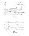
- Fig. 1 illustrates one type of flyback converter which detects the output voltage V OUT by detecting the voltage at the primary winding L1 of the transformer T1 when the power switch MOSFET M POWER is turned off during the discharge (or flyback) cycle. Sensing an output voltage by a signal at the primary side of a transformer is sometimes referred to as primary side sensing.
- the MOSFET M POWER is controlled by an output regulation and control circuit 14 to connect the primary winding L1 between the input voltage V IN (e.g., a battery voltage) and ground during a charging cycle.
- V IN e.g., a battery voltage
- the MOSFET M POWER is turned off after a controlled time, and the Schottky diode D becomes forward biased.
- a conventional pn diode may also be used.
- the current through the secondary winding L2 is transferred to the load and the smoothing capacitor C OUT at the required voltage.
- the circuit 14 detects the voltage at the drain of MOSFET M POWER during the discharge cycle (MOSFET M POWER is off).
- the drain voltage is related to the winding ratio of L1 and L2, and the voltage across winding L2 is the output voltage Vout plus the voltage drop across the diode D.
- Such primary side sensing circuits for detecting V OUT are well known and need not be described in detail.
- the full data sheet for the Linear Technology LT3573 flyback converter incorporated herein by reference and available on-line, describes the operation of the feedback circuit. This operation is also described in US Patent Nos. 7,471,522 and 7,463,497 , assigned to the present assignee and incorporated herein by reference. Other known primary side voltage sensing techniques may be used.
- the circuit 14 continues to control the duty cycle of the MOSFET M POWER , at a variable frequency or a fixed frequency, to regulate V OUT based on the sensed voltage.
- the output regulation and control circuit 14 may use any type of conventional technique to regulate, including current mode, voltage mode, or other modes.
- a voltage mode converter is shown.
- the switch voltage Vsw at the drain of the MOSFET M POWER is sensed by an output voltage sense circuit 16.
- the circuit 16 includes a circuit that subtracts V IN from Vsw (to obtain the voltage across the winding L1) then scales the voltage to generate a feedback voltage V FB , wherein, when V FB equals a reference voltage V REF , the output voltage V OUT is at the desired value, such as 5 volts.
- V FB V OUT + V F T ⁇ N P N S ⁇ Kp
- V F (T) the forward voltage drop of diode D
- N P /N S is the turns ratio of L1 and L2
- Kp is a proportion defined by a resistor divider.
- the voltage drop across the diode D has a negative temperature coefficient and is about -2mV/K. Since the converter adjusts the duty cycle of MOSFET M POWER to keep V FB equal to V REF , the output voltage V OUT becomes higher than the desired voltage as the temperature rises.
- V FB is sampled by a sample and hold circuit 18, and the sampled V FB is applied to one input of an error amplifier 20.
- the error amplifier 20 compares V FB to a reference voltage V REF and outputs an error voltage V E .
- a pulse generator 22 sets the duty cycle of the MOSFET M POWER to cause the error voltage V E to approximately equal zero. In this way the output voltage V OUT is regulated, albeit temperature dependent.
- the pulse generator 22 may include a current source that charges a capacitor based the value of V E to create a threshold voltage, a ramp generator, a PWM comparator that compares the threshold voltage to the ramp for setting the duty cycle, and drive circuitry for the MOSFET M POWER . Such circuitry is conventional.
- Fig. 2 illustrates the current through the primary winding L1, the current through the secondary winding L2, and the voltage V SW across the MOSFET M POWER for a particular duty cycle.
- the MOSFET M POWER turns on to charge the primary winding L1, causing a ramping current to flow in winding L1.
- the diode D is not conducting at this time.
- MOSFET M POWER shuts off and the diode D conducts. This ceases current in the primary winding L1 and causes the current through the secondary winding L2 to ramp down while charging the output capacitor C OUT and providing current to the load.
- the voltage across the MOSFET M POWER is related to the output voltage V OUT and is sampled during this time by the circuit 14.
- MOSFET M POWER turns on again, and the cycle repeats.
- Fig. 3 illustrates a conventional isolated flyback converter where the primary side sensing is implemented with a third winding L3, having N B turns, also referred to as a bias winding.
- a voltage will be generated across the third winding L3.
- the circuit formed of capacitor C BIAS and diode D BIAS limits spikes.
- the voltage V B is sensed by the output voltage sense circuit and scaled to generate the feedback voltage V FB in accordance with the following equation, previously described.
- V FB V OUT + V F T ⁇ N B N S ⁇ Kp
- Fig. 4 illustrates a prior art circuit within the output voltage sense circuit 16 of Fig. 1 that subtracts the V IN voltage from the V SW voltage and scales down the voltage with resistors R P1 and R P2 .
- current source 24 draws a current through the p-channel MOSFET M1, having its source connected to V IN .
- the p-channel MOSFETs M1 and M2 have their gates connected so that the source of MOSFET M2 is at V IN , assuming equal threshold voltages. This subtracts V IN from V SW . Since the converter adjusts the duty cycle to keep V FB matched to V REF , the current through the resistor R P2 must be controlled, by adjusting V SW , to produce V REF .
- the user selects the resistor R P1 needed to scale V FB to generate the desired output voltage and connects the resistor R P1 to a terminal of the package housing the converter control circuit 14.
- R P2 may be 10K ohms and formed on the same chip as the converter control circuit 14.
- Fig. 5 illustrates a prior art circuit within the output voltage sense circuit 16 of Fig. 3 that scales down the voltage V B with resistors R B1 and R B2 .
- V F (T) in the various equations varies with temperature, and V OUT is directly set by V FB , V OUT slopes upward with temperature, as shown in Fig. 6 .
- V OUT has a positive temperature coefficient.
- V OUT is only accurate at room temperature. In some environments, V OUT varies as much as 300mV during the operation of the converter due to temperature changes. This is very significant when the nominal V OUT is 5 V or 3.3 V.
- Figs. 7 and 8 illustrate prior art temperature compensation circuits added to the circuits of Figs. 4 and 5 , respectively.
- a conventional bandgap voltage generator provides a stable reference voltage V REF to the base of the bipolar transistor 28.
- the V BE of the transistor 28 has a negative temperature coefficient of about -2mV/K.
- the voltage at the emitter of the transistor 28 is across the temperature compensation resistor R TC , which is an external (off-chip) resistor selected by the user.
- the current through the transistor 28 and through the MOSFET M4 is thus set by the value of R TC and the changing V BE with temperature.
- MOSFET M3 is connected as a current mirror and adds a variable current I TC to the V FB node.
- the negative temperature coefficient of V F (T) is offset by the positive temperature coefficient of the current I TC .
- the main problem with the temperature compensation circuits of Figs, 7 and 8 is that the user first selects R P1 to generate the desired V OUT at room temperature, then the user heats up the converter to determine the slope of V OUT vs. temperature. Then the user selects R TC to offset the V OUT slope (i.e., makes it independent of temperature).
- the I TC current is always applied as a bias current to the V FB node, the selection of R TC changes V FB , even at room temperature, requiring the user to select a different R P1 to achieve the desired V OUT .
- the more iterations performed, the more optimal the selection of R P1 and R TC This is a tedious process that still results in non-optimized R P1 and R TC values.
- a temperature compensation technique for an isolated flyback converter using primary side sensing and an output diode is disclosed.
- a voltage source generating a proportional-to-absolute temperature voltage V PTAT is connected to the V FB node of a feedback loop in the converter via a temperature compensation resistor R TC .
- V PTAT is selected to equal a reference voltage V REF at an initial calibration temperature, such as room temperature.
- the user selects a scaling resistor in the feedback loop of the converter at room temperature so that, when the desired V OUT is achieved, V FB equals V REF . Since the converter controls V FB to be equal to V REF during operation at room temperature, there is no current through the resistor R TC at the time that the user selects the scaling resistor. Therefore, the temperature compensation circuit has no effect on the converter at room temperature.
- the temperature of the converter is raised to determine the slope of V OUT as V OUT rises with temperature.
- the optimal value of resistor R TC is then selected as the R TC value that offsets the slope of V OUT . This may be done using a potentiometer. Alternatively, if the diode drop vs. temperature of the output diode is already known, the proper value of R TC may be determined by equations without raising the temperature of the converter. The selection of R TC does not affect V OUT at room temperature, so there is no need to tweak the scaling resistor after R TC is selected. Accordingly, optimal values of the scaling resistor and the temperature compensation resistor R TC may be selected without an iterative process, greatly easing the user's task and improving performance of the converter with temperature.
- V PTAT voltage source Various techniques of forming the V PTAT voltage source are described.
- the flyback converter and scaling circuits may be conventional.
- the invention is shown being used in conjunction with the various prior art circuits of Figs. 1 and 3-5.
- the invention may be used in conjunction with virtually every type of feedback circuit in an isolated flyback converter using primary side sensing.
- Fig. 9 illustrates a temperature compensation circuit 30 connected to the V FB node of the circuit of Fig. 4 .
- a voltage source 32 generates a voltage that is proportional to temperature. Such a voltage is referred to as a proportional-to-absolute temperature voltage V PTAT .
- the voltage source 32 is connected via a temperature compensation (TC) resistor R TC to the V FB node 34 in a feedback loop of an isolated flyback converter using primary side sensing.
- the converter may be, for example, either of the converters of Fig. 1 or Fig. 3 , and the temperature compensation circuit 30 may be connected to an input of the error amplifier 20 or other differential amplifier that compares the V FB to a reference voltage V REF in order to adjust the duty cycle of a power switch to cause V FB to match V REF .
- the resistor R TC is typically external to a chip containing the control circuit 14 ( Fig. 1 ) and is connected to a pin of the IC package. The user selects the proper resistor R TC based on the particular components used in the converter.
- the TC circuit 30 is configured to generate zero current (or substantially zero current) through the resistor R TC at room temperature, assuming the initial scaling is performed at room temperature for setting V OUT . Since the feedback loop causes the converter to always match V FB to V REF (shown in Fig. 1 ) at the input to the error amplifier 20, V PTAT is set to be V REF at room temperature. Accordingly, since the same voltage is applied to both sides of the resistor R TC , there will be no current through R TC , and the setting of the scaling resistor in the feedback loop will be independent of the TC circuit 30.
- step 38 of Fig. 15 the converter is operated at room temperature. At this temperature, the TC circuit 30 has no effect on V OUT .
- the scaling resistor R P1 is selected by the user to cause V FB to equal V REF when V OUT is at the desired value, such as 5 V.
- the selection of the scaling resistor R B1 may use empirical methods for the highest accuracy. Therefore, the scaling resistor R P1 is set to its optimal value in only one step.
- the scaling resistor R P1 is external to the converter control chip and connected to a pin of the IC package.
- the scaling resistor may be any resistive element in any type of feedback loop, such as any resistor in a resistor divider circuit.
- the scaling resistor may even be an adjustable resistance on the same chip as the control circuit 14. In another embodiment, either or both of resistors R P1 and R P2 may be adjusted to achieve the desired V OUT .
- the TC resistor R TC plays no part in the setting of V OUT at room temperature (T 0 ).
- step 42 if the optimal value of R TC is to be determined empirically, V OUT is monitored while the temperature of the converter is increased to determine V OUT vs. temperature. V OUT will increase with temperature due to the voltage drop across the output diode decreasing with temperature. In other words, V SW is no longer representing the desired V OUT level while the current through the resistor R P2 is generating a V FB equal to V REF ( Fig. 1 ). What is needed, therefore, is for the TC circuit 30 to add some current through resistor R P2 to cause V FB to equal V REF and lower Vsw (and V OUT ) to the desired level.
- the V PTAT generated by the voltage source 32 increases with temperature and thus increases a current through R TC with an increase in temperature.
- the amount of the current increase is proportional to the value of R TC .
- the value of RTC may be adjusted during the ramping of the temperature, such as with a potentiometer, to offset the slope of V OUT .
- the proper R TC value may be determined through calculations if the diode drop vs. temperature of the output diode D is already known. In such a case, the converter does not have to be heated.
- step 44 the desired value of the TC resistor R TC to offset the slope of V OUT is obtained.
- Fig. 10 illustrates V OUT vs. temperature without any temperature compensation (solid line) and also with the effects of the TC circuit 30 (dashed lines). The effects of selecting too high an R TC value, too low an R TC value, and an optimal R TC value are shown.
- step 46 the optimal TC resistor R TC is connected to the appropriate pin of the IC package containing the control circuit 14 and the TC circuit 30 to offset the slope of V OUT vs. temperature.
- the effect of the TC circuit 30 does not change V OUT at the calibration temperature T 0 , so the scaling resistor R P1 remains optimal.
- step 48 the converter may be operated over a range of temperatures while V OUT remains substantially stable despite a varying voltage drop across the output diode D.
- Fig. 11 illustrates the TC circuit 30 connected to the circuit of Fig. 5 for a converter ( Fig. 3 ) using a third (or bias) winding for primary side sensing.
- the process for selecting R B1 and R TC are similar to that described with respect to Figs. 9 and 15 .
- V OUT V REF ⁇ N S N B ⁇ R B ⁇ 1 + R B ⁇ 2 R B ⁇ 2 - V F T 0
- the selection of the optimal R B1 is independent of the TC circuit 30 since the TC circuit 30 generates zero current through the TC resistor R TC at room temperature.
- the selection of the scaling resistor R B1 may use empirical methods for the highest accuracy. The user then connects the selected resistor R B1 to the appropriate pin of the IC package containing the converter control circuit and the TC circuit 30.
- Figs. 12 and 13 illustrate one embodiment of the temperature compensation circuit 30, connected to the circuits of Figs. 4 and 5 , respectively, for providing a proportional-to-absolute temperature voltage V PTAT at the TC resistor R TC that is equal to V REF at an initial calibration temperature, such as room temperature.
- a feedback loop consisting of the high gain differential amplifier 38 and MOSFET M5 causes the voltage at the inverting input of the amplifier 38 to be substantially equal to V PTAT , applied to the non-inverting input of the amplifier 38.
- a current source 36 draws a relatively low fixed current I 0 through the MOSFET M5 for proper operation of the feedback loop.
- the voltage applied to the R TC node will be V PTAT .
- Fig. 14 illustrates a suitable voltage source 32 for generating a proportional-to-absolute temperature voltage V PTAT that is equal to V REF at an initial calibration temperature, such as room temperature.
- V BIAS voltage is applied to the base of the bipolar transistor 40, which draws a current through the resistor R 1 . Since the V BE of the transistor 40 is related to the temperature (same temperature as the output diode D), and the current through resistor R 1 equals (V BIAS -V BE )/R 1 , the current is directly related to the temperature.
- the output diode D and the transistor 40 are preferably thermally coupled, such as being in the same chip, so that the base-emitter diode temperature is approximately the same as the output diode temperature.
- the entire voltage source 32 will be on the same IC chip as the control circuit 14 ( Fig. 1 ) and the output diode D for good thermal coupling between the transistor 40 ( Fig. 14 ) and the output diode D.
- the current through the resistor R 1 is mirrored by the configuration of MOSFETs M6 and M7, and the current flows through resistor R 2 .
- the values of either R 1 or R 2 , or both, are selected so that V PTAT equals V REF ( Fig. 1 ) at room temperature (or other calibration temperature of the converter).
- the value of V PTAT rises with temperature proportional to the V BE drop of the transistor 40.
- V PTAT Many other ways to generate V PTAT are also envisioned.
Landscapes
- Engineering & Computer Science (AREA)
- Power Engineering (AREA)
- Dc-Dc Converters (AREA)
Applications Claiming Priority (1)
| Application Number | Priority Date | Filing Date | Title |
|---|---|---|---|
| US13/552,360 US9019727B2 (en) | 2012-07-18 | 2012-07-18 | Temperature compensation of output diode in an isolated flyback converter |
Publications (3)
| Publication Number | Publication Date |
|---|---|
| EP2709253A2 true EP2709253A2 (de) | 2014-03-19 |
| EP2709253A3 EP2709253A3 (de) | 2015-06-03 |
| EP2709253B1 EP2709253B1 (de) | 2016-11-16 |
Family
ID=48463898
Family Applications (1)
| Application Number | Title | Priority Date | Filing Date |
|---|---|---|---|
| EP13275116.5A Active EP2709253B1 (de) | 2012-07-18 | 2013-05-14 | Temperaturkompensation eines Sperrwandlers |
Country Status (4)
| Country | Link |
|---|---|
| US (1) | US9019727B2 (de) |
| EP (1) | EP2709253B1 (de) |
| CN (1) | CN103580489B (de) |
| TW (1) | TWI481177B (de) |
Families Citing this family (13)
| Publication number | Priority date | Publication date | Assignee | Title |
|---|---|---|---|---|
| EP2961246B1 (de) * | 2014-06-26 | 2016-12-21 | Dialog Semiconductor (UK) Limited | LED-Netzspannungsmessung mit einem Stromspiegel |
| US9774324B2 (en) | 2014-12-05 | 2017-09-26 | Intel Corporation | Biasing scheme for high voltage circuits using low voltage devices |
| US9704591B2 (en) * | 2014-12-17 | 2017-07-11 | Sandisk Technologies Llc | Temperature independent reference current generation for calibration |
| US20160179113A1 (en) * | 2014-12-17 | 2016-06-23 | Sandisk Technologies Inc. | Temperature Independent Reference Current Generation For Calibration |
| TWI613542B (zh) | 2016-01-12 | 2018-02-01 | 智原科技股份有限公司 | 電源開啟重置電路 |
| US10852197B2 (en) * | 2018-04-09 | 2020-12-01 | Nxp Usa, Inc. | Temperature sensor in an integrated circuit having offset cancellation |
| US10794982B2 (en) * | 2018-11-21 | 2020-10-06 | Nxp Usa, Inc. | Dynamic calibration of current sense for switching converters |
| CN111446511B (zh) * | 2019-01-17 | 2021-09-03 | 太普动力新能源(常熟)股份有限公司 | 电池及对其电芯进行充电的方法 |
| TWI716323B (zh) * | 2019-06-04 | 2021-01-11 | 極創電子股份有限公司 | 電壓產生器 |
| EP3754850A1 (de) * | 2019-06-18 | 2020-12-23 | TE Connectivity Norge AS | Sensoranordnung zur messung des füllstands einer flüssigkeit |
| CN112583274A (zh) * | 2019-09-30 | 2021-03-30 | 半导体组件工业公司 | 电源转换器以及用于控制电源转换器的方法和控制器 |
| CN111431411B (zh) * | 2020-03-05 | 2021-02-05 | 深圳市创芯微微电子有限公司 | 温度补偿电路、功率控制芯片和电源适配器 |
| CN115021562B (zh) * | 2022-08-04 | 2022-11-04 | 深圳市微源半导体股份有限公司 | 驱动芯片及其控制方法、电子设备 |
Citations (5)
| Publication number | Priority date | Publication date | Assignee | Title |
|---|---|---|---|---|
| US5481178A (en) | 1993-03-23 | 1996-01-02 | Linear Technology Corporation | Control circuit and method for maintaining high efficiency over broad current ranges in a switching regulator circuit |
| US6127815A (en) | 1999-03-01 | 2000-10-03 | Linear Technology Corp. | Circuit and method for reducing quiescent current in a switching regulator |
| US6307356B1 (en) | 1998-06-18 | 2001-10-23 | Linear Technology Corporation | Voltage mode feedback burst mode circuit |
| US7463497B2 (en) | 2006-08-07 | 2008-12-09 | Linear Technology Corporation | Regulator for isolated flyback power supply using primary side sensing |
| US7471522B2 (en) | 2006-08-03 | 2008-12-30 | Linear Technology Corporation | Light load regulator for isolated flyback converter |
Family Cites Families (12)
| Publication number | Priority date | Publication date | Assignee | Title |
|---|---|---|---|---|
| US4633165A (en) | 1984-08-15 | 1986-12-30 | Precision Monolithics, Inc. | Temperature compensated voltage reference |
| US5442534A (en) * | 1993-02-23 | 1995-08-15 | California Institute Of Technology | Isolated multiple output Cuk converter with primary input voltage regulation feedback loop decoupled from secondary load regulation loops |
| EP0954899A2 (de) * | 1997-01-24 | 1999-11-10 | Fische, LLC | Hocheffizienter stromrichter |
| DE19948903C2 (de) * | 1999-10-11 | 2002-07-18 | Infineon Technologies Ag | Getaktete Stromversorgung |
| JP3661666B2 (ja) * | 2001-08-10 | 2005-06-15 | 株式会社村田製作所 | 絶縁型スイッチング電源装置 |
| US7635956B2 (en) * | 2006-01-06 | 2009-12-22 | Active-Semi, Inc. | Primary side constant output voltage controller |
| TW200849784A (en) * | 2007-06-12 | 2008-12-16 | Vastview Tech Inc | DC-DC converter with temperature compensation circuit |
| CN201352719Y (zh) * | 2008-12-31 | 2009-11-25 | 佛山市顺德区瑞德电子实业有限公司 | 一种带自动温度补偿功能的电动车充电器 |
| TWI382641B (zh) * | 2009-07-22 | 2013-01-11 | Richpower Microelectronics | 返馳電源轉換器的二次側電路以及穩定返馳電源轉換器的輸出電流的方法 |
| CN101997433B (zh) * | 2009-08-13 | 2015-01-28 | 上海立隆微电子有限公司 | 反激电源转换器的二次侧电路 |
| US8344793B2 (en) * | 2011-01-06 | 2013-01-01 | Rf Micro Devices, Inc. | Method of generating multiple current sources from a single reference resistor |
| CN102290995B (zh) * | 2011-07-16 | 2013-09-25 | 西安电子科技大学 | 反激式变换器中整流二极管温度补偿电路 |
-
2012
- 2012-07-18 US US13/552,360 patent/US9019727B2/en active Active
-
2013
- 2013-04-30 TW TW102115531A patent/TWI481177B/zh active
- 2013-05-14 EP EP13275116.5A patent/EP2709253B1/de active Active
- 2013-05-27 CN CN201310201189.6A patent/CN103580489B/zh active Active
Patent Citations (6)
| Publication number | Priority date | Publication date | Assignee | Title |
|---|---|---|---|---|
| US5481178A (en) | 1993-03-23 | 1996-01-02 | Linear Technology Corporation | Control circuit and method for maintaining high efficiency over broad current ranges in a switching regulator circuit |
| US6304066B1 (en) | 1993-03-23 | 2001-10-16 | Linear Technology Corporation | Control circuit and method for maintaining high efficiency over broad current ranges in a switching regular circuit |
| US6307356B1 (en) | 1998-06-18 | 2001-10-23 | Linear Technology Corporation | Voltage mode feedback burst mode circuit |
| US6127815A (en) | 1999-03-01 | 2000-10-03 | Linear Technology Corp. | Circuit and method for reducing quiescent current in a switching regulator |
| US7471522B2 (en) | 2006-08-03 | 2008-12-30 | Linear Technology Corporation | Light load regulator for isolated flyback converter |
| US7463497B2 (en) | 2006-08-07 | 2008-12-09 | Linear Technology Corporation | Regulator for isolated flyback power supply using primary side sensing |
Also Published As
| Publication number | Publication date |
|---|---|
| US20140022823A1 (en) | 2014-01-23 |
| CN103580489A (zh) | 2014-02-12 |
| EP2709253B1 (de) | 2016-11-16 |
| EP2709253A3 (de) | 2015-06-03 |
| US9019727B2 (en) | 2015-04-28 |
| CN103580489B (zh) | 2016-10-05 |
| TWI481177B (zh) | 2015-04-11 |
| TW201406032A (zh) | 2014-02-01 |
Similar Documents
| Publication | Publication Date | Title |
|---|---|---|
| US9019727B2 (en) | Temperature compensation of output diode in an isolated flyback converter | |
| US6366068B1 (en) | Switching power supply with overcurrent protection and method | |
| US7605573B2 (en) | Switching regulator providing slope compensation and voltage control method thereof | |
| US7659706B2 (en) | Current detector circuit and current-mode DC-DC converter using same | |
| US7817447B2 (en) | Accurate voltage regulation of a primary-side regulation power supply in continuous conduction mode operation | |
| US7813150B2 (en) | Compensation for parameter variations in a feedback circuit | |
| US20140032942A1 (en) | Voltage regulator, semiconductor device, and data processing system | |
| US20130187619A1 (en) | Shunt regulator | |
| US11218077B2 (en) | Soft-start for isolated power converter | |
| US20070182395A1 (en) | Switching regulator | |
| US20100052627A1 (en) | Dc/dc converter | |
| US6528976B1 (en) | Fet sensing programmable active droop for power supplies | |
| US5917312A (en) | System and method for voltage positioning a regulator and regulator employing the same | |
| US9190918B2 (en) | Controllers and related control methods for generating signals representing an output current to a load in a switched mode power supply | |
| US20120146609A1 (en) | Switching control circuit | |
| US11353904B2 (en) | Multi-slope startup voltage regulator system | |
| US7558084B2 (en) | Switching mode power supply with compensated propagation delay | |
| US20120146604A1 (en) | Switching control circuit | |
| US20110101954A1 (en) | Reference signal generator and method for providing a reference signal with an adaptive temperature coefficient | |
| US8432147B2 (en) | Method of forming a switching regulator and structure therefor | |
| US7781921B2 (en) | Voltage regulator and method for generating indicator signal in voltage regulator | |
| US20090160418A1 (en) | Dc-dc converter | |
| JP2001333571A (ja) | 駆動信号供給回路 | |
| US20080315849A1 (en) | Power Converter and Method for Power Conversion | |
| US12095380B2 (en) | Integrated circuit and power supply circuit |
Legal Events
| Date | Code | Title | Description |
|---|---|---|---|
| PUAI | Public reference made under article 153(3) epc to a published international application that has entered the european phase |
Free format text: ORIGINAL CODE: 0009012 |
|
| AK | Designated contracting states |
Kind code of ref document: A2 Designated state(s): AL AT BE BG CH CY CZ DE DK EE ES FI FR GB GR HR HU IE IS IT LI LT LU LV MC MK MT NL NO PL PT RO RS SE SI SK SM TR |
|
| AX | Request for extension of the european patent |
Extension state: BA ME |
|
| PUAL | Search report despatched |
Free format text: ORIGINAL CODE: 0009013 |
|
| AK | Designated contracting states |
Kind code of ref document: A3 Designated state(s): AL AT BE BG CH CY CZ DE DK EE ES FI FR GB GR HR HU IE IS IT LI LT LU LV MC MK MT NL NO PL PT RO RS SE SI SK SM TR |
|
| AX | Request for extension of the european patent |
Extension state: BA ME |
|
| RIC1 | Information provided on ipc code assigned before grant |
Ipc: H02M 3/156 20060101AFI20150429BHEP Ipc: H02M 3/335 20060101ALI20150429BHEP |
|
| 17P | Request for examination filed |
Effective date: 20151203 |
|
| RBV | Designated contracting states (corrected) |
Designated state(s): AL AT BE BG CH CY CZ DE DK EE ES FI FR GB GR HR HU IE IS IT LI LT LU LV MC MK MT NL NO PL PT RO RS SE SI SK SM TR |
|
| GRAP | Despatch of communication of intention to grant a patent |
Free format text: ORIGINAL CODE: EPIDOSNIGR1 |
|
| INTG | Intention to grant announced |
Effective date: 20160601 |
|
| GRAS | Grant fee paid |
Free format text: ORIGINAL CODE: EPIDOSNIGR3 |
|
| GRAA | (expected) grant |
Free format text: ORIGINAL CODE: 0009210 |
|
| AK | Designated contracting states |
Kind code of ref document: B1 Designated state(s): AL AT BE BG CH CY CZ DE DK EE ES FI FR GB GR HR HU IE IS IT LI LT LU LV MC MK MT NL NO PL PT RO RS SE SI SK SM TR |
|
| REG | Reference to a national code |
Ref country code: GB Ref legal event code: FG4D |
|
| REG | Reference to a national code |
Ref country code: CH Ref legal event code: EP |
|
| REG | Reference to a national code |
Ref country code: IE Ref legal event code: FG4D |
|
| REG | Reference to a national code |
Ref country code: AT Ref legal event code: REF Ref document number: 846759 Country of ref document: AT Kind code of ref document: T Effective date: 20161215 |
|
| REG | Reference to a national code |
Ref country code: DE Ref legal event code: R096 Ref document number: 602013014056 Country of ref document: DE |
|
| REG | Reference to a national code |
Ref country code: NL Ref legal event code: FP |
|
| PG25 | Lapsed in a contracting state [announced via postgrant information from national office to epo] |
Ref country code: LV Free format text: LAPSE BECAUSE OF FAILURE TO SUBMIT A TRANSLATION OF THE DESCRIPTION OR TO PAY THE FEE WITHIN THE PRESCRIBED TIME-LIMIT Effective date: 20161116 |
|
| REG | Reference to a national code |
Ref country code: LT Ref legal event code: MG4D |
|
| REG | Reference to a national code |
Ref country code: AT Ref legal event code: MK05 Ref document number: 846759 Country of ref document: AT Kind code of ref document: T Effective date: 20161116 |
|
| PG25 | Lapsed in a contracting state [announced via postgrant information from national office to epo] |
Ref country code: NO Free format text: LAPSE BECAUSE OF FAILURE TO SUBMIT A TRANSLATION OF THE DESCRIPTION OR TO PAY THE FEE WITHIN THE PRESCRIBED TIME-LIMIT Effective date: 20170216 Ref country code: SE Free format text: LAPSE BECAUSE OF FAILURE TO SUBMIT A TRANSLATION OF THE DESCRIPTION OR TO PAY THE FEE WITHIN THE PRESCRIBED TIME-LIMIT Effective date: 20161116 Ref country code: GR Free format text: LAPSE BECAUSE OF FAILURE TO SUBMIT A TRANSLATION OF THE DESCRIPTION OR TO PAY THE FEE WITHIN THE PRESCRIBED TIME-LIMIT Effective date: 20170217 Ref country code: LT Free format text: LAPSE BECAUSE OF FAILURE TO SUBMIT A TRANSLATION OF THE DESCRIPTION OR TO PAY THE FEE WITHIN THE PRESCRIBED TIME-LIMIT Effective date: 20161116 |
|
| REG | Reference to a national code |
Ref country code: FR Ref legal event code: PLFP Year of fee payment: 5 |
|
| PG25 | Lapsed in a contracting state [announced via postgrant information from national office to epo] |
Ref country code: FI Free format text: LAPSE BECAUSE OF FAILURE TO SUBMIT A TRANSLATION OF THE DESCRIPTION OR TO PAY THE FEE WITHIN THE PRESCRIBED TIME-LIMIT Effective date: 20161116 Ref country code: PT Free format text: LAPSE BECAUSE OF FAILURE TO SUBMIT A TRANSLATION OF THE DESCRIPTION OR TO PAY THE FEE WITHIN THE PRESCRIBED TIME-LIMIT Effective date: 20170316 Ref country code: HR Free format text: LAPSE BECAUSE OF FAILURE TO SUBMIT A TRANSLATION OF THE DESCRIPTION OR TO PAY THE FEE WITHIN THE PRESCRIBED TIME-LIMIT Effective date: 20161116 Ref country code: AT Free format text: LAPSE BECAUSE OF FAILURE TO SUBMIT A TRANSLATION OF THE DESCRIPTION OR TO PAY THE FEE WITHIN THE PRESCRIBED TIME-LIMIT Effective date: 20161116 Ref country code: ES Free format text: LAPSE BECAUSE OF FAILURE TO SUBMIT A TRANSLATION OF THE DESCRIPTION OR TO PAY THE FEE WITHIN THE PRESCRIBED TIME-LIMIT Effective date: 20161116 Ref country code: PL Free format text: LAPSE BECAUSE OF FAILURE TO SUBMIT A TRANSLATION OF THE DESCRIPTION OR TO PAY THE FEE WITHIN THE PRESCRIBED TIME-LIMIT Effective date: 20161116 Ref country code: RS Free format text: LAPSE BECAUSE OF FAILURE TO SUBMIT A TRANSLATION OF THE DESCRIPTION OR TO PAY THE FEE WITHIN THE PRESCRIBED TIME-LIMIT Effective date: 20161116 |
|
| PG25 | Lapsed in a contracting state [announced via postgrant information from national office to epo] |
Ref country code: EE Free format text: LAPSE BECAUSE OF FAILURE TO SUBMIT A TRANSLATION OF THE DESCRIPTION OR TO PAY THE FEE WITHIN THE PRESCRIBED TIME-LIMIT Effective date: 20161116 Ref country code: DK Free format text: LAPSE BECAUSE OF FAILURE TO SUBMIT A TRANSLATION OF THE DESCRIPTION OR TO PAY THE FEE WITHIN THE PRESCRIBED TIME-LIMIT Effective date: 20161116 Ref country code: SK Free format text: LAPSE BECAUSE OF FAILURE TO SUBMIT A TRANSLATION OF THE DESCRIPTION OR TO PAY THE FEE WITHIN THE PRESCRIBED TIME-LIMIT Effective date: 20161116 Ref country code: RO Free format text: LAPSE BECAUSE OF FAILURE TO SUBMIT A TRANSLATION OF THE DESCRIPTION OR TO PAY THE FEE WITHIN THE PRESCRIBED TIME-LIMIT Effective date: 20161116 Ref country code: CZ Free format text: LAPSE BECAUSE OF FAILURE TO SUBMIT A TRANSLATION OF THE DESCRIPTION OR TO PAY THE FEE WITHIN THE PRESCRIBED TIME-LIMIT Effective date: 20161116 |
|
| REG | Reference to a national code |
Ref country code: DE Ref legal event code: R097 Ref document number: 602013014056 Country of ref document: DE |
|
| PG25 | Lapsed in a contracting state [announced via postgrant information from national office to epo] |
Ref country code: SM Free format text: LAPSE BECAUSE OF FAILURE TO SUBMIT A TRANSLATION OF THE DESCRIPTION OR TO PAY THE FEE WITHIN THE PRESCRIBED TIME-LIMIT Effective date: 20161116 Ref country code: LU Free format text: LAPSE BECAUSE OF NON-PAYMENT OF DUE FEES Effective date: 20170531 Ref country code: BG Free format text: LAPSE BECAUSE OF FAILURE TO SUBMIT A TRANSLATION OF THE DESCRIPTION OR TO PAY THE FEE WITHIN THE PRESCRIBED TIME-LIMIT Effective date: 20170216 Ref country code: BE Free format text: LAPSE BECAUSE OF FAILURE TO SUBMIT A TRANSLATION OF THE DESCRIPTION OR TO PAY THE FEE WITHIN THE PRESCRIBED TIME-LIMIT Effective date: 20161116 |
|
| PLBE | No opposition filed within time limit |
Free format text: ORIGINAL CODE: 0009261 |
|
| STAA | Information on the status of an ep patent application or granted ep patent |
Free format text: STATUS: NO OPPOSITION FILED WITHIN TIME LIMIT |
|
| 26N | No opposition filed |
Effective date: 20170817 |
|
| PG25 | Lapsed in a contracting state [announced via postgrant information from national office to epo] |
Ref country code: SI Free format text: LAPSE BECAUSE OF FAILURE TO SUBMIT A TRANSLATION OF THE DESCRIPTION OR TO PAY THE FEE WITHIN THE PRESCRIBED TIME-LIMIT Effective date: 20161116 |
|
| REG | Reference to a national code |
Ref country code: CH Ref legal event code: PL |
|
| PG25 | Lapsed in a contracting state [announced via postgrant information from national office to epo] |
Ref country code: MC Free format text: LAPSE BECAUSE OF FAILURE TO SUBMIT A TRANSLATION OF THE DESCRIPTION OR TO PAY THE FEE WITHIN THE PRESCRIBED TIME-LIMIT Effective date: 20161116 |
|
| REG | Reference to a national code |
Ref country code: IE Ref legal event code: MM4A |
|
| PG25 | Lapsed in a contracting state [announced via postgrant information from national office to epo] |
Ref country code: CH Free format text: LAPSE BECAUSE OF NON-PAYMENT OF DUE FEES Effective date: 20170531 Ref country code: LI Free format text: LAPSE BECAUSE OF NON-PAYMENT OF DUE FEES Effective date: 20170531 |
|
| PG25 | Lapsed in a contracting state [announced via postgrant information from national office to epo] |
Ref country code: LU Free format text: LAPSE BECAUSE OF NON-PAYMENT OF DUE FEES Effective date: 20170514 |
|
| REG | Reference to a national code |
Ref country code: FR Ref legal event code: PLFP Year of fee payment: 6 |
|
| PG25 | Lapsed in a contracting state [announced via postgrant information from national office to epo] |
Ref country code: IE Free format text: LAPSE BECAUSE OF NON-PAYMENT OF DUE FEES Effective date: 20170514 |
|
| PG25 | Lapsed in a contracting state [announced via postgrant information from national office to epo] |
Ref country code: MT Free format text: LAPSE BECAUSE OF NON-PAYMENT OF DUE FEES Effective date: 20170514 |
|
| PG25 | Lapsed in a contracting state [announced via postgrant information from national office to epo] |
Ref country code: HU Free format text: LAPSE BECAUSE OF FAILURE TO SUBMIT A TRANSLATION OF THE DESCRIPTION OR TO PAY THE FEE WITHIN THE PRESCRIBED TIME-LIMIT; INVALID AB INITIO Effective date: 20130514 |
|
| PG25 | Lapsed in a contracting state [announced via postgrant information from national office to epo] |
Ref country code: CY Free format text: LAPSE BECAUSE OF NON-PAYMENT OF DUE FEES Effective date: 20161116 |
|
| PG25 | Lapsed in a contracting state [announced via postgrant information from national office to epo] |
Ref country code: MK Free format text: LAPSE BECAUSE OF FAILURE TO SUBMIT A TRANSLATION OF THE DESCRIPTION OR TO PAY THE FEE WITHIN THE PRESCRIBED TIME-LIMIT Effective date: 20161116 |
|
| PG25 | Lapsed in a contracting state [announced via postgrant information from national office to epo] |
Ref country code: TR Free format text: LAPSE BECAUSE OF FAILURE TO SUBMIT A TRANSLATION OF THE DESCRIPTION OR TO PAY THE FEE WITHIN THE PRESCRIBED TIME-LIMIT Effective date: 20161116 |
|
| PG25 | Lapsed in a contracting state [announced via postgrant information from national office to epo] |
Ref country code: AL Free format text: LAPSE BECAUSE OF FAILURE TO SUBMIT A TRANSLATION OF THE DESCRIPTION OR TO PAY THE FEE WITHIN THE PRESCRIBED TIME-LIMIT Effective date: 20161116 Ref country code: IS Free format text: LAPSE BECAUSE OF FAILURE TO SUBMIT A TRANSLATION OF THE DESCRIPTION OR TO PAY THE FEE WITHIN THE PRESCRIBED TIME-LIMIT Effective date: 20170316 |
|
| REG | Reference to a national code |
Ref country code: DE Ref legal event code: R082 Ref document number: 602013014056 Country of ref document: DE Representative=s name: MUELLER-BORE & PARTNER PATENTANWAELTE PARTG MB, DE Ref country code: DE Ref legal event code: R081 Ref document number: 602013014056 Country of ref document: DE Owner name: ANALOG DEVICES INTERNATIONAL UNLIMITED COMPANY, IE Free format text: FORMER OWNER: LINEAR TECHNOLOGY CORP., MILPITAS, CALIF., US Ref country code: DE Ref legal event code: R082 Ref document number: 602013014056 Country of ref document: DE Representative=s name: WITHERS & ROGERS LLP, DE |
|
| REG | Reference to a national code |
Ref country code: DE Ref legal event code: R082 Ref document number: 602013014056 Country of ref document: DE Representative=s name: WITHERS & ROGERS LLP, DE |
|
| PGFP | Annual fee paid to national office [announced via postgrant information from national office to epo] |
Ref country code: IT Payment date: 20210422 Year of fee payment: 9 |
|
| REG | Reference to a national code |
Ref country code: GB Ref legal event code: 732E Free format text: REGISTERED BETWEEN 20211125 AND 20211201 |
|
| REG | Reference to a national code |
Ref country code: NL Ref legal event code: PD Owner name: ANALOG DEVICES INTERNATIONAL UNLIMITED COMPANY; IE Free format text: DETAILS ASSIGNMENT: CHANGE OF OWNER(S), ASSIGNMENT; FORMER OWNER NAME: LINEAR TECHNOLOGY LLC Effective date: 20211216 |
|
| PG25 | Lapsed in a contracting state [announced via postgrant information from national office to epo] |
Ref country code: IT Free format text: LAPSE BECAUSE OF NON-PAYMENT OF DUE FEES Effective date: 20220514 |
|
| PGFP | Annual fee paid to national office [announced via postgrant information from national office to epo] |
Ref country code: NL Payment date: 20250423 Year of fee payment: 13 |
|
| PGFP | Annual fee paid to national office [announced via postgrant information from national office to epo] |
Ref country code: DE Payment date: 20250423 Year of fee payment: 13 |
|
| PGFP | Annual fee paid to national office [announced via postgrant information from national office to epo] |
Ref country code: GB Payment date: 20250423 Year of fee payment: 13 |
|
| PGFP | Annual fee paid to national office [announced via postgrant information from national office to epo] |
Ref country code: FR Payment date: 20250423 Year of fee payment: 13 |