EP2710403B1 - Detektordiode - Google Patents
Detektordiode Download PDFInfo
- Publication number
- EP2710403B1 EP2710403B1 EP11722043.4A EP11722043A EP2710403B1 EP 2710403 B1 EP2710403 B1 EP 2710403B1 EP 11722043 A EP11722043 A EP 11722043A EP 2710403 B1 EP2710403 B1 EP 2710403B1
- Authority
- EP
- European Patent Office
- Prior art keywords
- detector
- semiconductor
- radiation
- base material
- semiconductor base
- Prior art date
- Legal status (The legal status is an assumption and is not a legal conclusion. Google has not performed a legal analysis and makes no representation as to the accuracy of the status listed.)
- Active
Links
Images


Classifications
-
- G—PHYSICS
- G01—MEASURING; TESTING
- G01T—MEASUREMENT OF NUCLEAR OR X-RADIATION
- G01T1/00—Measuring X-radiation, gamma radiation, corpuscular radiation, or cosmic radiation
- G01T1/02—Dosimeters
- G01T1/026—Semiconductor dose-rate meters
-
- G—PHYSICS
- G01—MEASURING; TESTING
- G01T—MEASUREMENT OF NUCLEAR OR X-RADIATION
- G01T1/00—Measuring X-radiation, gamma radiation, corpuscular radiation, or cosmic radiation
- G01T1/16—Measuring radiation intensity
- G01T1/24—Measuring radiation intensity with semiconductor detectors
-
- H—ELECTRICITY
- H10—SEMICONDUCTOR DEVICES; ELECTRIC SOLID-STATE DEVICES NOT OTHERWISE PROVIDED FOR
- H10F—INORGANIC SEMICONDUCTOR DEVICES SENSITIVE TO INFRARED RADIATION, LIGHT, ELECTROMAGNETIC RADIATION OF SHORTER WAVELENGTH OR CORPUSCULAR RADIATION
- H10F39/00—Integrated devices, or assemblies of multiple devices, comprising at least one element covered by group H10F30/00, e.g. radiation detectors comprising photodiode arrays
- H10F39/10—Integrated devices
- H10F39/12—Image sensors
- H10F39/18—Complementary metal-oxide-semiconductor [CMOS] image sensors; Photodiode array image sensors
- H10F39/189—X-ray, gamma-ray or corpuscular radiation imagers
Definitions
- the present invention generally relates to a radiation sensor for use particularly in, but by no means exclusively, in measuring radiation dose in photon or electron fields such as for radiation medicine, including radiotherapy and radiation based diagnosis.
- RT Radiox-ray
- IMRT Intensity Modulated Radiation Therapy
- Traditional RT utilizes radiation beams with homogenous dose distribution in the primary beam.
- the actual dose distribution in the patient tumor is often more or less heterogenic.
- IMRT the dose distribution is optimized to be homogenous in the target. This is accomplished by calculating and delivering the primary beam as a non-flat, intensity modulated beam.
- the tool used to plan and optimize the treatment is a TPS (Treatment Planning System).
- the primary beam is shielded during different time periods for different areas in the field to be treated. This is normally performed by using a MLC (Multi Leaf Collimator) where each individual collimator leaf is controlled separately.
- MLC Multi Leaf Collimator
- a typical MLC have 60-80 pairs of 5mm leafs, wherein each pair is capable of opening a radiation slit of up to 40 cm.
- the treatment delivery was provided in a fixed number of projections.
- PTV Pre Treatment Verification
- the 3D dose distribution in a phantom is calculated using the TPS tools for a specific plan and for a specific patient.
- the phantom doesn't have the same shape and heterogeneities as the patient and thereby the dose distribution will not be the same as in the patient.
- the phantom can be irradiated using the patient specific plan and the dose distribution measured inside the phantom can thereby be compared with the planed dose distribution. If the measured dose distribution in the phantom correlates with the dose distribution in the treatment plan for the phantom, it has been proven that the planned treatment can be given as intended.
- the requirement on the isotropy (measurement dependency on incident angle) might vary. If the phantom is to cover from "head and neck" to pelvis, the requirement on isotropy is somewhat limited due to that the incident angle of the beam is limited to solid angle +/-30 degrees in a 360 degree rotation. If the intended use is to cover also full head including brain; the incident beam might be almost 4 ⁇ , i.e. almost any beam direction. High accuracy measurements will then require even higher demands on the detector system to be isotropic, i.e. directional independent.
- An isotropic detector should also fulfill other requirements such as high spatial resolution, energy independency, dose linearity, dose per pulse linearity, low temperature dependency, stability, high signal/ noise ratio, radiation tolerances, real time measurement, configurable in arrays of detectors and not least cost effect to make them useful in practice.
- part of the chip is active and part of it is inactive (bulk) in the collection of free charges.
- the geometric shape is thereby none uniform around the active part of the chip and the secondary electrons from the surrounding will thereby not be uniform; the creation of the local dose will become directional dependent.
- Secondary electrons that enter the active volume via the bulk silicon respectively directly via e.g. water equivalent surrounding the active volume will create different amounts of secondary electrons and thereby the imparted dose will vary with the incident angle.
- US 2009/0057562 Another attempt to provide an isotropic detector is presented in US 2009/0057562 , where a method, apparatus, and computer program for measuring the dose, dose rate or composition of radiation are disclosed.
- an apparatus for detecting and measuring an ambient unknown radiation field includes a large number of detector chips that are facing in different directions is disclosed.
- the detector presented in US 2009/0057562 may also be impaired with problems related to the symmetry of the detector chips, which, in turn, may lead to a signal response which is not independent of the direction of the incoming radiation.
- isotropic detectors having a signal response which is independent of the direction of the incoming radiation that at the same time fulfill other important requirements, such as high spatial resolution, energy independency, dose linearity, dose per pulse linearity, low temperature dependency, stability, high signal/ noise ratio, radiation tolerances, real time measurement, on a detector system for use in measuring radiation dose in photon or electron fields such as for radiation medicine, including radiotherapy and radiation based diagnosis.
- An object of the present invention is to provide an isotropic detector that fulfills at least some of the following requirements, such as high spatial resolution, energy independency, dose linearity, dose per pulse linearity, low temperature dependency, stability, high signal/noise ratio, radiation tolerances, real time measurement, on a detector system for use in measuring radiation dose in photon or electron fields such as for radiation medicine, including radiotherapy and radiation based diagnosis.
- a semiconductor radiation detector comprising a detector element arranged to receive radiation in at least two-non parallel directions and to produce an output corresponding to the received radiation according to claim 1.
- a semiconductor radiation detector comprising a detector element arranged such that it forms a continuous radiation sensitive portion having surfaces oriented in at least two non-parallel directions.
- the semiconductor radiation detector comprises contact means arranged in connection with the detector element for connecting the detector to external equipment.
- the detector element is arranged such that it forms a continuous radiation sensitive portion having surfaces oriented in at least two perpendicular directions.
- the detector element is arranged such that it forms a continuous radiation sensitive portion having surfaces oriented in three perpendicular directions.
- the semiconductor radiation detector further comprises a semiconductor base material.
- the semiconductor base material is shaped as a polyhedron.
- semiconductor base material is shaped as a cube.
- the semiconductor base material has a spherically-like shape.
- the semiconductor base material has a rhombohedral shape.
- a pn-junction is arranged on all sides of the cube shaped semiconductor base material, rhombic shaped semiconductor base material, or on the spherically-like shaped semiconductor base material to form a diode detector.
- This embodiment of a semiconductor radiation detector is a cubically shaped detector having six radiation sensitive surfaces and thus has a reduced or, in practice, a close to zero directional dependence.
- the detector is manufactured in one of the Si layers of a silicon-on-insulator (SOI) wafer.
- SOI silicon-on-insulator
- FIG. 1a schematically shows the semiconductor radiation detector in cross-section along the line A-A in Fig. 1b
- Fig. 1b schematically shows the semiconductor radiation detector seen the direction of the arrow in Fig. 1a .
- the semiconductor radiation detector 10 includes a cubically shaped p-doped bulk silicon semiconductor base material 12.
- Detector element 13 is provided on the semiconductor base material 12.
- the detector element 13 is n + -doped silicon and is provided as a continuous layer on all six sides of the cubically shaped semiconductor base material 12.
- the semiconductor base material 12 and the detector element 13 together form a cube having a side length a.
- contact means 14 is provided on one side of the cubically shaped semiconductor base material 12.
- a first circular contact pin 15 is provided in contact with the semiconductor base material 12 and is arranged with a diameter D.
- a second square-shaped contact pin 16 is provided in contact with the detector element 13 and is arranged with a side length b.
- the first and second contact pins 15, 16 are made of aluminum.
- an outer radiation transparent protection layer 17 made of silicon-oxide (SiO 2 ) is provided on the detector element 13.
- SiO 2 silicon-oxide
- pn-junctions are formed on all six sides of the cubically shaped semiconductor radiation detector 10.
- the semiconductor radiation detector 10 according to the present invention enables measurements of X-ray radiation with a reduced or even close to zero directional dependence. Further, as the active volume of the detector 10 is symmetrically distributed in three dimensions, the lateral extension of the detector can be reduced, which inter alia results in an increased number of detectors per wafer area.
- FIG. 2a schematically shows the semiconductor radiation detector in cross-section along the line B-B in Fig. 2b
- Fig. 2b schematically shows the semiconductor radiation detector seen from the direction of the arrow C in Fig. 2a .
- the semiconductor radiation detector 100 includes a spherically-like shaped p-doped bulk silicon semiconductor base material 102 or a semiconductor base material 102 having cube-like structure with rounded edges and corners.
- a detector element 103 is provided on the semiconductor base material 102.
- the detector element 103 is n + -doped silicon and is provided as a continuous layer on the spherically shaped semiconductor base material 102.
- the semiconductor base material 102 and the detector element 103 form a sphere-like structure or cube-like structure with rounded edges.
- contact means 104 is provided on the detector 100.
- a first circular contact pin 105 is provided in contact with the semiconductor base material 102 and is arranged with a diameter D 1 .
- a second square-shaped contact pin 106 is provided in contact with the detector element 103 and is arranged with a side length b.
- the first and second contact pins 105, 106 are made of aluminum. Moreover, an outer radiation transparent protection layer 107 made of silicon-oxide (SiO 2 ) is provided on the detector element 103. Hence, a pn-junction is formed on the spherically-like semiconductor radiation detector 100.
- the semiconductor radiation detector 100 according to the present invention enables measurements of X-ray radiation with a reduced or even close to zero directional dependence. Further, as the active volume of the detector 100 is symmetrically distributed in three dimensions, the lateral extension of the detector can be reduced, which inter alia results in an increased number of detectors per wafer area.
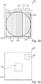
- the semiconductor radiation detector includes a spherical-like detector element in a cube-like detector.
- the detector element is, for example, n + -doped silicon and is provided as a continuous active volume.
- the detector element 203 is, in this embodiment, substantially circular but may also be, for example, ellipsoidal.
- the detector 200 is cube-shaped and includes p-doped bulk silicon semiconductor base material regions 202 in the corners.
- Contact means 214 is arranged for connection to external equipment including contact pins made of aluminum may be provided on the detector.
- a first contact pin 205 may be arranged close to a semiconductor base material region 202 in one of the corners of the detector 200 in contact with the detector element 203 and a second contact pin 206 may be arranged in contact with the spherically shaped active region of the detector 200.
- an outer radiation transparent protection layer 217 made of silicon-oxide (SiO 2 ) may be provided on the detector element.
- the continuous active volume may have a cube-like shape, an ellipsoidal shape, a cylindrical shape, a spherical shape, or a pyramid-like shape. However, other geometrical shapes are conceivable.
Landscapes
- Health & Medical Sciences (AREA)
- Physics & Mathematics (AREA)
- Life Sciences & Earth Sciences (AREA)
- General Physics & Mathematics (AREA)
- High Energy & Nuclear Physics (AREA)
- Molecular Biology (AREA)
- Spectroscopy & Molecular Physics (AREA)
- Measurement Of Radiation (AREA)
- Toxicology (AREA)
Claims (8)
- Halbleiterstrahlungsdetektor, umfassend ein Detektorelement (13), das angeordnet ist, Strahlung in mindestens zwei nicht parallelen Richtungen zu empfangen und eine der empfangenen Strahlung entsprechende Ausgabe zu erzeugen, wobei der Detektor (10) ein dreidimensionales Halbleiterbasismaterial umfasst (12), wobei das Detektorelement so angeordnet ist, dass es einen kontinuierlichen strahlungsempfindlichen pn-Übergang mit dem Halbleiterbasismaterial bildet, wobei das Detektorelement auf allen Seiten des Halbleiterbasismaterials vorgesehen ist, und wobei der Detektor ferner einen ersten Kontakt (15) in Kontakt mit einem Halbleiterbasismaterialbereich und einen zweiten Kontakt (16) in Kontakt mit dem Detektorelement umfasst.
- Halbleiterstrahlungsdetektor nach Anspruch 1, wobei das Detektorelement (13) so angeordnet ist, dass es in mindestens zwei senkrechten Richtungen orientierte Oberflächen aufweist.
- Halbleiterstrahlungsdetektor nach einem der vorhergehenden Ansprüche, wobei das Detektorelement (13) so angeordnet ist, dass es in drei senkrechten Richtungen orientiert Oberflächen aufweist.
- Halbleiterstrahlungsdetektor nach einem der vorhergehenden Ansprüche, wobei das Halbleiterbasismaterial (12) eine polyedrische Form hat.
- Halbleiterstrahlungsdetektor nach einem der vorhergehenden Ansprüche, wobei das Halbleiterbasismaterial (12) würfelförmig ist.
- Halbleiterstrahlungsdetektor nach einem der Ansprüche 1 bis 4, wobei das Halbleiterbasismaterial (12) eine kugelförmige Form hat.
- Halbleiterstrahlungsdetektor nach einem der Ansprüche 1 bis 4, wobei das Halbleiterbasismaterial (12) eine rhomboedrische Form hat.
- Halbleiterstrahlungsdetektor nach einem der vorhergehenden Ansprüche 5 bis 7, wobei der pn-Übergang auf allen Seiten des polyedrischen Halbleiterbasismaterials (12) gebildet ist.
Applications Claiming Priority (1)
| Application Number | Priority Date | Filing Date | Title |
|---|---|---|---|
| PCT/EP2011/058264 WO2012159648A1 (en) | 2011-05-20 | 2011-05-20 | Detector diode |
Publications (2)
| Publication Number | Publication Date |
|---|---|
| EP2710403A1 EP2710403A1 (de) | 2014-03-26 |
| EP2710403B1 true EP2710403B1 (de) | 2020-02-19 |
Family
ID=44119169
Family Applications (1)
| Application Number | Title | Priority Date | Filing Date |
|---|---|---|---|
| EP11722043.4A Active EP2710403B1 (de) | 2011-05-20 | 2011-05-20 | Detektordiode |
Country Status (4)
| Country | Link |
|---|---|
| US (1) | US9778373B2 (de) |
| EP (1) | EP2710403B1 (de) |
| CN (1) | CN103703390A (de) |
| WO (1) | WO2012159648A1 (de) |
Families Citing this family (2)
| Publication number | Priority date | Publication date | Assignee | Title |
|---|---|---|---|---|
| CN108428329B (zh) * | 2018-02-02 | 2023-05-12 | 江苏艾科半导体有限公司 | 一种集成电路ic的封装托盘便携式检测报警装置 |
| EP3909234A4 (de) * | 2019-01-10 | 2022-06-15 | Shenzhen Xpectvision Technology Co., Ltd. | Bildsensor mit strahlungsdetektoren unterschiedlicher ausrichtung |
Family Cites Families (18)
| Publication number | Priority date | Publication date | Assignee | Title |
|---|---|---|---|---|
| US3427454A (en) * | 1965-12-23 | 1969-02-11 | Webb James E | Biomedical radiation detecting probe |
| JPS5536953B2 (de) * | 1974-11-30 | 1980-09-25 | ||
| US4214253A (en) * | 1977-06-13 | 1980-07-22 | General Electric Company | Radiation detector |
| US4207518A (en) * | 1978-03-06 | 1980-06-10 | General Microwave Corporation | Broadband radiation detector with diode elements |
| DE3941706C1 (de) * | 1989-12-18 | 1991-02-28 | Gesellschaft Fuer Strahlen- Und Umweltforschung Mbh, 8042 Neuherberg, De | |
| IL96623A0 (en) * | 1989-12-26 | 1991-09-16 | Gen Electric | Low capacitance,large area semiconductor photodetector and photodetector system |
| US6046454A (en) * | 1995-10-13 | 2000-04-04 | Digirad Corporation | Semiconductor radiation detector with enhanced charge collection |
| US6037595A (en) | 1995-10-13 | 2000-03-14 | Digirad Corporation | Radiation detector with shielding electrode |
| US5698857A (en) * | 1995-12-19 | 1997-12-16 | Eastman Kodak Company | (Barium hafnate: Cu) phosphors and phosphor screens |
| US6614025B2 (en) * | 2000-03-28 | 2003-09-02 | Thomson & Nielsen Electronics Ltd. | Radiation sensor and dosimeter incorporating same |
| JP3900992B2 (ja) * | 2002-04-02 | 2007-04-04 | 株式会社日立製作所 | 放射線検出器及び放射線検査装置 |
| SE0301508D0 (sv) | 2003-05-23 | 2003-05-23 | Goergen Nilsson | Method for pre treatment verification in intensity modulates radiation therapy |
| JP2007127607A (ja) | 2005-11-07 | 2007-05-24 | Mitsutoyo Corp | センサブロック |
| US20120132814A1 (en) * | 2007-02-26 | 2012-05-31 | Irving Weinberg | Radiation detection device, system and related methods |
| EP2130063B1 (de) | 2007-03-09 | 2017-10-18 | European Organisation for Nuclear Research CERN | Verfahren, vorrichtung und computerprogramm zur messung der dosis, dosisrate oder zusammensetzung von strahlung |
| US9557635B2 (en) * | 2007-10-18 | 2017-01-31 | Gearbox, Llc | Ionizing-radiation-responsive compositions, methods, and systems |
| IL189254A0 (en) * | 2008-02-04 | 2008-08-07 | Garber Valery | Quantum uncooled infra-red photo-detector |
| US8039790B2 (en) * | 2009-05-14 | 2011-10-18 | University Health Network | Phantoms and methods for verification in radiotherapy systems |
-
2011
- 2011-05-20 EP EP11722043.4A patent/EP2710403B1/de active Active
- 2011-05-20 WO PCT/EP2011/058264 patent/WO2012159648A1/en not_active Ceased
- 2011-05-20 US US14/118,031 patent/US9778373B2/en active Active
- 2011-05-20 CN CN201180070848.6A patent/CN103703390A/zh active Pending
Non-Patent Citations (1)
| Title |
|---|
| None * |
Also Published As
| Publication number | Publication date |
|---|---|
| WO2012159648A1 (en) | 2012-11-29 |
| CN103703390A (zh) | 2014-04-02 |
| US20140091413A1 (en) | 2014-04-03 |
| US9778373B2 (en) | 2017-10-03 |
| EP2710403A1 (de) | 2014-03-26 |
Similar Documents
| Publication | Publication Date | Title |
|---|---|---|
| Rosenfeld | Novel detectors for silicon based microdosimetry, their concepts and applications | |
| US12019194B2 (en) | Structured detectors and detector systems for radiation imaging | |
| US10712455B2 (en) | Structured detectors and detector systems for radiation imaging | |
| US8421022B2 (en) | Method and apparatus for tissue equivalent solid state microdosimetry | |
| US6528795B2 (en) | Compton scatter imaging instrument | |
| Tran et al. | 3D-Mesa “Bridge” Silicon Microdosimeter: Charge Collection Study and Application to RBE Studies in $^{12}{\rm C} $ Radiation Therapy | |
| US9941440B2 (en) | Radiation microdosimeters correlated with biological cells and cell components | |
| Mackin et al. | The effects of Doppler broadening and detector resolution on the performance of three‐stage Compton cameras | |
| Petasecca et al. | Angular independent silicon detector for dosimetry in external beam radiotherapy | |
| Bläckberg et al. | Light spread manipulation in scintillators using laser induced optical barriers | |
| US9778373B2 (en) | Detector diode | |
| Zahradnik et al. | A diamond guard ring microdosimeter for ion beam therapy | |
| Zhang et al. | Design and performance evaluation of a BGO+ SiPM detector for high-energy prompt gamma imaging in proton therapy monitoring | |
| WO2017017417A1 (en) | Microdosimeter comprising an inductive superconducting transition edge sensor | |
| Domingo-Pardo et al. | A novel γ‐ray imaging method for the pulse-shape characterization of position sensitive semiconductor radiation detectors | |
| Goel et al. | Spatial calibration via imaging techniques of a novel scanning system for the pulse shape characterisation of position sensitive HPGe detectors | |
| Norlin et al. | A cubic isotropic X-ray dose detector diode fabricated by DRIE of SOI substrates | |
| Alhujaili et al. | Characterization of an “edgeless” dosimeter for angular independent measurements in advanced radiotherapy treatments | |
| CN108333620A (zh) | 探测装置及中低能射线源的定位方法 | |
| WO2012138792A1 (en) | Annular-array type beam-position monitor with sub-micron resolution and a parametric method for optimizing photo detectors | |
| Yamaguchi et al. | Imaging of therapeutic carbon-ion beams in a human-head phantom measuring prompt X-rays | |
| Jelinek et al. | Evaluation of Timepix3 with a 1 mm thick silicon sensor as a Compton imaging polarimeter in the hard X-ray band | |
| Granja et al. | Spatial Dosimetry Verification of Conformal Beams in Proton Radiotherapy by Spectral-Sensitive Imaging | |
| US9759672B2 (en) | Radiation detecting wearable devices | |
| McCann et al. | Performance and Inter-Comparison of Novel 4π-Optimized Compton Imagers |
Legal Events
| Date | Code | Title | Description |
|---|---|---|---|
| PUAI | Public reference made under article 153(3) epc to a published international application that has entered the european phase |
Free format text: ORIGINAL CODE: 0009012 |
|
| 17P | Request for examination filed |
Effective date: 20131107 |
|
| AK | Designated contracting states |
Kind code of ref document: A1 Designated state(s): AL AT BE BG CH CY CZ DE DK EE ES FI FR GB GR HR HU IE IS IT LI LT LU LV MC MK MT NL NO PL PT RO RS SE SI SK SM TR |
|
| DAX | Request for extension of the european patent (deleted) | ||
| STAA | Information on the status of an ep patent application or granted ep patent |
Free format text: STATUS: EXAMINATION IS IN PROGRESS |
|
| 17Q | First examination report despatched |
Effective date: 20161220 |
|
| GRAP | Despatch of communication of intention to grant a patent |
Free format text: ORIGINAL CODE: EPIDOSNIGR1 |
|
| STAA | Information on the status of an ep patent application or granted ep patent |
Free format text: STATUS: GRANT OF PATENT IS INTENDED |
|
| INTG | Intention to grant announced |
Effective date: 20190930 |
|
| RIN1 | Information on inventor provided before grant (corrected) |
Inventor name: NILSSON, GOERGEN Inventor name: NORLIN, PETER Inventor name: KAPLAN, WLODEK Inventor name: JUNIQUE, STEPHANE |
|
| GRAS | Grant fee paid |
Free format text: ORIGINAL CODE: EPIDOSNIGR3 |
|
| GRAA | (expected) grant |
Free format text: ORIGINAL CODE: 0009210 |
|
| STAA | Information on the status of an ep patent application or granted ep patent |
Free format text: STATUS: THE PATENT HAS BEEN GRANTED |
|
| AK | Designated contracting states |
Kind code of ref document: B1 Designated state(s): AL AT BE BG CH CY CZ DE DK EE ES FI FR GB GR HR HU IE IS IT LI LT LU LV MC MK MT NL NO PL PT RO RS SE SI SK SM TR |
|
| REG | Reference to a national code |
Ref country code: GB Ref legal event code: FG4D |
|
| REG | Reference to a national code |
Ref country code: CH Ref legal event code: EP |
|
| REG | Reference to a national code |
Ref country code: DE Ref legal event code: R096 Ref document number: 602011065080 Country of ref document: DE |
|
| REG | Reference to a national code |
Ref country code: AT Ref legal event code: REF Ref document number: 1235600 Country of ref document: AT Kind code of ref document: T Effective date: 20200315 |
|
| REG | Reference to a national code |
Ref country code: IE Ref legal event code: FG4D |
|
| REG | Reference to a national code |
Ref country code: NL Ref legal event code: MP Effective date: 20200219 |
|
| PG25 | Lapsed in a contracting state [announced via postgrant information from national office to epo] |
Ref country code: RS Free format text: LAPSE BECAUSE OF FAILURE TO SUBMIT A TRANSLATION OF THE DESCRIPTION OR TO PAY THE FEE WITHIN THE PRESCRIBED TIME-LIMIT Effective date: 20200219 Ref country code: FI Free format text: LAPSE BECAUSE OF FAILURE TO SUBMIT A TRANSLATION OF THE DESCRIPTION OR TO PAY THE FEE WITHIN THE PRESCRIBED TIME-LIMIT Effective date: 20200219 Ref country code: NO Free format text: LAPSE BECAUSE OF FAILURE TO SUBMIT A TRANSLATION OF THE DESCRIPTION OR TO PAY THE FEE WITHIN THE PRESCRIBED TIME-LIMIT Effective date: 20200519 |
|
| REG | Reference to a national code |
Ref country code: LT Ref legal event code: MG4D |
|
| PG25 | Lapsed in a contracting state [announced via postgrant information from national office to epo] |
Ref country code: HR Free format text: LAPSE BECAUSE OF FAILURE TO SUBMIT A TRANSLATION OF THE DESCRIPTION OR TO PAY THE FEE WITHIN THE PRESCRIBED TIME-LIMIT Effective date: 20200219 Ref country code: GR Free format text: LAPSE BECAUSE OF FAILURE TO SUBMIT A TRANSLATION OF THE DESCRIPTION OR TO PAY THE FEE WITHIN THE PRESCRIBED TIME-LIMIT Effective date: 20200520 Ref country code: BG Free format text: LAPSE BECAUSE OF FAILURE TO SUBMIT A TRANSLATION OF THE DESCRIPTION OR TO PAY THE FEE WITHIN THE PRESCRIBED TIME-LIMIT Effective date: 20200519 Ref country code: SE Free format text: LAPSE BECAUSE OF FAILURE TO SUBMIT A TRANSLATION OF THE DESCRIPTION OR TO PAY THE FEE WITHIN THE PRESCRIBED TIME-LIMIT Effective date: 20200219 Ref country code: LV Free format text: LAPSE BECAUSE OF FAILURE TO SUBMIT A TRANSLATION OF THE DESCRIPTION OR TO PAY THE FEE WITHIN THE PRESCRIBED TIME-LIMIT Effective date: 20200219 Ref country code: IS Free format text: LAPSE BECAUSE OF FAILURE TO SUBMIT A TRANSLATION OF THE DESCRIPTION OR TO PAY THE FEE WITHIN THE PRESCRIBED TIME-LIMIT Effective date: 20200619 |
|
| PG25 | Lapsed in a contracting state [announced via postgrant information from national office to epo] |
Ref country code: NL Free format text: LAPSE BECAUSE OF FAILURE TO SUBMIT A TRANSLATION OF THE DESCRIPTION OR TO PAY THE FEE WITHIN THE PRESCRIBED TIME-LIMIT Effective date: 20200219 |
|
| PG25 | Lapsed in a contracting state [announced via postgrant information from national office to epo] |
Ref country code: SK Free format text: LAPSE BECAUSE OF FAILURE TO SUBMIT A TRANSLATION OF THE DESCRIPTION OR TO PAY THE FEE WITHIN THE PRESCRIBED TIME-LIMIT Effective date: 20200219 Ref country code: PT Free format text: LAPSE BECAUSE OF FAILURE TO SUBMIT A TRANSLATION OF THE DESCRIPTION OR TO PAY THE FEE WITHIN THE PRESCRIBED TIME-LIMIT Effective date: 20200712 Ref country code: CZ Free format text: LAPSE BECAUSE OF FAILURE TO SUBMIT A TRANSLATION OF THE DESCRIPTION OR TO PAY THE FEE WITHIN THE PRESCRIBED TIME-LIMIT Effective date: 20200219 Ref country code: RO Free format text: LAPSE BECAUSE OF FAILURE TO SUBMIT A TRANSLATION OF THE DESCRIPTION OR TO PAY THE FEE WITHIN THE PRESCRIBED TIME-LIMIT Effective date: 20200219 Ref country code: SM Free format text: LAPSE BECAUSE OF FAILURE TO SUBMIT A TRANSLATION OF THE DESCRIPTION OR TO PAY THE FEE WITHIN THE PRESCRIBED TIME-LIMIT Effective date: 20200219 Ref country code: EE Free format text: LAPSE BECAUSE OF FAILURE TO SUBMIT A TRANSLATION OF THE DESCRIPTION OR TO PAY THE FEE WITHIN THE PRESCRIBED TIME-LIMIT Effective date: 20200219 Ref country code: DK Free format text: LAPSE BECAUSE OF FAILURE TO SUBMIT A TRANSLATION OF THE DESCRIPTION OR TO PAY THE FEE WITHIN THE PRESCRIBED TIME-LIMIT Effective date: 20200219 Ref country code: ES Free format text: LAPSE BECAUSE OF FAILURE TO SUBMIT A TRANSLATION OF THE DESCRIPTION OR TO PAY THE FEE WITHIN THE PRESCRIBED TIME-LIMIT Effective date: 20200219 Ref country code: LT Free format text: LAPSE BECAUSE OF FAILURE TO SUBMIT A TRANSLATION OF THE DESCRIPTION OR TO PAY THE FEE WITHIN THE PRESCRIBED TIME-LIMIT Effective date: 20200219 |
|
| REG | Reference to a national code |
Ref country code: AT Ref legal event code: MK05 Ref document number: 1235600 Country of ref document: AT Kind code of ref document: T Effective date: 20200219 |
|
| REG | Reference to a national code |
Ref country code: DE Ref legal event code: R097 Ref document number: 602011065080 Country of ref document: DE |
|
| PLBE | No opposition filed within time limit |
Free format text: ORIGINAL CODE: 0009261 |
|
| STAA | Information on the status of an ep patent application or granted ep patent |
Free format text: STATUS: NO OPPOSITION FILED WITHIN TIME LIMIT |
|
| 26N | No opposition filed |
Effective date: 20201120 |
|
| PG25 | Lapsed in a contracting state [announced via postgrant information from national office to epo] |
Ref country code: CH Free format text: LAPSE BECAUSE OF NON-PAYMENT OF DUE FEES Effective date: 20200531 Ref country code: AT Free format text: LAPSE BECAUSE OF FAILURE TO SUBMIT A TRANSLATION OF THE DESCRIPTION OR TO PAY THE FEE WITHIN THE PRESCRIBED TIME-LIMIT Effective date: 20200219 Ref country code: IT Free format text: LAPSE BECAUSE OF FAILURE TO SUBMIT A TRANSLATION OF THE DESCRIPTION OR TO PAY THE FEE WITHIN THE PRESCRIBED TIME-LIMIT Effective date: 20200219 Ref country code: LI Free format text: LAPSE BECAUSE OF NON-PAYMENT OF DUE FEES Effective date: 20200531 Ref country code: MC Free format text: LAPSE BECAUSE OF FAILURE TO SUBMIT A TRANSLATION OF THE DESCRIPTION OR TO PAY THE FEE WITHIN THE PRESCRIBED TIME-LIMIT Effective date: 20200219 |
|
| PG25 | Lapsed in a contracting state [announced via postgrant information from national office to epo] |
Ref country code: PL Free format text: LAPSE BECAUSE OF FAILURE TO SUBMIT A TRANSLATION OF THE DESCRIPTION OR TO PAY THE FEE WITHIN THE PRESCRIBED TIME-LIMIT Effective date: 20200219 Ref country code: SI Free format text: LAPSE BECAUSE OF FAILURE TO SUBMIT A TRANSLATION OF THE DESCRIPTION OR TO PAY THE FEE WITHIN THE PRESCRIBED TIME-LIMIT Effective date: 20200219 |
|
| REG | Reference to a national code |
Ref country code: BE Ref legal event code: MM Effective date: 20200531 |
|
| PG25 | Lapsed in a contracting state [announced via postgrant information from national office to epo] |
Ref country code: LU Free format text: LAPSE BECAUSE OF NON-PAYMENT OF DUE FEES Effective date: 20200520 |
|
| PG25 | Lapsed in a contracting state [announced via postgrant information from national office to epo] |
Ref country code: IE Free format text: LAPSE BECAUSE OF NON-PAYMENT OF DUE FEES Effective date: 20200520 |
|
| PG25 | Lapsed in a contracting state [announced via postgrant information from national office to epo] |
Ref country code: BE Free format text: LAPSE BECAUSE OF NON-PAYMENT OF DUE FEES Effective date: 20200531 |
|
| PG25 | Lapsed in a contracting state [announced via postgrant information from national office to epo] |
Ref country code: TR Free format text: LAPSE BECAUSE OF FAILURE TO SUBMIT A TRANSLATION OF THE DESCRIPTION OR TO PAY THE FEE WITHIN THE PRESCRIBED TIME-LIMIT Effective date: 20200219 Ref country code: MT Free format text: LAPSE BECAUSE OF FAILURE TO SUBMIT A TRANSLATION OF THE DESCRIPTION OR TO PAY THE FEE WITHIN THE PRESCRIBED TIME-LIMIT Effective date: 20200219 Ref country code: CY Free format text: LAPSE BECAUSE OF FAILURE TO SUBMIT A TRANSLATION OF THE DESCRIPTION OR TO PAY THE FEE WITHIN THE PRESCRIBED TIME-LIMIT Effective date: 20200219 |
|
| PG25 | Lapsed in a contracting state [announced via postgrant information from national office to epo] |
Ref country code: MK Free format text: LAPSE BECAUSE OF FAILURE TO SUBMIT A TRANSLATION OF THE DESCRIPTION OR TO PAY THE FEE WITHIN THE PRESCRIBED TIME-LIMIT Effective date: 20200219 Ref country code: AL Free format text: LAPSE BECAUSE OF FAILURE TO SUBMIT A TRANSLATION OF THE DESCRIPTION OR TO PAY THE FEE WITHIN THE PRESCRIBED TIME-LIMIT Effective date: 20200219 |
|
| PGFP | Annual fee paid to national office [announced via postgrant information from national office to epo] |
Ref country code: FR Payment date: 20240614 Year of fee payment: 14 |
|
| PGFP | Annual fee paid to national office [announced via postgrant information from national office to epo] |
Ref country code: GB Payment date: 20250918 Year of fee payment: 15 |
|
| PGFP | Annual fee paid to national office [announced via postgrant information from national office to epo] |
Ref country code: DE Payment date: 20251016 Year of fee payment: 15 |
|
| PG25 | Lapsed in a contracting state [announced via postgrant information from national office to epo] |
Ref country code: FR Free format text: LAPSE BECAUSE OF NON-PAYMENT OF DUE FEES Effective date: 20250531 |