EP2711986B1 - Dispositif à semiconducteur et procédé de fabrication d'un dispositif à semiconducteur - Google Patents
Dispositif à semiconducteur et procédé de fabrication d'un dispositif à semiconducteur Download PDFInfo
- Publication number
- EP2711986B1 EP2711986B1 EP12785949.4A EP12785949A EP2711986B1 EP 2711986 B1 EP2711986 B1 EP 2711986B1 EP 12785949 A EP12785949 A EP 12785949A EP 2711986 B1 EP2711986 B1 EP 2711986B1
- Authority
- EP
- European Patent Office
- Prior art keywords
- conductivity type
- layer
- impurity concentration
- type
- semiconductor substrate
- Prior art date
- Legal status (The legal status is an assumption and is not a legal conclusion. Google has not performed a legal analysis and makes no representation as to the accuracy of the status listed.)
- Active
Links
Images



Classifications
-
- H—ELECTRICITY
- H10—SEMICONDUCTOR DEVICES; ELECTRIC SOLID-STATE DEVICES NOT OTHERWISE PROVIDED FOR
- H10D—INORGANIC ELECTRIC SEMICONDUCTOR DEVICES
- H10D12/00—Bipolar devices controlled by the field effect, e.g. insulated-gate bipolar transistors [IGBT]
- H10D12/01—Manufacture or treatment
- H10D12/031—Manufacture or treatment of IGBTs
- H10D12/032—Manufacture or treatment of IGBTs of vertical IGBTs
- H10D12/038—Manufacture or treatment of IGBTs of vertical IGBTs having a recessed gate, e.g. trench-gate IGBTs
-
- H—ELECTRICITY
- H10—SEMICONDUCTOR DEVICES; ELECTRIC SOLID-STATE DEVICES NOT OTHERWISE PROVIDED FOR
- H10D—INORGANIC ELECTRIC SEMICONDUCTOR DEVICES
- H10D12/00—Bipolar devices controlled by the field effect, e.g. insulated-gate bipolar transistors [IGBT]
- H10D12/411—Insulated-gate bipolar transistors [IGBT]
- H10D12/441—Vertical IGBTs
-
- H—ELECTRICITY
- H10—SEMICONDUCTOR DEVICES; ELECTRIC SOLID-STATE DEVICES NOT OTHERWISE PROVIDED FOR
- H10D—INORGANIC ELECTRIC SEMICONDUCTOR DEVICES
- H10D12/00—Bipolar devices controlled by the field effect, e.g. insulated-gate bipolar transistors [IGBT]
- H10D12/411—Insulated-gate bipolar transistors [IGBT]
- H10D12/441—Vertical IGBTs
- H10D12/461—Vertical IGBTs having non-planar surfaces, e.g. having trenches, recesses or pillars in the surfaces of the emitter, base or collector regions
- H10D12/481—Vertical IGBTs having non-planar surfaces, e.g. having trenches, recesses or pillars in the surfaces of the emitter, base or collector regions having gate structures on slanted surfaces, on vertical surfaces, or in grooves, e.g. trench gate IGBTs
-
- H—ELECTRICITY
- H10—SEMICONDUCTOR DEVICES; ELECTRIC SOLID-STATE DEVICES NOT OTHERWISE PROVIDED FOR
- H10D—INORGANIC ELECTRIC SEMICONDUCTOR DEVICES
- H10D62/00—Semiconductor bodies, or regions thereof, of devices having potential barriers
- H10D62/10—Shapes, relative sizes or dispositions of the regions of the semiconductor bodies; Shapes of the semiconductor bodies
- H10D62/102—Constructional design considerations for preventing surface leakage or controlling electric field concentration
- H10D62/103—Constructional design considerations for preventing surface leakage or controlling electric field concentration for increasing or controlling the breakdown voltage of reverse-biased devices
- H10D62/105—Constructional design considerations for preventing surface leakage or controlling electric field concentration for increasing or controlling the breakdown voltage of reverse-biased devices by having particular doping profiles, shapes or arrangements of PN junctions; by having supplementary regions, e.g. junction termination extension [JTE]
-
- H—ELECTRICITY
- H10—SEMICONDUCTOR DEVICES; ELECTRIC SOLID-STATE DEVICES NOT OTHERWISE PROVIDED FOR
- H10D—INORGANIC ELECTRIC SEMICONDUCTOR DEVICES
- H10D62/00—Semiconductor bodies, or regions thereof, of devices having potential barriers
- H10D62/10—Shapes, relative sizes or dispositions of the regions of the semiconductor bodies; Shapes of the semiconductor bodies
- H10D62/102—Constructional design considerations for preventing surface leakage or controlling electric field concentration
- H10D62/103—Constructional design considerations for preventing surface leakage or controlling electric field concentration for increasing or controlling the breakdown voltage of reverse-biased devices
- H10D62/105—Constructional design considerations for preventing surface leakage or controlling electric field concentration for increasing or controlling the breakdown voltage of reverse-biased devices by having particular doping profiles, shapes or arrangements of PN junctions; by having supplementary regions, e.g. junction termination extension [JTE]
- H10D62/106—Constructional design considerations for preventing surface leakage or controlling electric field concentration for increasing or controlling the breakdown voltage of reverse-biased devices by having particular doping profiles, shapes or arrangements of PN junctions; by having supplementary regions, e.g. junction termination extension [JTE] having supplementary regions doped oppositely to or in rectifying contact with regions of the semiconductor bodies, e.g. guard rings with PN or Schottky junctions
-
- H—ELECTRICITY
- H10—SEMICONDUCTOR DEVICES; ELECTRIC SOLID-STATE DEVICES NOT OTHERWISE PROVIDED FOR
- H10D—INORGANIC ELECTRIC SEMICONDUCTOR DEVICES
- H10D62/00—Semiconductor bodies, or regions thereof, of devices having potential barriers
- H10D62/10—Shapes, relative sizes or dispositions of the regions of the semiconductor bodies; Shapes of the semiconductor bodies
- H10D62/13—Semiconductor regions connected to electrodes carrying current to be rectified, amplified or switched, e.g. source or drain regions
- H10D62/133—Emitter regions of BJTs
-
- H—ELECTRICITY
- H10—SEMICONDUCTOR DEVICES; ELECTRIC SOLID-STATE DEVICES NOT OTHERWISE PROVIDED FOR
- H10D—INORGANIC ELECTRIC SEMICONDUCTOR DEVICES
- H10D62/00—Semiconductor bodies, or regions thereof, of devices having potential barriers
- H10D62/10—Shapes, relative sizes or dispositions of the regions of the semiconductor bodies; Shapes of the semiconductor bodies
- H10D62/13—Semiconductor regions connected to electrodes carrying current to be rectified, amplified or switched, e.g. source or drain regions
- H10D62/137—Collector regions of BJTs
-
- H—ELECTRICITY
- H10—SEMICONDUCTOR DEVICES; ELECTRIC SOLID-STATE DEVICES NOT OTHERWISE PROVIDED FOR
- H10D—INORGANIC ELECTRIC SEMICONDUCTOR DEVICES
- H10D62/00—Semiconductor bodies, or regions thereof, of devices having potential barriers
- H10D62/10—Shapes, relative sizes or dispositions of the regions of the semiconductor bodies; Shapes of the semiconductor bodies
- H10D62/13—Semiconductor regions connected to electrodes carrying current to be rectified, amplified or switched, e.g. source or drain regions
- H10D62/141—Anode or cathode regions of thyristors; Collector or emitter regions of gated bipolar-mode devices, e.g. of IGBTs
- H10D62/142—Anode regions of thyristors or collector regions of gated bipolar-mode devices
-
- H—ELECTRICITY
- H10—SEMICONDUCTOR DEVICES; ELECTRIC SOLID-STATE DEVICES NOT OTHERWISE PROVIDED FOR
- H10D—INORGANIC ELECTRIC SEMICONDUCTOR DEVICES
- H10D62/00—Semiconductor bodies, or regions thereof, of devices having potential barriers
- H10D62/10—Shapes, relative sizes or dispositions of the regions of the semiconductor bodies; Shapes of the semiconductor bodies
- H10D62/17—Semiconductor regions connected to electrodes not carrying current to be rectified, amplified or switched, e.g. channel regions
- H10D62/177—Base regions of bipolar transistors, e.g. BJTs or IGBTs
-
- H—ELECTRICITY
- H10—SEMICONDUCTOR DEVICES; ELECTRIC SOLID-STATE DEVICES NOT OTHERWISE PROVIDED FOR
- H10D—INORGANIC ELECTRIC SEMICONDUCTOR DEVICES
- H10D62/00—Semiconductor bodies, or regions thereof, of devices having potential barriers
- H10D62/10—Shapes, relative sizes or dispositions of the regions of the semiconductor bodies; Shapes of the semiconductor bodies
- H10D62/17—Semiconductor regions connected to electrodes not carrying current to be rectified, amplified or switched, e.g. channel regions
- H10D62/393—Body regions of DMOS transistors or IGBTs
-
- H—ELECTRICITY
- H10—SEMICONDUCTOR DEVICES; ELECTRIC SOLID-STATE DEVICES NOT OTHERWISE PROVIDED FOR
- H10D—INORGANIC ELECTRIC SEMICONDUCTOR DEVICES
- H10D62/00—Semiconductor bodies, or regions thereof, of devices having potential barriers
- H10D62/60—Impurity distributions or concentrations
-
- H—ELECTRICITY
- H10—SEMICONDUCTOR DEVICES; ELECTRIC SOLID-STATE DEVICES NOT OTHERWISE PROVIDED FOR
- H10D—INORGANIC ELECTRIC SEMICONDUCTOR DEVICES
- H10D62/00—Semiconductor bodies, or regions thereof, of devices having potential barriers
- H10D62/80—Semiconductor bodies, or regions thereof, of devices having potential barriers characterised by the materials
- H10D62/83—Semiconductor bodies, or regions thereof, of devices having potential barriers characterised by the materials being Group IV materials, e.g. B-doped Si or undoped Ge
- H10D62/834—Semiconductor bodies, or regions thereof, of devices having potential barriers characterised by the materials being Group IV materials, e.g. B-doped Si or undoped Ge further characterised by the dopants
-
- H—ELECTRICITY
- H10—SEMICONDUCTOR DEVICES; ELECTRIC SOLID-STATE DEVICES NOT OTHERWISE PROVIDED FOR
- H10D—INORGANIC ELECTRIC SEMICONDUCTOR DEVICES
- H10D64/00—Electrodes of devices having potential barriers
- H10D64/20—Electrodes characterised by their shapes, relative sizes or dispositions
- H10D64/27—Electrodes not carrying the current to be rectified, amplified, oscillated or switched, e.g. gates
- H10D64/311—Gate electrodes for field-effect devices
- H10D64/411—Gate electrodes for field-effect devices for FETs
- H10D64/511—Gate electrodes for field-effect devices for FETs for IGFETs
- H10D64/512—Disposition of the gate electrodes, e.g. buried gates
- H10D64/513—Disposition of the gate electrodes, e.g. buried gates within recesses in the substrate, e.g. trench gates, groove gates or buried gates
-
- H—ELECTRICITY
- H10—SEMICONDUCTOR DEVICES; ELECTRIC SOLID-STATE DEVICES NOT OTHERWISE PROVIDED FOR
- H10P—GENERIC PROCESSES OR APPARATUS FOR THE MANUFACTURE OR TREATMENT OF DEVICES COVERED BY CLASS H10
- H10P14/00—Formation of materials, e.g. in the shape of layers or pillars
- H10P14/40—Formation of materials, e.g. in the shape of layers or pillars of conductive or resistive materials
- H10P14/42—Formation of materials, e.g. in the shape of layers or pillars of conductive or resistive materials using a gas or vapour
- H10P14/44—Physical vapour deposition [PVD]
-
- H—ELECTRICITY
- H10—SEMICONDUCTOR DEVICES; ELECTRIC SOLID-STATE DEVICES NOT OTHERWISE PROVIDED FOR
- H10P—GENERIC PROCESSES OR APPARATUS FOR THE MANUFACTURE OR TREATMENT OF DEVICES COVERED BY CLASS H10
- H10P30/00—Ion implantation into wafers, substrates or parts of devices
- H10P30/20—Ion implantation into wafers, substrates or parts of devices into semiconductor materials, e.g. for doping
- H10P30/202—Ion implantation into wafers, substrates or parts of devices into semiconductor materials, e.g. for doping characterised by the semiconductor materials
- H10P30/204—Ion implantation into wafers, substrates or parts of devices into semiconductor materials, e.g. for doping characterised by the semiconductor materials into Group IV semiconductors
-
- H—ELECTRICITY
- H10—SEMICONDUCTOR DEVICES; ELECTRIC SOLID-STATE DEVICES NOT OTHERWISE PROVIDED FOR
- H10P—GENERIC PROCESSES OR APPARATUS FOR THE MANUFACTURE OR TREATMENT OF DEVICES COVERED BY CLASS H10
- H10P30/00—Ion implantation into wafers, substrates or parts of devices
- H10P30/20—Ion implantation into wafers, substrates or parts of devices into semiconductor materials, e.g. for doping
- H10P30/21—Ion implantation into wafers, substrates or parts of devices into semiconductor materials, e.g. for doping of electrically active species
-
- H—ELECTRICITY
- H10—SEMICONDUCTOR DEVICES; ELECTRIC SOLID-STATE DEVICES NOT OTHERWISE PROVIDED FOR
- H10P—GENERIC PROCESSES OR APPARATUS FOR THE MANUFACTURE OR TREATMENT OF DEVICES COVERED BY CLASS H10
- H10P95/00—Generic processes or apparatus for manufacture or treatments not covered by the other groups of this subclass
- H10P95/90—Thermal treatments, e.g. annealing or sintering
-
- H—ELECTRICITY
- H10—SEMICONDUCTOR DEVICES; ELECTRIC SOLID-STATE DEVICES NOT OTHERWISE PROVIDED FOR
- H10D—INORGANIC ELECTRIC SEMICONDUCTOR DEVICES
- H10D62/00—Semiconductor bodies, or regions thereof, of devices having potential barriers
- H10D62/10—Shapes, relative sizes or dispositions of the regions of the semiconductor bodies; Shapes of the semiconductor bodies
- H10D62/13—Semiconductor regions connected to electrodes carrying current to be rectified, amplified or switched, e.g. source or drain regions
- H10D62/149—Source or drain regions of field-effect devices
- H10D62/151—Source or drain regions of field-effect devices of IGFETs
Definitions
- the present invention relates to a semiconductor device and semiconductor device manufacturing method such that a field-stop layer is provided on a substrate back surface side.
- IGBT Insulated Gate Bipolar Transistor
- MOSFET Metal-Oxide-Semiconductor Field Effect Transistor
- IGBTs are also often used together with an FWD (free wheeling diode) or the like, and have expanded to be used in the field of industrial instruments such as general purpose and electric vehicle inverters and alternating current (AC) servos, uninterruptible power supplies (UPS), and switching power supplies, and in the field of consumer instruments such as microwave cookers, rice cookers, and stroboscopes.
- FWD free wheeling diode
- IGBTs with lower on-state voltages have been developed as elements improved to next generation types, and lower loss and higher efficiency have been achieved for applied devices.
- a field-stop (FS) IGBT (hereafter referred to as a trench-FS-IGBT) including a trench MOS gate (an insulated gate formed of a metal-oxide film-semiconductor) structure (hereafter referred to as a trench MOS structure) is commonly known as an IGBT.
- Fig. 5 is a main portion sectional view showing the configuration of a heretofore known FS-IGBT.
- the trench-FS-IGBT includes a plurality of trenches 11 on the front surface side of a Si substrate that forms an n - type drift layer 1.
- a gate dielectric film 10 is provided along the inner wall of the trench 11, and a gate electrode 7 is provided on the inner side of the gate dielectric film 10.
- a p-type base layer 5 is provided in portions of the Si substrate sandwiched between the trenches 11, whereby a trench MOS structure 12 formed of the gate electrode 7, gate dielectric film 10, and p-type base layer 5 is configured on the front surface side of the Si substrate.
- an n + type emitter region 4 and p + contact region 6 are selectively provided in a surface layer of the p-type base layer 5.
- the n + type emitter region 4 is disposed so as to be in contact with the upper side (aperture portion side) end of a side surface of the trench 11.
- An emitter electrode 9 is provided forming ohmic contact to both the n + type emitter region 4 and p-type base layer 5 (p + contact region 6) .
- a p + type collector layer 3 and a collector electrode 8 are provided on the back surface side of the Si substrate.
- a field-stop (FS) layer 2 is provided between the p + type collector layer 3 and n - type drift layer 1.
- the FZ-n-type Si substrate that forms the n - type drift layer 1 it is possible to reduce the wafer cost. Also, by providing the FS layer 2, it is possible for the thickness of the Si substrate to be less than that of a non-punch through (NP) IGBT, and to be a thickness commensurate with the breakdown voltage, and thus possible to reduce the on-state voltage. Also, by the p + type collector layer 3 being a low implantation collector that has a low dose and is shallow, it is possible to turn off at a high speed without carrying out lifetime control using electronic irradiation or the like.
- NP non-punch through
- the trench-FS-IGBT shown in Fig. 5 is such that, by the FS layer 2 being provided, it is possible to reduce the on-state voltage by reducing the thickness of the Si substrate (wafer) .
- a thin wafer is liable to crack during the manufacturing process, causing the efficiency rate to deteriorate, because of which a wafer that has not been thinned is used as it is when being introduced into the manufacturing process.
- the wafer is thinned to a thickness necessary for the breakdown voltage.
- a back grinding process whereby the wafer is thinned from the back surface by grinding, etching, or the like, has been proposed as a process for thinning the wafer (for example, refer to PTL 1).
- a method whereby a two-stage buffer layer (FS layer), configured of a diffusion layer with a low impurity concentration formed deeply from the wafer back surface side and a diffusion layer with a high impurity concentration formed shallowly from the wafer back surface side, is formed using phosphorus (P) as the dopant for forming the FS layer or buffer layer (not shown) has been proposed as a method of improving the voltage resistance of the FS-IGBT (for example, refer to PTL 2) .
- PTL 2 by adopting a two-stage buffer layer, it is possible to prevent the occurrence of drain voltage and drain current oscillation, which is liable to occur when turning off. Also, it is possible to prevent an adverse effect on characteristics depending on the precision of the amount of polishing when back grinding in order to thin the wafer.
- a method whereby the FS-layer is efficiently formed as a deep diffusion layer with a low impurity concentration using an n-type impurity such as selenium (Se) or sulfur (S), which have a higher diffusion constant than that of phosphorus, rather than phosphorus as the dopant for forming the FS layer has been proposed as a method of forming an FS-IGBT (for example, refer to PTL 3).
- an FS-IGBT including a structure wherein the ratio between the widths of the drift layer and depletion layer and the ratio between the impurity concentrations of the collector layer and buffer layer are each regulated has been proposed as a high breakdown voltage FS-IGBT wherein the voltage resistance in a safe operation region at a time of a short circuit current shut-off is improved (for example, refer to PTL 4).
- US 2009/184340 A1 describes a semiconductor device in which a semiconductor substrate can be prevented from being broken while elements can be prevented from being destroyed by a snap-back phenomenon. After an MOS gate structure is formed in a front surface of an FZ wafer, a rear surface of the FZ wafer is ground.
- the ground surface is irradiated with protons and irradiated with two kinds of laser beams different in wavelength simultaneously to thereby form an N+ first buffer layer and an N second buffer layer.
- a P+ collector layer and a collector electrode are formed on the proton-irradiated surface.
- the distance from a position where the net doping concentration of the N+ first buffer layer is locally maximized to the interface between the P+ collector layer and the N second buffer layer is set to be in a range of 5 mum to 30 mum, both inclusively.
- JP 2002 314084 A describes a method of manufacturing a semiconductor device. After an emitter electrode is formed, a principal surface on an opposite side is polished to a predetermined thickness to make a center line average roughness of a polished surface 1 mum or less and a filtered wave at the center line 10 mum or less. Only the polished surface is selectively cleaned with a chemical to remove particles and then, in order to form a field stop layer, phosphorus ions are implanted into the cleaned surface by an ion implanting method, and then, in order to form a collector layer, boron irons are implanted by the ion implanting method.
- the wafer is put in a diffusion furnace and is subjected to heat treatment at a temperature from 300 deg.C to 550 deg.C to form the field stop layer and the collector, and then a collector electrode is formed.
- a portion contacting the semiconductor of the collector electrode is made of aluminum or platinum 0.3 mum or thicker.
- JP 2008 211148 A describes a semiconductor device having an MOS gate structure comprising an N drift layer, a field stop layer, a P collector layer, a collector electrode, a P base layer, an N emitter region, a gate insulating film, and a gate electrode, and an emitter electrode.
- a Frenkel defect of higher than heat balancing density is introduced in the N drift layer and the sum of the lifetime of electrons and the lifetime of holes in the N drift layer is 0.1 to 60 mus. Further, the sum of the depth-directional thickness of the N drift layer and the depth-directional thickness of the field stop layer is smaller than the diffusion length of electrons and holes when the Frenkel defect density of the N drift layer is the heat balancing density.
- WO 2011/052787 A1 describes a semiconductor device wherein a p anode layer is formed on the side of one main surface of an n- drift layer. On the side of the other main surface of the n- drift layer, an n+ cathode layer having an impurity concentration higher than that of the n- drift layer is formed. On the surface of the p anode layer, an anode electrode is formed. On the surface of the n+ cathode layer, a cathode electrode is formed.
- An n type broad buffer region is formed inside of the n- drift layer, said broad buffer region having a net doping concentration higher than that of the bulk of a wafer and lower than that of the n+ cathode layer and that of the p anode layer.
- the invention in order to eliminate the heretofore described problems with the heretofore known technology, has an object of providing a semiconductor device and semiconductor device manufacturing method such that it is possible to balance an improvement in resistance to element destruction when a short circuit occurs with suppressing thermal runaway destruction. Also, the invention, in order to eliminate the heretofore described problems with the heretofore known technology, has an object of providing a semiconductor device and semiconductor device manufacturing method such that it is also possible to reduce variation in on-state voltage.
- a semiconductor device as defined in claim 1, includes a first conductivity type drift layer formed of a first conductivity type semiconductor substrate, a second conductivity type base layer formed in a surface layer of one main surface of the first conductivity type semiconductor substrate, a first conductivity type emitter layer formed in a surface layer on the first conductivity type semiconductor substrate one main surface side of the second conductivity type base layer, a gate dielectric film provided on the one main surface of the first conductivity type semiconductor substrate and in contact with the first conductivity type emitter layer, second conductivity type base layer, and first conductivity type drift layer, a gate electrode facing the first conductivity type emitter layer, second conductivity type base layer, and first conductivity type drift layer with the gate dielectric film interposed therebetween, a MOS gate structure formed of the first conductivity type drift layer
- the semiconductor device according to the first aspect of the invention has the maximum impurity concentration of the second conductivity type collector layer is 6 ⁇ 10 16 cm -3 or more, 1 ⁇ 10 20 cm -3 or less. Also, in the semiconductor device according to the first aspect of the invention the dopant of the first conductivity type field-stop layer is selenium or sulfur.
- the dopant of the first conductivity type buffer layer is phosphorus.
- the maximum impurity concentration of the first conductivity type field-stop layer is 3 ⁇ 10 14 cm -3 or more, 3 ⁇ 10 15 cm -3 or less.
- the concentration gradient of the first conductivity type field-stop layer becomes gradually smaller from the position of the maximum impurity concentration of the first conductivity type field-stop layer toward the one main surface side of the first conductivity type semiconductor substrate. Also, the semiconductor device according to the first aspect of the invention has the rated voltage of 1,200V or higher.
- a semiconductor device manufacturing method as defined in claim 8 is a method of manufacturing a semiconductor device including a first conductivity type drift layer formed of a first conductivity type semiconductor substrate, a MOS gate structure formed of at least a gate electrode, a gate dielectric film, and the first conductivity type semiconductor substrate provided on one main surface side of the first conductivity type semiconductor substrate, a second conductivity type collector layer provided on the other main surface of the first conductivity type semiconductor substrate, a first conductivity type field-stop layer provided between the first conductivity type drift layer and second conductivity type collector layer and having an impurity concentration higher than that of the first conductivity type drift layer, and a first conductivity type buffer layer provided between the first conductivity type field-stop layer and second conductivity type collector layer and having an impurity concentration higher than that of the first conductivity type field-stop layer, and has the following characteristics.
- the MOS gate structure is formed on the one main surface side of the first conductivity type semiconductor substrate (a MOS gate structure formation step).
- the other main surface of the first conductivity type semiconductor substrate is ground to reduce the first conductivity type semiconductor substrate to a predetermined thickness (a substrate thinning step).
- dopants are ion implanted into the ground surface of the first conductivity type semiconductor substrate in order to form each of the first conductivity type field-stop layer, first conductivity type buffer layer, and second conductivity type collector layer (an implantation step).
- heat treatment for simultaneously electrically activating the plurality of dopants ion implanted into the ground surface of the first conductivity type semiconductor substrate is carried out (an activation step).
- a metal electrode film is formed by sputtering on the one main surface of the first conductivity type semiconductor substrate and carrying out heat treatment (an electrode film formation step).
- the implantation step and activation step are carried out so that the net doping concentration of the first conductivity type field-stop layer is higher than the net doping concentration of the first conductivity type drift layer, the total of the net doping concentration of the first conductivity type field-stop layer and net doping concentration of the first conductivity type drift layer has a value such that a depletion layer end of a depletion layer spreading in the first conductivity type drift layer and first conductivity type field-stop layer in response to an application of a rated voltage is inside the first conductivity type field-stop layer, the impurity concentration distribution of the first conductivity type field-stop layer has a concentration gradient that decreases from the other main surface side of the first conductivity type semiconductor substrate toward the one main surface side, the depth of the first conductivity type field-stop layer is 20 ⁇ m or more, and the maximum impurity concentration of the first conductivity type buffer layer is higher than the maximum impurity concentration of the first conductivity type field-stop layer at 6 ⁇ 10 15 cm -3 or more,
- the amount of holes implanted from the collector side when a short circuit occurs increases, and the rise of a magnetic field intensity on the collector side is suppressed, by forming a first conductivity type field-stop layer that is deep and of a low impurity concentration, and that has a gentle concentration gradient, using selenium or sulfur as a dopant. Also, by providing a first conductivity type buffer layer having a predetermined peak impurity concentration between the first conductivity type field-stop layer and a second conductivity type collector layer using an ion implantation of phosphorus, it is possible to suppress an implantation of holes contributing to an increase in leakage current. Also, according to the invention, it is possible to reduce on-state voltage variation by arranging that the peak impurity concentration of the first conductivity type buffer layer is at least one digit lower than the peak impurity concentration of the second conductivity type collector layer.
- an advantage is achieved in that it is possible to balance improving resistance to element destruction by spreading a space-charge region at an early stage when a short circuit occurs with suppressing thermal runaway destruction caused by an implantation of holes. Also, according to the semiconductor device and semiconductor device manufacturing method according to the invention, an advantage is achieved in that it is possible to reduce variation in on-state voltage.
- a layer or region being prefixed by n or p indicates that electrons or holes respectively are majority carriers.
- a description is given with a first conductivity type as an n-type and a second conductivity type as a p-type, but the invention is established in the same way when the first conductivity type is a p-type and the second conductivity type an n-type.
- n or p indicates a higher impurity concentration or lower impurity concentration respectively than that in a layer or region to which neither is added.
- an impurity determining whether a semiconductor is a p-type or an n-type is also called a dopant.
- An impurity concentration indicates a net doping concentration resulting from an electrically activated dopant, unless specifically indicated otherwise.
- FIG. 1 is a main portion sectional view showing the configuration of the FS-IGBT according to the embodiment of the invention.
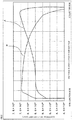
- Fig. 6 is a characteristic diagram showing the impurity concentration distribution of the FS-IGBT according to the embodiment of the invention.
- Fig. 6 shows the impurity concentration distribution from the back surface to an n - type drift layer 1 of a silicon (Si) substrate (semiconductor substrate) configuring the trench-FS-IGBT (the same also applies to Fig. 7 ).
- the trench-FS-IGBT shown in Fig. 1 is configured using, for example, an FZ-n-type Si substrate formed of an inexpensive FZ wafer.
- the resistivity of the Si substrate may be in the region of, for example, 80 ⁇ cm to 130 ⁇ cm.
- the thickness of the finished Si substrate may be in the region of, for example, 160 ⁇ m to 210 ⁇ m.
- the thickness of the finished Si substrate is the thickness of the Si substrate configuring the product after the FS-IGBT is completed.
- the layer structure inside the Si substrate is as follows. A plurality of trenches 11 are provided at predetermined intervals in one main surface (the front surface) of the Si substrate, which forms the n - type drift layer 1.
- a gate dielectric film 10 is provided along the inner wall of the trench 11, and a gate electrode 7 is provided on the inner side of the gate dielectric film 10.
- a p-type base layer 5 is provided in portions of the Si substrate sandwiched between the trenches 11, whereby a trench MOS gate (an insulated gate formed of a metal-oxide film-semiconductor) structure (trench MOS structure) 12 formed of the gate electrode 7, gate dielectric film 10, p-type base layer 5, and the like is configured on the front surface side of the Si substrate.
- An n + type emitter region 4 and p + contact region 6 are selectively provided in a surface layer of each p-type base layer 5 among the plurality of trenches 11.
- the n + type emitter region 4 is disposed so as to be in contact with the upper side (aperture portion side) end of a side surface of the trench 11.
- the p + contact region 6 is disposed so as to be in contact with the n + type emitter region 4.
- An emitter electrode 9 is provided forming an ohmic contact to the surface of the n + type emitter region 4 and the surface of the p-type base layer 5 (or with the p + contact region 6 in the surface layer of the p-type base layer 5) .
- the emitter electrode 9 is electrically insulated from the gate electrode 7 by an interlayer dielectric film.
- a p + type collector layer 15 and a collector electrode 8 forming an ohmic contact to the surface of the p + type collector layer 15 are provided on the back surface (other main surface) side of the Si substrate.
- An n-type layer structure formed of an n + type buffer layer 13 having a peak impurity concentration (maximum impurity concentration of the impurity concentration distribution) peculiar to the invention and an n-type field-stop (FS) layer 14 deep toward the n - type drift layer 1 side via the n + type buffer layer 13 is configured as a characteristic of the invention on the n - type drift layer 1 side of the p + type collector layer 15.
- the impurity concentration distribution of the p + type collector layer 15, n + type buffer layer 13, n-type FS layer 14, and n - type drift layer 1 in the depth direction from the back surface of the Si substrate (or an IGBT chip) is shown in Fig. 6 .
- n-type FS layer 14 It is preferable that, for example, selenium or sulfur, which have a higher diffusion coefficient than that of phosphorus at the same temperature, is used as an ion implantation dopant for forming the n-type FS layer 14, and more preferable that selenium is used.
- the maximum impurity concentration of the n-type FS layer 14 is within a range of 3 ⁇ 10 14 cm -3 to 3 ⁇ 10 15 cm -3 .
- the diffusion depth of the n-type FS layer 14 is such that the interface of the n-type FS layer 14 and n - type drift layer 1 is within a range of 20 ⁇ m or more, 40 ⁇ m or less from the back surface of the Si substrate.
- An ion implantation of, for example, selenium for forming the n-type FS layer 14, and a subsequent thermal diffusion process, are carried out under conditions within these kinds of maximum impurity concentration and diffusion depth ranges.
- the depth from the back surface of the Si substrate to the interface of the n-type FS layer 14 and n - type drift layer 1 may be 30 ⁇ m.
- the impurity concentration distribution from the back surface of the Si substrate to a depth of 30 ⁇ m has a concentration gradient such that an n-type impurity concentration exhibits the highest value (for example, 3 ⁇ 10 15 cm -3 ) in the vicinity of the Si substrate back surface side surface, and the n-type impurity concentration becomes lower the deeper in the depth direction from the Si substrate back surface side.
- the impurity concentration and diffusion depth from the Si substrate back surface of a portion of the n-type FS layer 14 having the maximum impurity concentration are such that the total value of the total impurity of the n-type FS layer 14 and total impurity of the n - type drift layer 1 at least satisfies the following relationship.
- the total value of the total impurity of the n-type FS layer 14 and total impurity of the n - type drift layer 1 in the depletion layer is a value such that a leading end portion of the depletion layer (a depletion layer end) is inside the n-type FS layer 14, that is, a value sufficient that the spread of the depletion layer is stopped inside the n-type FS layer 14.
- the total impurity (or impurity total) is a value wherein the impurity concentration of a certain layer is integrated in a depth direction (a direction headed perpendicularly from the front surface of the semiconductor substrate toward the back surface, or a direction the opposite thereof) .
- the total value of the total impurity of the n-type FS layer 14 and total impurity of the n - type drift layer 1 in the depletion layer is the total value, in the region in which the depletion layer spreads, of a value of the impurity concentration of the n - type drift layer 1 from the position (depth) of the p-n junction between the p-type base layer 5 and n - type drift layer 1 to the position of the interface between the n - type drift layer 1 and n-type FS layer 14 integrated in the depth direction and the value of the impurity concentration of the n-type FS layer 14 from the position in which the n - type drift layer 1 and n-type FS layer 14 intersect to the position of the depletion layer edge integrated in the depth direction.
- the depletion layer end of the depletion layer spreading when the rated voltage is applied does not reach the p + type collector layer 15, and that there is a certain distance (for example, 3 ⁇ m or more) between the p + type collector layer 15 and depletion layer end.
- a certain distance for example, 3 ⁇ m or more
- the n-type FS layer 14 which is deep in the depth direction from the Si substrate back surface and which has a concentration gradient such that the impurity concentration becomes gradually lower from the p + type collector layer 15 side in the depth direction from the back surface, it is possible to alleviate the electrical field intensity attenuation rate of the electrical field intensity distribution of the depletion layer end spreading when the rated voltage is applied. Because of this, the n-type FS layer 14 has functions of suppressing voltage waveform or current waveform oscillation liable to occur when turning off, and reducing voltage waveform or current waveform amplitude.
- the following advantages are obtained by forming a diffusion layer with a depth of 20 ⁇ m or more, which is to become the n-type FS layer 14, using selenium or sulfur as a dopant.
- a dopant When ion implanting a dopant into a semiconductor substrate (wafer), it may happen that particles of in the region of a few micrometers in size existing in the implantation surface form an ion implantation shadow that blocks ions, whereby a defect region into which ions are not implanted is formed inside the semiconductor substrate.
- the dopant diffuses to a depth a few times greater than the size of the particles. Because of this, owing to a lateral diffusion (a diffusion in a direction perpendicular to the substrate depth direction) of the selenium or sulfur, the dopant also diffuses to the region to which ion implantation is blocked by the particles. Consequently, it is possible to reduce ion implantation unevenness occurring because of the particles to an extent such that characteristics such as breakdown voltage and leakage current do not depreciate.
- the invention is of a configuration such that, in addition to the deep n-type FS layer 14 being formed by a selenium ion implantation, the n + buffer layer 13 formed by a phosphorus ion implantation peculiar to the invention is provided between the n-type FS layer 14 and p + collector layer 15.
- the n-type FS layer 14 impurity concentration has a lower overall concentration gradient, as with selenium, in order to prevent element destruction when a short circuit occurs. The reason for this is as follows.
- the impurity concentration of the n-type FS layer 14 is such that the depletion layer end when the rated voltage is applied with the gate in an off-state is inside the n-type FS layer 14, as previously described, the peak impurity concentration of the n-type FS layer 14 in the vicinity of the p + type collector layer 15 also decreases. Because of this, there is a problem in that the injection efficiency of holes from the p + type collector layer 15 increases, the leakage current increases, and the possibility of thermal runaway destruction increases.
- n + buffer layer 13 between the n-type FS layer 14 and p + collector layer 15 using a phosphorus ion implantation, as in the case of the invention, it is possible to suppress an implantation of holes contributing to an increase in leakage current.
- phosphorus it is also possible to use arsenic (As) in the n + buffer layer 13.
- sulfur it is also possible to use sulfur as the n-type impurity forming the n-type FS layer 14, as previously described.
- the n + buffer layer 13 has a thickness of 0.5 ⁇ m to 3.0 ⁇ m, that the peak impurity concentration is at least 6 ⁇ 10 15 cm -3 or more, and that the n + buffer layer 13 is formed by a phosphorus ion implantation so as to have a small peak impurity concentration one-tenth or less that of the peak impurity concentration of the p + collector layer 15.
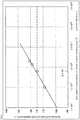
- a description will be given, referring to Fig. 3 , of the reason that it is preferable that the peak impurity concentration of the n + buffer layer 13 is 6 ⁇ 10 15 cm -3 or more.
- the maximum allowable junction temperature is the maximum junction temperature allowed in the p-n junction portion between the n + buffer layer 13 and p + collector layer 15 (hereafter referred to as the maximum allowable junction temperature).
- the n + buffer layer 13 has a function of suppressing the implantation of holes from the p + type collector layer 15.
- the maximum allowable junction temperature is 175°C or higher, as shown in Fig. 3 .
- the maximum guaranteed operating temperature when actually using the element is a temperature guaranteeing that thermal runaway due to leakage current (positive feedback whereby a temperature rise caused by leakage current causes a further increase in leakage current) does not occur at that temperature or lower, and is normally 175°C. Consequently, thermal runaway due to leakage current should not occur at or below the maximum guaranteed operating temperature. From the results shown in Fig. 3 , it is seen that, in order to prevent thermal runaway at 175°C, it is good when the peak impurity concentration of the n + buffer layer 13 is 6 ⁇ 10 15 cm -3 or more.
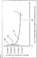
- Fig. 4 is a characteristic diagram showing on-state voltage variation according to the ratio between the peak impurity concentration of the buffer layer of the FS-IGBT according to the invention and the peak impurity concentration of the collector layer.
- the variation in the on-state voltage (Von) can be reduced by arranging that the peak impurity concentration of the n + buffer layer 13 is at least one digit lower than the peak impurity concentration of the p + type collector layer 15. As a result of this, the efficiency rate is improved. It has been confirmed above, from the results shown in Figs. 3 and 4 , that the peak impurity concentration of the n + buffer layer 13 is 6 ⁇ 10 15 cm -3 or more, and is at least one digit lower than the peak impurity concentration of the p + type collector layer 15.
- the maximum impurity concentration (peak impurity concentration) of the p + type collector layer 15 is within a range of 6 ⁇ 101 6 cm -3 or more, 1 ⁇ 10 20 cm -3 or less, and preferably within a range of 6 ⁇ 101 6 cm -3 or more, 1 ⁇ 10 18 cm -3 or less, for example, 1 ⁇ 10 17 cm -3 .
- the p + type collector layer 15 has a function as a low implantation collector with low hole injection efficiency, and needs to be formed with a surface impurity concentration that is a peak impurity concentration ten times or more higher than the peak impurity concentration of the n + buffer layer 13, as heretofore described, and that forms an ohmic contact to the collector electrode 8.
- a power conversion device using an FS-IGBT as a switching element is such that the on-state voltage of the IGBT may be reduced as far as possible for a special application such that gives priority to reducing conduction loss rather than switching loss.
- the maximum impurity concentration of the p + type collector layer 15 is within a range of 1 ⁇ 10 18 cm -3 or more, 1 ⁇ 10 20 cm -3 or less, and the peak impurity concentration is ten times or more higher than the peak impurity concentration of the n + buffer layer 13.
- the high breakdown voltage FS-IGBT has an advantage of preventing element destruction when a short circuit occurs.
- the gate may be turned on in a condition wherein the power supply voltage is applied to the IGBT.
- the interior of the IGBT generates heat because of power loss in accordance with the product of the short circuit current and power supply voltage, and the element is destroyed.
- a protection circuit that detects an occurrence of a short circuit in the IGBT by monitoring the temperature or the like of the IGBT, and applies reverse bias to the gate in order to turn the IGBT off safely, is used in a power conversion device such as an inverter in order to protect the IGBT from a shorting of the circuit.
- a short circuit current flows into the IGBT for a time in the order of microseconds until the turning off by the gate becomes effective and the short circuit current is completely shut off.
- this short circuit current for example, a short circuit current of in the region of 20 times the rated current, flows into the IGBT, the amount of electrons implanted from the MOS gate of the IGBT into the drift layer is extremely large. Because of this, the minority carriers and majority carriers on the surface side of the drift layer are equivalently neutralized, and the condition is such that the size of the drift layer space-charge density drops noticeably to in the region of the drift layer dopant impurity concentration or lower.
- a short circuit current occurring while the FS-IGBT is being used at a sufficiently high gate voltage corresponds to the previously described kind of case wherein the amount of electrons implanted into the drift layer is extremely large, to the extent that the size of the drift layer space-charge density drops.
- Fig. 2 is a characteristic diagram showing the electrical field intensity distribution in the drift layer of the FS-IGBT according to the embodiment of the invention when a short circuit occurs.
- the electrical field intensity distribution of the heretofore known high breakdown voltage FS-IGBT is shown by a waveform A.
- the electrical field intensity distribution in the drift layer of the heretofore known high breakdown voltage FS-IGBT is such that, at a normal off-state voltage, a peak of a high electrical field intensity occurs on a main junction (the p-n junction between the p-type base layer and drift layer) side of the FS-IGBT. Also, when a short circuit current flows, the condition is such that the drift layer space-charge density drops noticeably due to the implantation of a large amount of electrons, as previously described, and the polarity thereof is inverted from positive to negative.
- the electrical field intensity on the main junction side drops and is smoothed, the electron concentration in a region on the collector layer side of a space-charge region becomes extremely high, and a peak (maximum) electrical field intensity higher than that on the main junction side is exhibited, as in the waveform A.
- an electrical field intensity a critical electrical field intensity
- an avalanche breakdown occurs on the side of the buffer layer nearer to the collector junction, and the possibility of the element being destroyed arises.
- the short circuit related destruction is reduced with the invention by adopting a layer configuration such that the total impurity of the n-type FS layer 14 is reduced so that, as well as an implantation of a large amount of electrons from the MOS gate, the amount of holes implanted from the p + type collector layer 15 is increased when the short circuit current flows.
- the effective n-type base width of a pnp transistor formed of the p + type collector layer 15, n - type drift layer 1 and n-type FS layer 14, and p-type base layer 5 decreases, because of which the carrier transportation efficiency increases, and the amount of holes implanted from the p + type collector layer 15 increases.
- the holes, which are a positive charge, implanted from the p + type collector layer 15 counterbalance the electrons, which are a negative charge, implanted from the emitter side, the space-charge region spreads, and the voltage that can be supported by the n - type drift layer 1 and n-type FS layer 14 increases.
- the electrical field on the back surface side is alleviated, as in the waveform B, and the occurrence of an avalanche breakdown is prevented.
- Increasing the amount of holes implanted from the p + type collector layer 15 when there is a short circuit means spreading the space-charge region as quickly as possible after the occurrence of the short circuit, reducing the width of a charge-neutral region remaining between the space-charge region and the p + type collector layer 15 in a short time, and bringing an effective current amplification rate ⁇ sufficiently close to 1.
- the space-charge region spreads in the n - type drift layer 1 and n-type FS layer 14 from the position of the p-n junction between the p-type base layer 5 and n - type drift layer 1 toward the p + type collector layer 15.
- the position of the leading end portion of the space-charge region spreading from the n - type drift layer 1 to the n-type FS layer 14 is determined by the voltage applied to the element, and by a value wherein an electrical field intensity wherein the space-charge density in the depth direction of the Si substrate is integrated is further integrated.
- the space-charge density distribution is acutely dependent on the impurity concentration (donor concentration) distribution of the n - type drift layer 1 and n-type FS layer 14, and particularly that of the n-type FS layer 14. That is, when the donor concentration of the n-type FS layer 14 becomes smaller in response to a certain applied voltage within a range such as not to fall below the donor concentration of the n - type drift layer 1, the integrated value of the space-charge density decreases, and the leading end portion of the space-charge region moves more deeply toward the p + type collector layer 15. In particular, the space-charge region spreads more quickly in a transient period immediately after a short circuit occurs. Because of this, the amount of holes implanted from immediately after the occurrence of a short circuit increases, and an inversion of the polarity of the space-charge density is prevented.
- the maximum impurity concentration of the n-type FS layer 14 is 3 ⁇ 10 15 cm -3 or less, it is possible to reduce the total impurity of the n-type FS layer 14 to an extent such as to achieve an advantage of spreading the space-charge region quickly immediately after the occurrence of a short circuit, as heretofore described. Furthermore, it is still more preferable that the maximum impurity concentration of the n-type FS layer 14 is less than 1 ⁇ 10 15 cm -3 , as the space-charge region is spread at an earlier stage immediately after the occurrence of a short circuit.
- the effective current amplification rate is increased, and the amount of holes implanted from the p + type collector layer 15 increased, and it is thus possible to alleviate the electrical field intensity on the back surface side. As a result of this, the occurrence of avalanche breakdown is prevented, and it is possible to prevent short circuit destruction.
- the maximum impurity concentration of the n-type FS layer 14 is 3 ⁇ 10 14 cm -3 or more.
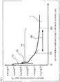
- Fig. 7 is a characteristic diagram showing the impurity concentration distribution of the FS-IGBT according to the invention. Specifically, for example, it is good when a distribution function indicating the impurity concentration distribution of the n-type FS layer 14 is, rather than a Gauss function, an exponential function such that the decay of the spatial impurity concentration is steeper than in the case of a Gauss function.
- the decrease in the impurity concentration from the position of the maximum impurity concentration to a position in which the impurity concentration is one-half of the maximum impurity concentration is steeper than in the case of a Gauss function.
- the concentration gradient when moving from a position in which the impurity concentration is sufficiently small toward the position of the maximum impurity concentration is gentler in the case of an exponential function. That is, the concentration gradient when the impurity concentration of the n-type FS layer 14 increases from the interface between the n-type FS layer 14 and n - type drift layer 1 toward the p + type collector layer 15 is gentler in the case of an exponential function distribution. Because of this, the heretofore described integrated value of the space-charge density decreases when a short circuit occurs, and it is thus possible to spread the space-charge region more quickly.
- the decay of the impurity concentration from the maximum value is steeper than in the case of a Gauss function, and that the concentration gradient is gentle when the impurity concentration increases from the interface between the n-type FS layer 14 and n - type drift layer 1 toward the p + type collector layer 15.
- n-type FS layer 14 impurity concentration distribution it is preferable to use selenium or sulfur, which have a diffusion coefficient higher than that of the normally used phosphorus or arsenic, as the n-type dopant when forming the n-type FS layer 14 by thermal diffusion.
- selenium or sulfur which have a diffusion coefficient higher than that of the normally used phosphorus or arsenic
- the impurity concentration distribution obtained by thermal diffusion of the phosphorus or arsenic normally used as the n-type dopant is well expressed by a Gauss function.
- the impurity concentration distribution of the n-type FS layer 14 when selenium or sulfur is used as the n-type dopant is such that a so-called trailing portion (trailing portion 16) can be formed in a portion deeper than a position at a depth of in the region of 10 ⁇ m from the back surface of the Si substrate.
- the trailing portion 16 is a region such that, with a position at a depth of in the region of 10 ⁇ m from the back surface of the Si substrate (hereafter referred to simply as a border position) as a border, the size of the concentration gradient in a portion deeper than the border portion (as far as a depth of in the region of 30 ⁇ m, which is the border with the n - type drift layer 1) gradually (or non-continuously) becomes smaller and gentler than the concentration gradient from the position of the maximum impurity concentration of the n-type FS layer 14 to the border position.
- the concentration gradient of the trailing portion 16 is of a smaller size.
- the trailing portion 16 is particularly noticeable in the case of selenium, and is a structure that is not seen in the impurity concentration distribution obtained from a thermal diffusion of atoms having a substitutional atomic diffusion mechanism in Si, as in the case of phosphorus and arsenic.
- the reason that the trailing portion 16 is formed is as follows. Selenium and sulfur are such that an interstitial atomic diffusion mechanism contributes dominantly to atomic diffusion, because of which a considerable ratio of the selenium or sulfur atoms implanted diffuse to the deepest part of the Si substrate. It is supposed that the trailing portion 16 of the impurity concentration distribution is formed by this selenium or sulfur diffusion.
- the integrated value of the space-charge density increases gently, as a result of which it is possible to spread the space-charge region quickly after the occurrence of a short circuit.
- the dopant for forming the n-type FS layer 14 in the invention not being limited to selenium or sulfur, it is sufficient that the dopant atoms are such that the interstitial atomic diffusion mechanism is dominant in Si.
- the dopant atoms are such that the interstitial atomic diffusion mechanism is dominant in Si.
- Li (lithium), oxygen, hydrogen, and the like are also preferable as, depending on the conditions of introduction into and diffusion in Si, they exhibit the kind of dopant concentration distribution of Fig. 7 owing to having the same advantages as selenium or sulfur.
- an FS-IGBT wherein the n-type FS layer 14 is formed with a low peak impurity concentration and diffused deeply using selenium or the like, and with a small total impurity, in order to avoid destruction due to an avalanche breakdown on the collector side, is such that thermal runaway destruction is liable to occur as a trade-off.
- the FS-IGBT according to the embodiment of the invention has a structure wherein, together with the low peak impurity concentration, deep n-type FS layer 14 formed using selenium in order to avoid short circuit destruction, the n + type buffer layer 13, in which the peak impurity concentration is controlled, is also provided between the n-type FS layer 14 and p + type collector layer 15.
- the n + type buffer layer 13 By providing the n + type buffer layer 13, the implantation of holes contributing to an increase in leakage current is suppressed, and it is thus also possible to prevent thermal runaway destruction. That is, by adopting an FS-IGBT having the n + type buffer layer 13 in which the peak impurity concentration is controlled, it is possible to prevent both short circuit destruction and thermal runaway destruction.
- the peak impurity concentration of the n + type buffer layer 13 is as previously described referring to Figs. 3 and 4 .
- an FZ n-type Si substrate of, for example, a thickness of 625 ⁇ m and resistivity of 80 ⁇ cm is prepared.
- the plurality of trenches 11 are formed, in a striped planar layout extending in a direction perpendicular to the direction in which the trenches 11 are aligned, on the front surface of the Si substrate, which is to form the n - type drift layer 1.
- the gate dielectric film 10 is formed along the inner wall of the trench 11, and the gate electrode 7, formed of polysilicon, is deposited so as to be embedded on the inner side of the gate dielectric film 10 inside the trench 11.
- the p-type base layer 5 is formed by an ion implantation of, for example, boron, using self-alignment with the gate electrode 7 as a mask.
- arsenic is selectively ion implanted into the p-type base layer 5, thereby forming the n + type emitter region 4.
- a p-type dopant is selectively ion implanted into the p-type base layer 5, thereby forming the p + type contact region 6 so as to be in contact with the n + type emitter region 4.
- an interlayer dielectric film is formed on the front surface of the Si substrate. Then, a contact hole is formed in the interlayer dielectric film for the emitter electrode 9 that straddles the p-type base layer 5 surface and n + type emitter region 4 surface.
- the thickness of the Si substrate is reduced to a desired thickness, in the region of 200 ⁇ m for example, using back grinding technology whereby grinding, polishing, etching, and the like, of the back surface of the Si substrate are combined.
- selenium or sulfur
- phosphorus is ion implanted into the thinly ground back surface of the Si substrate in order to form the n + type buffer layer 13.
- boron is ion implanted into the thinly ground back surface of the Si substrate in order to form the p + type collector layer 15.
- the thickness of the p + type collector layer 15 is less than the thickness of the n + type buffer layer 13, within a range of 0.2 ⁇ m to 1.0 ⁇ m.
- the dopants implanted into the back surface of the Si substrate in order to form the three layers of the n-type FS layer 14, n + type buffer layer 13, and p + type collector layer 15 are simultaneously activated. Specifically, it is possible to achieve an efficient process by carrying out heat treatment for a time within a range of 0.5 hours to 5 hours, for example, 2 hours, at a temperature within a range of 750°C to 950°C, for example, 830°C, thereby simultaneously activating the dopants implanted in order to form the aforementioned three layers.
- Al-Si electrode film metal electrode film
- Al-Si electrode film metal electrode film
- the FS-IGBT chip is such that the front surface side Al-Si electrode film in contact with the n + type emitter region 4 and Al-Si electrode film electrically in contact with the gate electrode 7 are each connected to an external connection terminal by ultrasonic bonding with an Al wire. Also, the FS-IGBT chip is such that the back surface side collector electrode 8 is fixed by soldering to a heat releasing substrate such as a copper substrate (not shown). Subsequently, the FS-IGBT chip is packaged, whereby the FS-IGBT semiconductor device is completed.
- the impurity concentration and thickness (or diffusion depth) of each layer described thus far can be obtained by measuring the spread resistance using, for example, a heretofore known spread resistance measuring instrument, and converting from the spread resistance value.
- the amount of holes implanted from the collector side when a short circuit occurs increases, and the rise of a magnetic field intensity on the collector side is suppressed, by forming an n-type FS layer that is deep and of a low impurity concentration, and that has a gentle concentration gradient, using selenium or sulfur as a dopant. Also, by providing an n + type buffer layer having a predetermined peak impurity concentration between the n-type FS layer and p + type collector layer using an ion implantation of phosphorus, it is possible to suppress an implantation into the n-type FS layer of holes contributing to an increase in leakage current.
- the peak impurity concentration of the n + type buffer layer is at least one digit lower than the peak impurity concentration of the p + type collector layer.
- the invention has been described with a trench-FS-IGBT as an example but, the heretofore described embodiment not being limiting, various changes are possible without departing from the scope of the invention as defined by the appended claims. Specifically, the invention can also be applied to, for example, a planar gate FS-IGBT. Also, a description has been given of an FS-IGBT with a breakdown voltage (rated voltage) of 1,700V or more but, the invention not being limited to the heretofore described embodiment, the invention can also be applied to an element with a breakdown voltage such that the rated voltage exceeds 600V.
- rated voltage rated voltage
- the semiconductor device and semiconductor device manufacturing method according to the invention are useful in power semiconductor devices used in the field of industrial instruments such as general purpose and electric vehicle inverters and AC servos, uninterruptible power supplies (UPS), and switching power supplies, and in the field of consumer instruments such as microwave cookers, rice cookers, and stroboscopes.
- industrial instruments such as general purpose and electric vehicle inverters and AC servos, uninterruptible power supplies (UPS), and switching power supplies
- UPS uninterruptible power supplies
- switching power supplies and in the field of consumer instruments
- microwave cookers such as microwave cookers, rice cookers, and stroboscopes.
Landscapes
- Electrodes Of Semiconductors (AREA)
- Thyristors (AREA)
- Metal-Oxide And Bipolar Metal-Oxide Semiconductor Integrated Circuits (AREA)
Claims (9)
- Dispositif à semi-conducteur comprenant:une couche de dérive d'un premier type de conductivité (1) formée par un substrat semi-conducteur d'un premier type de conductivité;une couche de base d'un deuxième type de conductivité (5) formée dans une couche de surface d'une surface principale du substrat semi-conducteur de premier type de conductivité;une couche d'émission de deuxième type de conductivité (4) formée dans une couche de surface sur le côté de cette surface principale du substrat semi-conducteur de premier type de conductivité de la couche de base de deuxième type de conductivité (5);un film diélectrique de grille (10) fourni sur cette surface principale du substrat semi-conducteur de premier type de conductivité et en contact avec la couche d'émission de premier type de conductivité (4), la couche de base de deuxième type de conductivité (5), et la couche de dérive de premier type de conductivité (1);une électrode de grille (7) tournée vers la couche d'émission de premier type de conductivité (4), la couche de base de deuxième type de conductivité (5), et la couche de dérive de premier type de conductivité (1) avec le film diélectrique de grille (10) intercalé entre celles-ci;une structure de grille MOS (12) formée par la couche de dérive de premier type de conductivité (1), la couche de base de deuxième type de conductivité (5), la couche d'émission de premier type de conductivité (4), le film diélectrique de grille (10), et l'électrode de grille (7);une couche de collecte de deuxième type de conductivité (15) fournie sur l'autre surface principale du substrat semi-conducteur de premier type de conductivité;une couche d'arrêt de champ de premier type de conductivité (14) fournie entre la couche de dérive de premier type de conductivité (1) et la couche de collecte de deuxième type de conductivité (15) et ayant une concentration d'impuretés supérieure à celle de la couche de dérive de premier type de conductivité (1); etune couche tampon de premier type de conductivité (13) fournie entre la couche d'arrêt de champ de premier type de conductivité (14) et la couche de collecte de deuxième type de conductivité (15), dans lequella concentration d'impuretés maximale de la couche d'arrêt de champ de premier type de conductivité (14) est dans les limites d'une plage de 3 x 104cm-3 à 3 x 105cm-3,la profondeur de la couche d'arrêt de champ de premier type de conductivité (14) à partir de l'autre surface principale du substrat semi-conducteur de premier type de conductivité est comprise entre 20 µm et 40 µm, etla concentration d'impuretés maximale de la couche tampon de premier type de conductivité (13) est supérieure à la concentration d'impuretés maximale de la couche d'arrêt de champ de premier type de conductivité (14) et est supérieure à 6 x 105cm-3,l'épaisseur de la couche tampon de premier type de conductivité (13) est comprise entre 0,5pm et 3,0µm,l'épaisseur de la couche de collecte de deuxième type de conductivité (15) est inférieure à l'épaisseur de la couche tampon de premier type de conductivité (13) et est comprise entre 0,2µm et 1,0µm,la répartition de la concentration d'impuretés de la couche d'arrêt de champ de premier type de conductivité (14) a un gradient de concentration qui diminue via la totalité de la couche d'arrêt de champ de premier type de conductivité (14) à partir du côté de l'autre surface principale du substrat semi-conducteur de premier type de conductivité jusqu'au côté de cette surface principale du substrat semi-conducteur de premier type de conductivité,caractérisé en ce quela concentration d'impuretés maximale de la couche tampon de premier type de conductivité (13) est d'un dixième ou moins de la concentration d'impuretés maximale de la couche de collecte de deuxième type de conductivité (15).
- Dispositif à semi-conducteur selon la revendication 1, caractérisé en ce que la répartition de la concentration d'impuretés de la couche d'arrêt de champ de premier type de conductivité (14)
a un premier gradient de concentration d'impuretés dans une première partie depuis le côté de la couche de collecte de deuxième type de conductivité (15) jusqu'au côté de la couche de dérive de premier type de conductivité, et
a un deuxième gradient de concentration d'impuretés dans une deuxième partie plus en profondeur vers le côté de couche de dérive de premier type de conductivité que la première partie,
dans lequel le premier gradient de concentration d'impuretés dans la première partie est supérieur au deuxième gradient de concentration d'impuretés dans la deuxième partie. - Dispositif à semi-conducteur selon la revendication 1, caractérisé en ce que la concentration d'impuretés maximale de la couche de collecte de deuxième type de conductivité est dans les limites d'une plage de 6 x 1016cm-3 à 1 x 1020cm-3.
- Dispositif à semi-conducteur selon la revendication 1, caractérisé en ce que le dopant de la couche d'arrêt de champ de premier type de conductivité (14) est du sélénium ou du soufre.
- Dispositif à semi-conducteur selon la revendication 1, caractérisé en ce que le dopant de la couche tampon de premier type de conductivité (13) est du phosphore.
- Dispositif à semi-conducteur selon la revendication 1, caractérisé en ce que la concentration d'impuretés dans la couche d'arrêt de champ de premier type de conductivité (14) diminue progressivement à partir d'une position de la concentration d'impuretés maximale de la couche d'arrêt de champ de premier type de conductivité (14) jusqu'au côté de cette surface principale du substrat semi-conducteur de premier type de conductivité.
- Dispositif à semi-conducteur selon la revendication 1 ou 6, caractérisé en ce que la tension nominale est de 1,200V ou plus.
- Procédé de fabrication d'un dispositif à semi-conducteur comprenant
une couche de dérive de premier type de conductivité (1) formée par un substrat semi-conducteur de premier type de conductivité,
une structure de grille MOS (12) formée par au moins une électrode de grille (7),
un film diélectrique de grille (10), et le substrat semi-conducteur de premier type de conductivité fourni sur un côté de surface principale du substrat semi-conducteur de premier type de conductivité,
une couche de collecte de deuxième type de conductivité (15) fournie sur l'autre surface principale du substrat semi-conducteur de premier type de conductivité, l'épaisseur de la couche de collecte de deuxième type de conductivité (15) étant comprise entre 0,2pm et 1,0µm,
une couche d'arrêt de champ de premier type de conductivité (14) fournie entre la couche de dérive de premier type de conductivité (1) et la couche de collecte de deuxième type de conductivité (15) et ayant une concentration d'impuretés supérieure à celle de la couche de dérive de premier type de conductivité (1), la concentration d'impuretés maximale de la couche d'arrêt de champ de premier type de conductivité (14) étant dans les limites d'une plage de 3 x 10¹⁴Cm-3 à 3 x 1015cm-3,
la profondeur de la couche d'arrêt de champ de premier type de conductivité (14) à partir de l'autre surface principale du substrat semi-conducteur de premier type de conductivité est comprise entre 20 µm et 40 µm, et
une couche tampon de premier type de conductivité (13) fournie entre la couche d'arrêt de champ de premier type de conductivité (14) et une couche de collecte de deuxième type de conductivité (15) et ayant une concentration d'impuretés supérieure à celle de la couche d'arrêt de champ de premier type de conductivité (14),
dans lequel la concentration d'impuretés maximale de la couche tampon de premier type de conductivité (13) est supérieure à 6 x 10¹⁵Cm-3, et
l'épaisseur de la couche tampon de premier type de conductivité (13) étant comprise entre 0,5pm et 3,0µm, et
l'épaisseur de la couche de collecte de deuxième type de conductivité (15) est inférieure à l'épaisseur de la couche tampon de premier type de conductivité (13),
le procédé de fabrication comprenant:une étape de formation de structure de grille MOS consistant à former la structure de grille MOS (12) sur le côté de cette surface principale du substrat semi-conducteur de premier type de conductivité;une étape d'amincissement de substrat consistant à rectifier l'autre surface principale du substrat semi-conducteur de premier type de conductivité pour réduire une épaisseur du substrat semi-conducteur de premier type de conductivité à une épaisseur prédéterminée;une étape d'implantation consistant en une implantation ionique de dopants dans la surface rectifiée du substrat semi-conducteur de premier type de conductivité afin de former chacune parmi la couche d'arrêt de champ de premier type de conductivité (14), la couche tampon de premier type de conductivité (13), et la couche de collecte de deuxième type de conductivité (15);une étape d'activation, de réalisation d'un traitement thermique pour simultanément activer électriquement la pluralité des ions dopants implantés dans la surface rectifiée du substrat semi-conducteur de premier type de conductivité; etune étape de formation de film d'électrode consistant à former un film d'électrode métallique par pulvérisation cathodique sur cette surface principale du substrat semi-conducteur de premier type de conductivité et à réaliser un traitement thermique,dans lequell'étape d'implantation et l'étape d'activation sont réalisées de manière à ce que la répartition de la concentration d'impuretés de la couche d'arrêt de champ de premier type de conductivité (14) a un gradient de concentration qui diminue via la totalité de la couche d'arrêt de champ de premier type de conductivité (14) à partir du côté de l'autre surface principale du substrat semi-conducteur de premier type de conductivité jusqu'au côté de cette surface principale du substrat semi-conducteur de premier type de conductivité,le procédé se caractérisant en ce quela concentration d'impuretés maximale de la couche tampon de premier type de conductivité (13) est de un dixième ou moins de la concentration d'impuretés maximale de la couche de collecte de deuxième type de conductivité (15). - Procédé de fabrication d'un dispositif à semi-conducteur selon la revendication 8,
caractérisé en ce que du sélénium pour former la couche d'arrêt de champ de premier type de conductivité (14), du phosphore pour former la couche tampon de premier type de conductivité (13), et du bore pour former la couche de collecte de deuxième type de conductivité (15) font l'objet d'une implantation séquentielle d'ions en tant qu'une pluralité de dopants dans l'étape d'implantation, et
la pluralité des dopants sont activés simultanément par le traitement thermique dans l'étape d'activation.
Applications Claiming Priority (2)
| Application Number | Priority Date | Filing Date | Title |
|---|---|---|---|
| JP2011111709 | 2011-05-18 | ||
| PCT/JP2012/062875 WO2012157772A1 (fr) | 2011-05-18 | 2012-05-18 | Dispositif à semiconducteur et procédé de fabrication d'un dispositif à semiconducteur |
Publications (3)
| Publication Number | Publication Date |
|---|---|
| EP2711986A1 EP2711986A1 (fr) | 2014-03-26 |
| EP2711986A4 EP2711986A4 (fr) | 2014-11-12 |
| EP2711986B1 true EP2711986B1 (fr) | 2020-08-19 |
Family
ID=47177086
Family Applications (1)
| Application Number | Title | Priority Date | Filing Date |
|---|---|---|---|
| EP12785949.4A Active EP2711986B1 (fr) | 2011-05-18 | 2012-05-18 | Dispositif à semiconducteur et procédé de fabrication d'un dispositif à semiconducteur |
Country Status (5)
| Country | Link |
|---|---|
| US (3) | US9324847B2 (fr) |
| EP (1) | EP2711986B1 (fr) |
| JP (1) | JP5874723B2 (fr) |
| CN (2) | CN106128946B (fr) |
| WO (1) | WO2012157772A1 (fr) |
Families Citing this family (35)
| Publication number | Priority date | Publication date | Assignee | Title |
|---|---|---|---|---|
| JP5874723B2 (ja) | 2011-05-18 | 2016-03-02 | 富士電機株式会社 | 半導体装置および半導体装置の製造方法 |
| JP5817686B2 (ja) * | 2011-11-30 | 2015-11-18 | 株式会社デンソー | 半導体装置 |
| WO2013141181A1 (fr) | 2012-03-23 | 2013-09-26 | 富士電機株式会社 | Dispositif à semiconducteur et procédé de fabrication d'un dispositif à semiconducteur |
| KR102198982B1 (ko) * | 2013-03-28 | 2021-01-07 | 에이비비 슈바이쯔 아게 | 절연 게이트 바이폴라 트랜지스터를 제조하기 위한 방법 |
| JP5971414B2 (ja) * | 2013-06-12 | 2016-08-17 | 三菱電機株式会社 | 半導体装置 |
| US9331197B2 (en) * | 2013-08-08 | 2016-05-03 | Cree, Inc. | Vertical power transistor device |
| JP2015046502A (ja) * | 2013-08-28 | 2015-03-12 | 住友電気工業株式会社 | 炭化珪素半導体装置およびその製造方法 |
| US10600903B2 (en) | 2013-09-20 | 2020-03-24 | Cree, Inc. | Semiconductor device including a power transistor device and bypass diode |
| US10868169B2 (en) | 2013-09-20 | 2020-12-15 | Cree, Inc. | Monolithically integrated vertical power transistor and bypass diode |
| CN104716039B (zh) * | 2013-12-13 | 2018-02-06 | 上海华虹宏力半导体制造有限公司 | 提高igbt性能的背面工艺制作方法 |
| JP6194812B2 (ja) * | 2014-02-18 | 2017-09-13 | トヨタ自動車株式会社 | 半導体モジュール |
| JP6287407B2 (ja) | 2014-03-19 | 2018-03-07 | サンケン電気株式会社 | 半導体装置 |
| JP2015201476A (ja) * | 2014-04-04 | 2015-11-12 | 三菱電機株式会社 | 半導体装置およびその製造方法 |
| JP6332446B2 (ja) | 2014-06-12 | 2018-05-30 | 富士電機株式会社 | 半導体装置 |
| JP6319454B2 (ja) * | 2014-10-24 | 2018-05-09 | 富士電機株式会社 | 半導体装置および半導体装置の製造方法 |
| DE112015006059T5 (de) | 2015-01-27 | 2017-10-12 | Mitsubishi Electric Corporation | Halbleitervorrichtung |
| US10411093B2 (en) | 2015-12-28 | 2019-09-10 | Mitsubishi Electric Corporation | Semiconductor device and method for manufacturing semiconductor device |
| US9768285B1 (en) | 2016-03-16 | 2017-09-19 | Semiconductor Components Industries, Llc | Semiconductor device and method of manufacture |
| CN107218176B (zh) | 2016-03-21 | 2020-05-19 | 通用电气公司 | 风力节距调整系统 |
| JP2016195271A (ja) * | 2016-07-04 | 2016-11-17 | 三菱電機株式会社 | 半導体装置 |
| WO2018135448A1 (fr) * | 2017-01-17 | 2018-07-26 | 富士電機株式会社 | Dispositif à semi-conducteur |
| JP6661575B2 (ja) * | 2017-06-20 | 2020-03-11 | 三菱電機株式会社 | 半導体装置およびその製造方法 |
| CN107731901B (zh) * | 2017-11-20 | 2024-02-23 | 电子科技大学 | 一种逆阻型igbt |
| DE102017128243B4 (de) | 2017-11-29 | 2021-09-23 | Infineon Technologies Ag | Bipolartransistor mit isoliertem gate, aufweisend erste und zweite feldstoppzonenbereiche, und herstellungsverfahren |
| CN108054201A (zh) * | 2017-12-27 | 2018-05-18 | 无锡新洁能股份有限公司 | 一种抗耐压冲击软关断的igbt器件结构及其制造方法 |
| JP7010184B2 (ja) * | 2018-09-13 | 2022-01-26 | 株式会社デンソー | 半導体装置 |
| CN109712885A (zh) * | 2018-12-17 | 2019-05-03 | 成都森未科技有限公司 | 一种半导体器件缓冲层制造方法 |
| CN110502049B (zh) * | 2019-08-30 | 2021-05-07 | 北京北方华创微电子装备有限公司 | 卡盘温度控制方法、卡盘温度控制系统及半导体设备 |
| CN112582469A (zh) * | 2019-09-29 | 2021-03-30 | 比亚迪半导体股份有限公司 | 衬底、半导体器件及其制备方法 |
| DE112021000205T5 (de) | 2020-07-15 | 2022-08-18 | Fuji Electric Co., Ltd. | Halbleitervorrichtung |
| JP7494745B2 (ja) * | 2021-01-26 | 2024-06-04 | 三菱電機株式会社 | 半導体装置および半導体装置の製造方法 |
| CN116978937A (zh) * | 2021-02-07 | 2023-10-31 | 华为技术有限公司 | 半导体器件及相关模块、电路、制备方法 |
| EP4258364A1 (fr) * | 2022-04-04 | 2023-10-11 | Infineon Technologies AG | Dispositif semi-conducteur à large bande interdite et son procédé de fabrication |
| JP7796611B2 (ja) * | 2022-08-23 | 2026-01-09 | 三菱電機株式会社 | 半導体装置、半導体装置の製造方法、および電力変換装置 |
| CN121604468B (zh) * | 2026-01-28 | 2026-04-03 | 深圳辰达半导体有限公司 | 含渐变掺杂外延层的新型分裂栅mos管及其制备方法 |
Family Cites Families (23)
| Publication number | Priority date | Publication date | Assignee | Title |
|---|---|---|---|---|
| JPH09121052A (ja) * | 1995-08-21 | 1997-05-06 | Fuji Electric Co Ltd | 半導体装置およびその製造方法 |
| WO2000004596A2 (fr) | 1998-07-17 | 2000-01-27 | Infineon Technologies Ag | Composant a semi-conducteur de puissance pour tensions de blocage elevees |
| DE19981344D2 (de) | 1998-07-17 | 2001-08-30 | Siemens Ag | Leistungshalbleiterelement mit einem Emitterbereich, dem eine Stoppzone vorgelagert ist |
| US7084456B2 (en) * | 1999-05-25 | 2006-08-01 | Advanced Analogic Technologies, Inc. | Trench MOSFET with recessed clamping diode using graded doping |
| JP4581179B2 (ja) * | 2000-04-26 | 2010-11-17 | 富士電機システムズ株式会社 | 絶縁ゲート型半導体装置 |
| DE10205324B4 (de) | 2001-02-09 | 2012-04-19 | Fuji Electric Co., Ltd. | Halbleiterbauelement |
| JP3687614B2 (ja) | 2001-02-09 | 2005-08-24 | 富士電機デバイステクノロジー株式会社 | 半導体装置 |
| DE10205323B4 (de) | 2001-02-09 | 2011-03-24 | Fuji Electric Systems Co., Ltd. | Verfahren zur Herstellung eines Halbleiterbauelements |
| JP3885598B2 (ja) * | 2001-02-09 | 2007-02-21 | 富士電機デバイステクノロジー株式会社 | 半導体装置の製造方法 |
| JP3764343B2 (ja) | 2001-02-28 | 2006-04-05 | 株式会社東芝 | 半導体装置の製造方法 |
| JP5160001B2 (ja) | 2001-04-02 | 2013-03-13 | 富士電機株式会社 | 半導体装置の製造方法 |
| JP2004079878A (ja) * | 2002-08-21 | 2004-03-11 | Toshiba Corp | 半導体装置及びその製造方法 |
| JP3951868B2 (ja) * | 2002-09-12 | 2007-08-01 | 富士電機デバイステクノロジー株式会社 | 半導体装置およびその製造方法 |
| JP2004311481A (ja) * | 2003-04-02 | 2004-11-04 | Toshiba Corp | 半導体装置 |
| DE102006046845B4 (de) * | 2006-10-02 | 2013-12-05 | Infineon Technologies Austria Ag | Halbleiterbauelement mit verbesserter Robustheit |
| JP5228308B2 (ja) | 2006-10-19 | 2013-07-03 | 富士電機株式会社 | 半導体装置の製造方法 |
| JP5320679B2 (ja) * | 2007-02-28 | 2013-10-23 | 富士電機株式会社 | 半導体装置およびその製造方法 |
| JP5365009B2 (ja) * | 2008-01-23 | 2013-12-11 | 富士電機株式会社 | 半導体装置およびその製造方法 |
| JP2010056134A (ja) | 2008-08-26 | 2010-03-11 | Mitsubishi Electric Corp | 半導体装置 |
| US20100155831A1 (en) * | 2008-12-20 | 2010-06-24 | Power Integrations, Inc. | Deep trench insulated gate bipolar transistor |
| US8101528B2 (en) * | 2009-08-07 | 2012-01-24 | Varian Semiconductor Equipment Associates, Inc. | Low temperature ion implantation |
| JP5569532B2 (ja) | 2009-11-02 | 2014-08-13 | 富士電機株式会社 | 半導体装置および半導体装置の製造方法 |
| JP5874723B2 (ja) | 2011-05-18 | 2016-03-02 | 富士電機株式会社 | 半導体装置および半導体装置の製造方法 |
-
2012
- 2012-05-18 JP JP2013515238A patent/JP5874723B2/ja active Active
- 2012-05-18 CN CN201610702029.3A patent/CN106128946B/zh active Active
- 2012-05-18 WO PCT/JP2012/062875 patent/WO2012157772A1/fr not_active Ceased
- 2012-05-18 CN CN201280023905.XA patent/CN103534811B/zh active Active
- 2012-05-18 EP EP12785949.4A patent/EP2711986B1/fr active Active
-
2013
- 2013-11-13 US US14/079,072 patent/US9324847B2/en active Active
-
2016
- 2016-03-15 US US15/070,429 patent/US9812561B2/en active Active
- 2016-03-30 US US15/084,549 patent/US9818852B2/en active Active
Non-Patent Citations (1)
| Title |
|---|
| None * |
Also Published As
| Publication number | Publication date |
|---|---|
| EP2711986A1 (fr) | 2014-03-26 |
| US20160197170A1 (en) | 2016-07-07 |
| US20140070268A1 (en) | 2014-03-13 |
| CN106128946A (zh) | 2016-11-16 |
| US9818852B2 (en) | 2017-11-14 |
| US9324847B2 (en) | 2016-04-26 |
| WO2012157772A1 (fr) | 2012-11-22 |
| CN106128946B (zh) | 2019-03-08 |
| US20160211356A1 (en) | 2016-07-21 |
| CN103534811B (zh) | 2016-09-21 |
| EP2711986A4 (fr) | 2014-11-12 |
| JPWO2012157772A1 (ja) | 2014-07-31 |
| JP5874723B2 (ja) | 2016-03-02 |
| CN103534811A (zh) | 2014-01-22 |
| US9812561B2 (en) | 2017-11-07 |
Similar Documents
| Publication | Publication Date | Title |
|---|---|---|
| EP2711986B1 (fr) | Dispositif à semiconducteur et procédé de fabrication d'un dispositif à semiconducteur | |
| US20240047200A1 (en) | Semiconductor device and method for manufacturing the same | |
| JP7147891B2 (ja) | 半導体装置 | |
| US8003502B2 (en) | Semiconductor device and fabrication method | |
| JP7271659B2 (ja) | 絶縁ゲートパワー半導体装置、およびそのような装置を製造するための方法 | |
| US10593789B2 (en) | Semiconductor apparatus and method of manufacturing the same | |
| CN103531450B (zh) | 用于形成横向变化掺杂浓度的方法和半导体器件 | |
| CN108074977A (zh) | 半导体装置及其制造方法 | |
| CN110419111B (zh) | 自对准且稳健的绝缘栅双极晶体管器件 | |
| JP2024102269A (ja) | 半導体部品および半導体部品の製造方法 | |
| WO2013146329A1 (fr) | Semi-conducteur résistant à une tension élevée | |
| US20170294527A1 (en) | Semiconductor device and method for manufacturing the same |
Legal Events
| Date | Code | Title | Description |
|---|---|---|---|
| PUAI | Public reference made under article 153(3) epc to a published international application that has entered the european phase |
Free format text: ORIGINAL CODE: 0009012 |
|
| 17P | Request for examination filed |
Effective date: 20131218 |
|
| AK | Designated contracting states |
Kind code of ref document: A1 Designated state(s): AL AT BE BG CH CY CZ DE DK EE ES FI FR GB GR HR HU IE IS IT LI LT LU LV MC MK MT NL NO PL PT RO RS SE SI SK SM TR |
|
| DAX | Request for extension of the european patent (deleted) | ||
| A4 | Supplementary search report drawn up and despatched |
Effective date: 20141014 |
|
| RIC1 | Information provided on ipc code assigned before grant |
Ipc: H01L 21/336 20060101ALI20141008BHEP Ipc: H01L 29/78 20060101ALI20141008BHEP Ipc: H01L 29/739 20060101AFI20141008BHEP |
|
| STAA | Information on the status of an ep patent application or granted ep patent |
Free format text: STATUS: EXAMINATION IS IN PROGRESS |
|
| 17Q | First examination report despatched |
Effective date: 20190115 |
|
| GRAP | Despatch of communication of intention to grant a patent |
Free format text: ORIGINAL CODE: EPIDOSNIGR1 |
|
| RIC1 | Information provided on ipc code assigned before grant |
Ipc: H01L 29/08 20060101ALI20200127BHEP Ipc: H01L 29/78 20060101ALI20200127BHEP Ipc: H01L 21/336 20060101ALI20200127BHEP Ipc: H01L 29/36 20060101ALI20200127BHEP Ipc: H01L 29/739 20060101AFI20200127BHEP |
|
| STAA | Information on the status of an ep patent application or granted ep patent |
Free format text: STATUS: GRANT OF PATENT IS INTENDED |
|
| INTG | Intention to grant announced |
Effective date: 20200305 |
|
| GRAS | Grant fee paid |
Free format text: ORIGINAL CODE: EPIDOSNIGR3 |
|
| GRAA | (expected) grant |
Free format text: ORIGINAL CODE: 0009210 |
|
| STAA | Information on the status of an ep patent application or granted ep patent |
Free format text: STATUS: THE PATENT HAS BEEN GRANTED |
|
| AK | Designated contracting states |
Kind code of ref document: B1 Designated state(s): AL AT BE BG CH CY CZ DE DK EE ES FI FR GB GR HR HU IE IS IT LI LT LU LV MC MK MT NL NO PL PT RO RS SE SI SK SM TR |
|
| REG | Reference to a national code |
Ref country code: GB Ref legal event code: FG4D |
|
| RIN1 | Information on inventor provided before grant (corrected) |
Inventor name: YOSHIMURA, TAKASHI Inventor name: NAKANO, HAYATO Inventor name: OZAKI, DAISUKE Inventor name: ONOZAWA, YUICHI Inventor name: KURIBAYASHI, HIDENAO |
|
| REG | Reference to a national code |
Ref country code: CH Ref legal event code: EP |
|
| REG | Reference to a national code |
Ref country code: DE Ref legal event code: R096 Ref document number: 602012071884 Country of ref document: DE |
|
| REG | Reference to a national code |
Ref country code: AT Ref legal event code: REF Ref document number: 1304927 Country of ref document: AT Kind code of ref document: T Effective date: 20200915 |
|
| REG | Reference to a national code |
Ref country code: IE Ref legal event code: FG4D |
|
| REG | Reference to a national code |
Ref country code: LT Ref legal event code: MG4D |
|
| REG | Reference to a national code |
Ref country code: NL Ref legal event code: MP Effective date: 20200819 |
|
| PG25 | Lapsed in a contracting state [announced via postgrant information from national office to epo] |
Ref country code: LT Free format text: LAPSE BECAUSE OF FAILURE TO SUBMIT A TRANSLATION OF THE DESCRIPTION OR TO PAY THE FEE WITHIN THE PRESCRIBED TIME-LIMIT Effective date: 20200819 Ref country code: HR Free format text: LAPSE BECAUSE OF FAILURE TO SUBMIT A TRANSLATION OF THE DESCRIPTION OR TO PAY THE FEE WITHIN THE PRESCRIBED TIME-LIMIT Effective date: 20200819 Ref country code: GR Free format text: LAPSE BECAUSE OF FAILURE TO SUBMIT A TRANSLATION OF THE DESCRIPTION OR TO PAY THE FEE WITHIN THE PRESCRIBED TIME-LIMIT Effective date: 20201120 Ref country code: SE Free format text: LAPSE BECAUSE OF FAILURE TO SUBMIT A TRANSLATION OF THE DESCRIPTION OR TO PAY THE FEE WITHIN THE PRESCRIBED TIME-LIMIT Effective date: 20200819 Ref country code: BG Free format text: LAPSE BECAUSE OF FAILURE TO SUBMIT A TRANSLATION OF THE DESCRIPTION OR TO PAY THE FEE WITHIN THE PRESCRIBED TIME-LIMIT Effective date: 20201119 Ref country code: PT Free format text: LAPSE BECAUSE OF FAILURE TO SUBMIT A TRANSLATION OF THE DESCRIPTION OR TO PAY THE FEE WITHIN THE PRESCRIBED TIME-LIMIT Effective date: 20201221 Ref country code: FI Free format text: LAPSE BECAUSE OF FAILURE TO SUBMIT A TRANSLATION OF THE DESCRIPTION OR TO PAY THE FEE WITHIN THE PRESCRIBED TIME-LIMIT Effective date: 20200819 Ref country code: NO Free format text: LAPSE BECAUSE OF FAILURE TO SUBMIT A TRANSLATION OF THE DESCRIPTION OR TO PAY THE FEE WITHIN THE PRESCRIBED TIME-LIMIT Effective date: 20201119 |
|
| REG | Reference to a national code |
Ref country code: AT Ref legal event code: MK05 Ref document number: 1304927 Country of ref document: AT Kind code of ref document: T Effective date: 20200819 |
|
| PG25 | Lapsed in a contracting state [announced via postgrant information from national office to epo] |
Ref country code: RS Free format text: LAPSE BECAUSE OF FAILURE TO SUBMIT A TRANSLATION OF THE DESCRIPTION OR TO PAY THE FEE WITHIN THE PRESCRIBED TIME-LIMIT Effective date: 20200819 Ref country code: LV Free format text: LAPSE BECAUSE OF FAILURE TO SUBMIT A TRANSLATION OF THE DESCRIPTION OR TO PAY THE FEE WITHIN THE PRESCRIBED TIME-LIMIT Effective date: 20200819 Ref country code: NL Free format text: LAPSE BECAUSE OF FAILURE TO SUBMIT A TRANSLATION OF THE DESCRIPTION OR TO PAY THE FEE WITHIN THE PRESCRIBED TIME-LIMIT Effective date: 20200819 Ref country code: PL Free format text: LAPSE BECAUSE OF FAILURE TO SUBMIT A TRANSLATION OF THE DESCRIPTION OR TO PAY THE FEE WITHIN THE PRESCRIBED TIME-LIMIT Effective date: 20200819 Ref country code: IS Free format text: LAPSE BECAUSE OF FAILURE TO SUBMIT A TRANSLATION OF THE DESCRIPTION OR TO PAY THE FEE WITHIN THE PRESCRIBED TIME-LIMIT Effective date: 20201219 |
|
| PG25 | Lapsed in a contracting state [announced via postgrant information from national office to epo] |
Ref country code: CZ Free format text: LAPSE BECAUSE OF FAILURE TO SUBMIT A TRANSLATION OF THE DESCRIPTION OR TO PAY THE FEE WITHIN THE PRESCRIBED TIME-LIMIT Effective date: 20200819 Ref country code: EE Free format text: LAPSE BECAUSE OF FAILURE TO SUBMIT A TRANSLATION OF THE DESCRIPTION OR TO PAY THE FEE WITHIN THE PRESCRIBED TIME-LIMIT Effective date: 20200819 Ref country code: DK Free format text: LAPSE BECAUSE OF FAILURE TO SUBMIT A TRANSLATION OF THE DESCRIPTION OR TO PAY THE FEE WITHIN THE PRESCRIBED TIME-LIMIT Effective date: 20200819 Ref country code: SM Free format text: LAPSE BECAUSE OF FAILURE TO SUBMIT A TRANSLATION OF THE DESCRIPTION OR TO PAY THE FEE WITHIN THE PRESCRIBED TIME-LIMIT Effective date: 20200819 Ref country code: RO Free format text: LAPSE BECAUSE OF FAILURE TO SUBMIT A TRANSLATION OF THE DESCRIPTION OR TO PAY THE FEE WITHIN THE PRESCRIBED TIME-LIMIT Effective date: 20200819 |
|
| REG | Reference to a national code |
Ref country code: DE Ref legal event code: R097 Ref document number: 602012071884 Country of ref document: DE |
|
| PG25 | Lapsed in a contracting state [announced via postgrant information from national office to epo] |
Ref country code: AL Free format text: LAPSE BECAUSE OF FAILURE TO SUBMIT A TRANSLATION OF THE DESCRIPTION OR TO PAY THE FEE WITHIN THE PRESCRIBED TIME-LIMIT Effective date: 20200819 Ref country code: AT Free format text: LAPSE BECAUSE OF FAILURE TO SUBMIT A TRANSLATION OF THE DESCRIPTION OR TO PAY THE FEE WITHIN THE PRESCRIBED TIME-LIMIT Effective date: 20200819 Ref country code: ES Free format text: LAPSE BECAUSE OF FAILURE TO SUBMIT A TRANSLATION OF THE DESCRIPTION OR TO PAY THE FEE WITHIN THE PRESCRIBED TIME-LIMIT Effective date: 20200819 |
|
| PLBE | No opposition filed within time limit |
Free format text: ORIGINAL CODE: 0009261 |
|
| STAA | Information on the status of an ep patent application or granted ep patent |
Free format text: STATUS: NO OPPOSITION FILED WITHIN TIME LIMIT |
|
| PG25 | Lapsed in a contracting state [announced via postgrant information from national office to epo] |
Ref country code: SK Free format text: LAPSE BECAUSE OF FAILURE TO SUBMIT A TRANSLATION OF THE DESCRIPTION OR TO PAY THE FEE WITHIN THE PRESCRIBED TIME-LIMIT Effective date: 20200819 |
|
| 26N | No opposition filed |
Effective date: 20210520 |
|
| PG25 | Lapsed in a contracting state [announced via postgrant information from national office to epo] |
Ref country code: IT Free format text: LAPSE BECAUSE OF FAILURE TO SUBMIT A TRANSLATION OF THE DESCRIPTION OR TO PAY THE FEE WITHIN THE PRESCRIBED TIME-LIMIT Effective date: 20200819 |
|
| PG25 | Lapsed in a contracting state [announced via postgrant information from national office to epo] |
Ref country code: SI Free format text: LAPSE BECAUSE OF FAILURE TO SUBMIT A TRANSLATION OF THE DESCRIPTION OR TO PAY THE FEE WITHIN THE PRESCRIBED TIME-LIMIT Effective date: 20200819 |
|
| REG | Reference to a national code |
Ref country code: CH Ref legal event code: PL |
|
| GBPC | Gb: european patent ceased through non-payment of renewal fee |
Effective date: 20210518 |
|
| PG25 | Lapsed in a contracting state [announced via postgrant information from national office to epo] |
Ref country code: LU Free format text: LAPSE BECAUSE OF NON-PAYMENT OF DUE FEES Effective date: 20210518 Ref country code: LI Free format text: LAPSE BECAUSE OF NON-PAYMENT OF DUE FEES Effective date: 20210531 Ref country code: MC Free format text: LAPSE BECAUSE OF FAILURE TO SUBMIT A TRANSLATION OF THE DESCRIPTION OR TO PAY THE FEE WITHIN THE PRESCRIBED TIME-LIMIT Effective date: 20200819 Ref country code: CH Free format text: LAPSE BECAUSE OF NON-PAYMENT OF DUE FEES Effective date: 20210531 |
|
| REG | Reference to a national code |
Ref country code: BE Ref legal event code: MM Effective date: 20210531 |
|
| PG25 | Lapsed in a contracting state [announced via postgrant information from national office to epo] |
Ref country code: IE Free format text: LAPSE BECAUSE OF NON-PAYMENT OF DUE FEES Effective date: 20210518 Ref country code: GB Free format text: LAPSE BECAUSE OF NON-PAYMENT OF DUE FEES Effective date: 20210518 |
|
| PG25 | Lapsed in a contracting state [announced via postgrant information from national office to epo] |
Ref country code: BE Free format text: LAPSE BECAUSE OF NON-PAYMENT OF DUE FEES Effective date: 20210531 |
|
| REG | Reference to a national code |
Ref country code: FR Ref legal event code: PLFP Year of fee payment: 12 |
|
| PG25 | Lapsed in a contracting state [announced via postgrant information from national office to epo] |
Ref country code: HU Free format text: LAPSE BECAUSE OF FAILURE TO SUBMIT A TRANSLATION OF THE DESCRIPTION OR TO PAY THE FEE WITHIN THE PRESCRIBED TIME-LIMIT; INVALID AB INITIO Effective date: 20120518 Ref country code: CY Free format text: LAPSE BECAUSE OF FAILURE TO SUBMIT A TRANSLATION OF THE DESCRIPTION OR TO PAY THE FEE WITHIN THE PRESCRIBED TIME-LIMIT Effective date: 20200819 |
|
| PG25 | Lapsed in a contracting state [announced via postgrant information from national office to epo] |
Ref country code: MK Free format text: LAPSE BECAUSE OF FAILURE TO SUBMIT A TRANSLATION OF THE DESCRIPTION OR TO PAY THE FEE WITHIN THE PRESCRIBED TIME-LIMIT Effective date: 20200819 |
|
| PG25 | Lapsed in a contracting state [announced via postgrant information from national office to epo] |
Ref country code: MT Free format text: LAPSE BECAUSE OF FAILURE TO SUBMIT A TRANSLATION OF THE DESCRIPTION OR TO PAY THE FEE WITHIN THE PRESCRIBED TIME-LIMIT Effective date: 20200819 |
|
| REG | Reference to a national code |
Ref country code: DE Ref legal event code: R079 Ref document number: 602012071884 Country of ref document: DE Free format text: PREVIOUS MAIN CLASS: H01L0029739000 Ipc: H10D0012000000 |
|
| PGFP | Annual fee paid to national office [announced via postgrant information from national office to epo] |
Ref country code: DE Payment date: 20250402 Year of fee payment: 14 |
|
| PGFP | Annual fee paid to national office [announced via postgrant information from national office to epo] |
Ref country code: FR Payment date: 20250401 Year of fee payment: 14 |
|
| PG25 | Lapsed in a contracting state [announced via postgrant information from national office to epo] |
Ref country code: TR Free format text: LAPSE BECAUSE OF FAILURE TO SUBMIT A TRANSLATION OF THE DESCRIPTION OR TO PAY THE FEE WITHIN THE PRESCRIBED TIME-LIMIT Effective date: 20200819 |